

dallas semiconductor DS2105 service manual

查询DS2105供应商
DS2105
DS2105
SCSI Terminator
FEATURES
• Fully compliant with SCSI–1, Fast SCSI and Ultra
SCSI
• Functionally compatible to the DS21S07A, targeted
for high volume applications
• Provides active termination for nine signal lines
• Laser–trimmed 110 ohm termination resistors have
5% tolerance
• Low dropout voltage
• Power–down mode isolates termination resistors
from the bus
• Fully supports actively negated SCSI signals
• Onboard thermal shutdown circuitry
• 16–pin plastic SOIC (DS2105)
PIN ASSIGNMENT
TERMPWR1
R1
R2
R3
R4
R5
VREF1
GND
DS2105Z 16–PIN SOIC (150 MIL)
TERMPWR1
R1
R2
R3
R4
R5
VREF1
GND
DS2105S 16–PIN SOIC (300 MIL)
16
15
14
13
12
11
10
9
16
15
14
13
12
11
10
9
PD
VREF2
R9
R8
R7
R6
NC
TERMPWR2
PD
VREF2
NC
R9
R8
R7
R6
TERMPWR2
1
2
3
4
5
6
7
8
1
2
3
4
5
6
7
8
DESCRIPTION
Fast SCSI and Ultra SCSI require the use of active terminations at both ends of every cable segment in a
SCSI system with single–ended drivers and receivers.
The DS2105 SCSI Terminator, which is fully compliant
with these standards, enables the designer to gain the
benefits of active termination: greater immunity to voltage drops on the TERMPWR (TERMination PoWeR)
line, enhanced high–level noise immunity, intrinsic
TERMPWR decoupling, and very low quiescent current
consumption. The DS2105, which integrates a regulator and nine precise switched 110 ohm termination resistors into a monolithic IC, is a functionally compatible
version of the DS21S07A. With relaxed output current
and termination tolerances, the DS2105 is intended for
high volume applications which require active termination but not the high performance of the DS21S07A.
The DS2105 is offered in both 300 mil and 150 mil SOIC
packages.
022698 1/7
DS2105
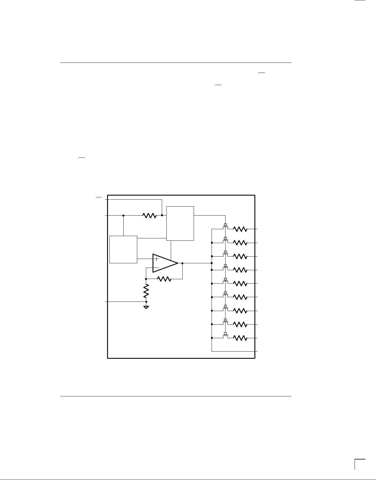
FUNCTIONAL DESCRIPTION
The DS2105 consists of a bandgap reference, buffer
amplifier, and nine termination resistors (Figure 1). The
bandgap reference circuit produces a precise 2.55V
level which is fed to a buffer amplifier. The buffer produces a 2.85V level and is capable of sourcing at least
24 mA into each of the termination resistors when the
signal line is low (active). When the driver for a given
signal line turns off, the terminator will pull the signal line
to 2.85V (quiescent state). To handle actively negated
SCSI signals, the buffer can sink 200 mA, and V
REF
will
move less than 60 mV . When all lines settle in the quiescent state, the regulator will consume about 5 mA.
When the DS2105 is put into power–down mode by
bringing PD low, the power–down circuitry will turn off
the transistors on each signal line. This will isolate the
DS2105 from the signal lines and effectively remove it
DS2105 BLOCK DIAGRAM Figure 1
PD
TERMPWR1
TERMPWR2
GND
BANDGAP
REFERENCE
50K ohm
from the circuit. The power–down pin (PD
nal 50KΩ pull–up resistor. To place the DS2105 into an
active state, the PD pin should be left open circuited.
T o ensure proper operation, both the TERMPWR1 and
TERMPWR2 pins must be connected to the SCSI bus
TERMPWR line and both the VREF1 and VREF2 pins
must be tied together externally . Each DS2105 requires
a 4.7 µF capacitor connected between the VREF pins
and ground. Figure 2 details a typical SCSI bus configuration. In an 8–bit wide SCSI bus arrangement (“A”
Cable), two DS2105’s would be needed at each end of
the SCSI cable in order to terminate the 18 active signal
lines. In a 16–bit wide SCSI bus arrangement (“P”
Cable), three DS2105’s would be needed at each end of
the SCSI cable in order to terminate the 27 active signal
lines.
POWER
DOWN
CIRCUITRY
110 ohms
R1
110 ohms
R2
110 ohms
R3
110 ohms
R4
110 ohms
R5
110 ohms
R6
110 ohms
110 ohms
110 ohms
) has an inter-
R7
R8
R9
022698 2/7
VREF1
VREF2
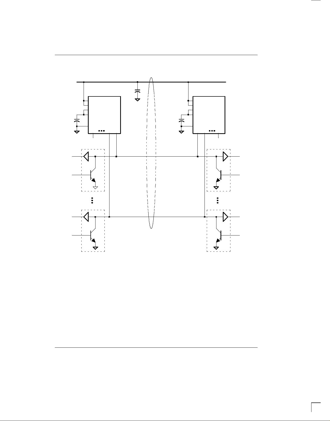
TYPICAL SCSI BUS CONFIGURATION Figure 2
Termination Power Line
DS2105
C1
DS2105
TERMPWR1
TERMPWR2
VREF1
+
VREF2
GND
R1 R2R9
R8
SCSI
BUS
TRANSCEIVER
+
C2
SCSI
CABLE
+
C1
SCSI
BUS
TRANSCEIVER
DS2105
TERMPWR1
TERMPWR2
VREF1
VREF2
GND
R1 R9
SCSI
BUS
TRANSCEIVER
SCSI
BUS
TRANSCEIVER
NOTES:
1. C1 = 4.7 µF tantalum
C2 = 2.2 µF tantalum or 4.7 µF aluminum
2. If the DS2105 is to be embedded into a peripheral that will act as a target on a SCSI bus, it is recommended that
TERMPWR be derived from the SCSI cable, not generated locally. In this configuration, if a power failure occurs
in the peripheral, it will not affect the bus.
3. A high frequency bypass capacitor (0.1 µF recommended) can be added in parallel to C1 for applications using
fast rise/fall time drivers.
022698 3/7
 Loading...