

Dallas Semiconductor DS2064S-200, DS2064-200 Datasheet
DS2064
DS2064
8K x 8 Static RAM
FEATURES
• Low power CMOS design
• Standby current
50 nA max at t
100 nA max at tA = 25°CVCC = 5.5V
1 µA max at t
• Full operation for V
= 25°CVCC = 3.0V
A
= 60°CVCC = 5.5V
A
= 4.5V to 5.5V
CC
• Data Retention Voltage = 5.5V to 2.0V
• Access time equals 200 ns at 5.0V
• Operating temperature range of –40°C to +85°C
• Full static operation
• TTL compatible inputs and outputs
• Available in 28–pin DIP and 28–pin SOIC packages
• Suitable for both battery operated and battery backup
applications
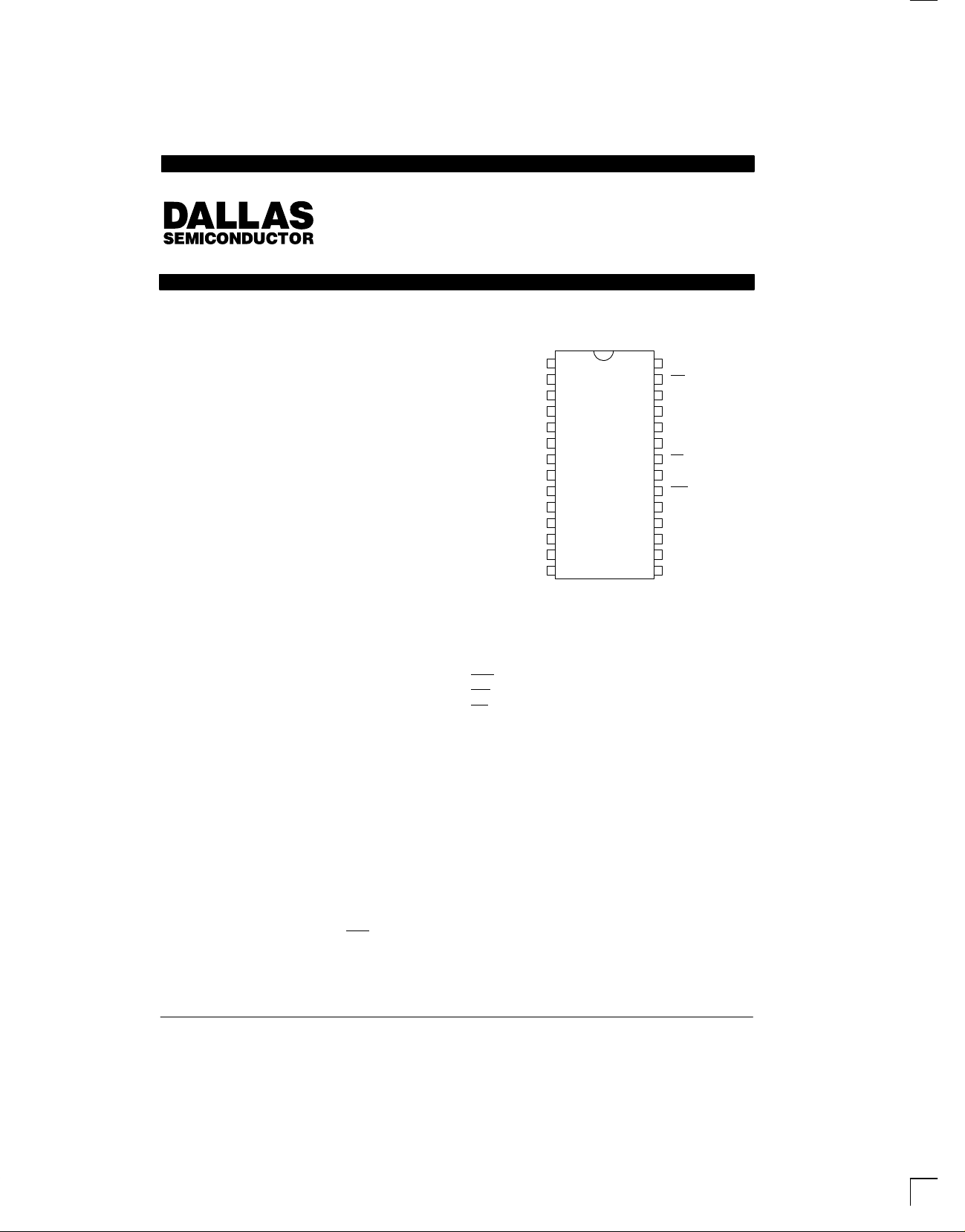
PIN ASSIGNMENT
1
NC
2
A12
3
A7
4
A6
5
A5
6
A4
7
A3
8
A2
9
A1
10
A0
11
DQ0
12
DQ1
13
DQ2
14
GND
DS2064–200 28–PIN DIP (600 MIL)
DS2064S–200 28–PIN SOIC (330 MIL)
28
27
26
25
24
23
22
21
20
19
18
17
16
15
PIN DESCRIPTION
A0–A12 – Address Inputs
DQ0–DQ7 – Data Input/Output
CE1, CE2 – Chip Enable Inputs
WE – Write Enable Input
OE
V
CC
GND – Ground
NC – No Connection
– Output Enable Input
– 5V Power Supply Input
V
CC
WE
CE2
A8
A9
A11
OE
A10
CE1
DQ7
DQ6
DQ5
DQ4
DQ3
DESCRIPTION
The DS2064 is a 65536–bit low power, fully static random access memory organized as 8192 words by eight
bits using CMOS technology. The device operates from
a single power supply with a voltage input between 4.5V
and 5.5V. The chip enable inputs (CE1 and CE2) are
used for device selection and can be used in order to
achieve the minimum standby current mode, which fa-
cilitates both battery operate and battery backup applications. The device provides fast access time of 200 ns
and is most suitable for low power applications where
battery operation or battery backup for nonvolatility are
required. The DS2064 is a JEDEC–standard 8K x 8
SRAM and is pin–compatible with ROM and EPROM of
similar density.
022598 1/9
DS2064
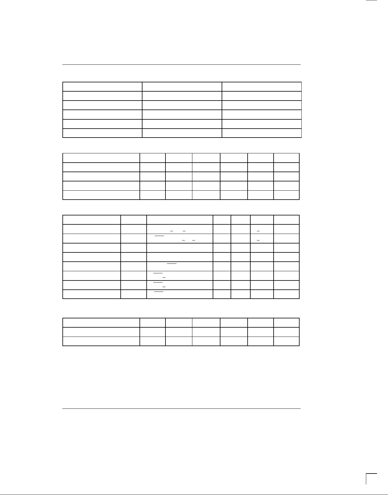
ABSOLUTE MAXIMUM RATINGS
SYMBOL PARAMETER RATING
V
CC
VIN, V
T
STG
T
OPR
T
SOLDER
I/O
Power Supply Voltage –0.3V to +7.0V
Input, Input/Output Voltage –0.3 to VCC + 0.3V
Storage Temperature –55°C to +125°C
Operating Temperature –40°C to +85°C
Soldering Temperature/Time 260 °C for 10 seconds
RECOMMENDED DC OPERATING CONDITIONS (tA = –40°C to +85°C)
PARAMETER SYMBOL MIN TYP MAX UNITS NOTES
Power Supply Voltage V
Input High Voltage V
Input Low Voltage V
Data Retention Voltage V
CC
IH
IL
DR
4.5 5.0 5.5 V
2.0 VCC + 0.3 V
–0.3 0.8 V
2.0 5.5 V
DC CHARACTERISTICS (tA = –40°C to +85°C; VCC=5V ± 10%)
PARAMETER SYMBOL CONDITIONS MIN TYP MAX UNITS
Input Leakage Current I
I/O Leakage Current I
Output High Current I
Output Low Current I
Standby Current I
Standby Current I
Standby Current I
Operating Current I
IL
LO
OH
OL
CCS1
CCS2
CCS2
CCO
0V < VIN < V
CE1=V
0V<VIO<V
IH,
CC
CC
+0.1 µA
+0.5 µA
VOH = 2.4V –1.0 mA
VOL = 0.4V 4.0 mA
CE1 = 2.0V 0.5 mA
CE1>VCC–0.5V tA=60°C 1 µA
CE1>VCC–0.5V tA=25°C 100 nA
CE1=0.8V, 200 ns cycle 70 mA
CAPACITANCE (tA = 25°C)
PARAMETER SYMBOL MIN TYP MAX UNITS NOTES
Input Capacitance C
Input/Output Capacitance C
022598 2/9
IN
I/O
5 10 pF
5 12 pF

DS2064
AC CHARACTERISTICS, READ CYCLE (tA = –40°C to +85°C; VCC=5V ± 10%)
PARAMETER SYMBOL MIN TYP MAX UNITS NOTES
Read Cycle Time t
Access Time t
OE to Output Valid t
CE to Output Valid t
CE or OE to Output Active t
Output to High–Z from
Deselection
Output Hold from Address
Change
RC
ACC
OE
CO
COE
t
OD
t
OH
200 ns
200 ns
100 ns
200 ns
5 ns
10 60 ns
5 ns
AC CHARACTERISTICS, WRITE CYCLE (tA = –40°C to +85°C; VCC=5V ± 10%)
PARAMETER SYMBOL MIN TYP MAX UNITS NOTES
Write Cycle Time t
Write Pulse Width t
Address Setup Time t
Write Recovery Time t
Output High–Z from WE t
Output Active from WE t
Data Setup Time t
Data Hold Time t
WC
WP
AW
WR
ODW
OEW
DS
DH
200 ns
150 ns
0 ns
10 ns
70 ns 7
5 ns 7
80 ns
0 ns
TIMING DIAGRAM: READ CYCLE
ADDRESSES
CE t
OE
D
OUT
SEE NOTE 1
t
RC
V
IH
V
IL
t
V
ACC
IH
CO
V
IL
V
IH
t
OE
V
IL
t
COE
t
COE
V
OH
V
OL
V
V
V
IH
V
IH
OUTPUT
DATA VALID
IH
IL
V
IH
V
IL
t
OH
t
OD
t
OD
V
OH
V
OL
022598 3/9
 Loading...