dallas semiconductor DS1867 service manual

DS1867
Dual Digital Potentiometer with EEPROM
www.dalsemi.com
FEATURES
§ Nonvolatile version of the popular DS1267
§ Low power consumption, quiet, pumpless
design
§ Operates from single 5V or ±5V supplies
§ Two digitally controlled, 256-position
potentiometers
§ Wiper position is maintained in the absence of
power
§ Serial port provides means for setting and
reading both potentiometers
§ Resistors can be connected in series to
provide increased total resistance
§ 16-pin SOIC and 20-pin TSSOP for surface
mount applications
§ Standard resistance values:
- DS1867-10 ~ 10 kΩ
- DS1867-50 ~ 50 kΩ
- DS1867-100 ~ 100 kΩ
§ Operating Temperature Range:
- Industrial: -40°C to +85°C
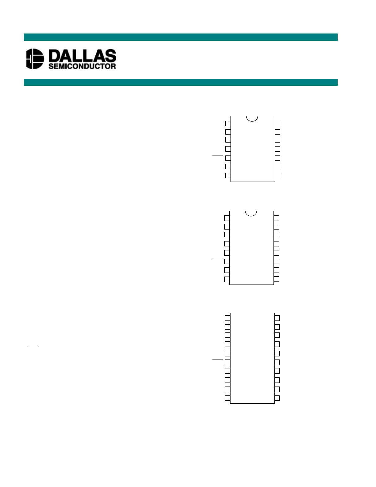
PIN ASSIGNMENT
V
H1 2 13 S
L1 3 12 WO
RST 5 10 LO
CLK 6 9 C
GND 7 8 DQ
14-Pin DIP (300-mil)
See Mech. Drawings Section
V
RST 6 11 LO
CLK 7 10 C
GND 8 9 DQ
1 14 V
B
W1 4 11 HO
1 16 V
B
NC 2 15 NC
H1 3 14 S
L1 4 13 WO
W1 5 12 HO
CC
OUT
OUT
CC
OUT
OUT
PIN DESCRIPTION
L0, L1 - Low End of Resistor
H0, H1 - High End of Resistor
W1, W2 - Wiper End of Resistor
V
B
S
OUT
RST
DQ - Serial Port Data Input
CLK - Serial Port Clock Input
C
OUT
VCC - +5-Volt Supply Input
GND - Ground
NC - No Internal Connection
DNC - Do Not Connect
- Substrate Bias
- Wiper for Stacked Configuration
- Serial Port Reset Input
- Cascade Serial Port Output
16-Pin SOIC (300-mil)
See Mech. Drawings Section
VB1 20 V
NC 2 19 DNC
H1 3 18 DNC
L1 4 17 S
W1 5 16 WO
RST 6 15 HO
CLK 7 14 LO
DNC 8 13 C
DNC 9 12 DNC
GND 10 11 DQ
20-Pin TSSOP (173-mil)
See Mech. Drawings Section
CC
OUT
OUT
1 of 14 102199

DS1867
DESCRIPTION
The DS1867 Dual Digital Potentiometer with EEPROM is the nonvolatile version of the popular DS1267
Dual Digital Potentiometer. The DS1867 consists of two digitally controlled potentiometers having 256position wiper settings. Wiper position is maintained in the absence of power through the use of
EEPROM memory cell arrays. Communication and control of the device are accomplished over a 3-wire
serial port which allows reads and writes of the wiper position. Both potentiometers can be stacked for
increased total resistance with the same resolution. For multiple-device, single-processor environments,
the DS1867 can be cascaded for control over a single 3-wire bus. The DS1867 is offered in three standard
resistance values.
OPERATION
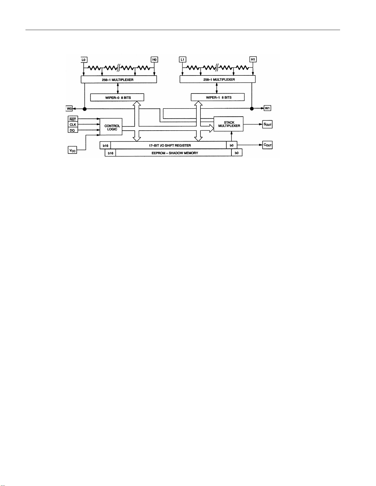
The DS1867 contains two 256-position potentiometers whose wiper positions are set by an 8-bit value.
These two 8-bit values are written to a 17-bit I/O shift register which is used to store wiper position and
the stack select bit when the device is powered. An additional memory area, the shadow memory, stores
the 17-bit I/O shift register during a power-down sequence which provides for wiper nonvolatility. A
block diagram of the DS1867 is presented in Figure 1.
Communication and control of the DS1867 is accomplished through a 3-wire serial port interface that
drives an internal control logic unit. The 3-wire serial interface consists of the three input signals: RST ,
CLK, and DQ.
The RST control signal is used to enable 3-wire serial port operation of the device. The RST signal is an
active high input and is required to begin any communication to the DS1867. The CLK signal input is
used to provide timing synchronization for data input and output. The DQ signal line is used to transmit
potentiometer wiper settings and the stack select bit configuration to the 17-bit I/O shift register of the
DS1867.
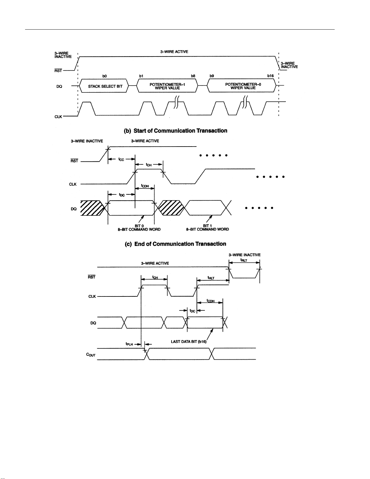
Figure 2(a) presents the 3-wire serial port protocol. As shown, the 3-wire port is inactive when the RST
signal input is low. Communication with the DS1867 requires the transition of the RST input from a low
state to a high state. Once the 3-wire port has been activated, data is latched into the part on the low to
high transition of the CLK signal input. Three-wire serial timing requirements are provided in the timing
diagrams of Figure 2(b) and (c).
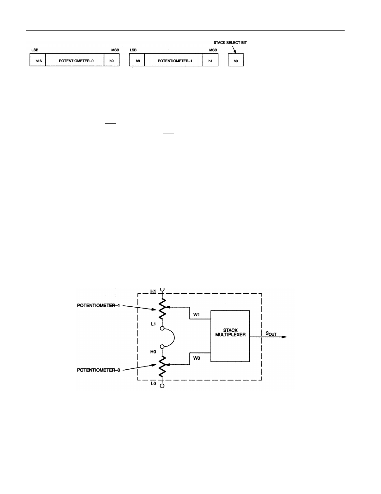
Data written to the DS1867 over the 3-wire serial interface is stored in the 17-bit I/O shift register (see
Figure 3). The 17-bit I/O shift register contains both 8-bit potentiometer wiper position values and the
stack select bit. The composition of the I/O shift register is presented in Figure 3. Bit 0 of the I/O shift
register contains the stack select bit. This bit will be discussed in the section entitled Stacked
Configuration. Bits 1 through 8 of the I/O shift register contain the potentiometer-1 wiper position value.
Bit 1 will contain the MSB of the wiper setting for potentiometer-1 and bit 8 the LSB for the wiper
setting. Bits 9 through 16 of the I/O shift register contain the value of the potentiometer-0 wiper position
with the MSB for the wiper position occupying bit 9 and the LSB bit 16.
2 of 14 102199

DS1867 BLOCK DIAGRAM Figure 1
DS1867
3 of 14 102199

TIMING DIAGFRAMS Figure 2
(a) 3-Wire Serial Interface General Overview
DS1867
4 of 14 102199

DS1867
I/O SHIFT REGISTER Figure 3
17-BIT I/O SHIFT REGISTER
Transmission of data always begins with the stack select bit followed by the potentiometer-1 wiper
position value and lastly the potentiometer-0 wiper position value (see Figure 2(a)).
When wiper position data is to be written to the DS1867, 17-bits (or some integer multiple) of data should
always be transmitted. Transactions which do not send a complete 17-bits (or multiple) will leave the
register incomplete and possibly an error in desired wiper position. After a communication transaction
has been completed the RST signal input should be taken to a low state to prevent any inadvertent
changes to the device shift register. Once RST has reached a low state, the contents of the I/O shift
register are loaded into the respective multiplexers for setting wiper position. A new wiper position will
only engage pending a RST transition to the low state. The wiper position for the high-end terminals H0
and H1 will have data values FF (hex), while the low-end terminals will have data values 00 (hex).
STACKED CONFIGURATION
The potentiometers of the DS1867 can be connected in series as shown in Figure 4. This is referred to as
the stacked configuration and allows the user to double the total end-to-end resistance of the part. The
resolution of the combined potentiometers will remain the same as a single potentiometer but with a total
of 512 wiper positions available. Device resolution is defined as R
R
is equal to the device resistance value. The wiper output for the combined stacked potentiometer will
TOT
be taken at the S
potentiometer-1 (W1). The potentiometer wiper selected at the S
pin, which is the multiplexed output of the wiper of potentiometer-0 (W0) or
out
out
the stack select bit (bit-0) of the 17-bit I/O shift register. If the stack select bit has value 0, the multiplexed
output, S
output, S
, will be that of the potentiometer-0 wiper. If the stack select bit has value 1, the multiplexed
out
, will be that of the potentiometer-1 wiper.
out
/256 (per potentiometer); where
TOT
output is governed by the setting of
STACKED CONFIGURATION Figure 4
CASCADE OPERATION
A feature of the DS1867 is the ability to control multiple devices from a single processor. Multiple
DS1867s can be linked or daisy-chained as shown in Figure 5. As a data bit is entered into the I/O shift
register of the DS1867 it will appear at the C
output after a maximum delay of 70 nanoseconds.
out
5 of 14 102199
 Loading...