

dallas semiconductor DS1855 service manual
r
y
查询DS1855供应商
www.maxim-ic.com
FEATURES
§ Two linear taper potentiometers
- DS1855-010 (one 10k, 100 position and
one 10k, 256 position)
- DS1855-020 (one 10k, 100 position and
one 20k, 256 position)
- DS1855-050 (one 10k, 100 position and
one 50k, 256 position)
- DS1855-100 (one 10k, 100 position and
one 100k, 256 position)
§ 256 bytes of EEPROM memory
§ Access to data and potentiometer control via
a 2-wire interface
§ External write-protect pin to protect data and
potentiometer settings
§ Data and potentiometer settings also can be
write-protected through software control
§ Nonvolatile wiper storage
§ Operates from 3V or 5V supplies
§ Packaging: 14-pin TSSOP, 16-ball STPBGA,
flip-chip package
§ Industrial operating temperature:
-40ºC to +85ºC
§ Programming temperature: 0ºC to +85ºC
DS1855
Dual Nonvolatile Digital Potentiomete
and Secure Memor
SDA 1 14 Vcc
SCL 2
A0
GND
3
A1 4 11 H1
A2 5
WP 6 9 W0
78
14-Pin TSSOP (173-mil)
Top View
A
B
C
D
1 2 3 4
16-Ball STPBGA (4mm x 4mm)
14-Pin Flip Chip (100-mil x 100-mil)
(Not Shown)
10
13
12
H0
W1
L1
L0
DESCRIPTION
The DS1855 dual nonvolatile (NV) digital potentiometer and secure memory consists of one 100-position
linear taper potentiometer, one 256-position linear taper potentiometer, 256 bytes of EEPROM memory,
and a 2-wire interface. The DS1855, which features a new software write protect, is an upgrade of the
DS1845. The DS1855 provides an ideal method for setting bias voltages and currents in control
applications using a minimum of circuitry. The EEPROM memory allows a user to store configuration or
calibration data for a specific system or device as well as provide control of the potentiometer wiper
settings. Any type of user information may reside in the first 248 bytes of this memory. The next two
addresses of EEPROM memory are for potentiometer settings and the remaining 6 bytes of memory are
reserved. These reserved and potentiometer registers should not be used for data storage. Access to this
EEPROM is via an industry-standard 2-wire bus. The interface I/O pins consist of SDA and SCL. The
wiper position of the DS1855, as well as EEPROM data, can be write-protected through hardware using
the write-protect input pin (WP) or software using the 2-wire interface.
1 of 20 100101

PIN DESCRIPTIONS
Name TSSOP BGA Description
V
CC
GND 7 D1 Ground Terminal.
SDA 1 B2 2-Wire serial data interface. The serial data pin is for serial data
SCL 2 A2 2-Wire Serial Clock Input. The serial clock input is used to
WP 6 C1 Write Protect Input. If set to logic 0, the data in memory and the
A0 3 A1 Address Input. Pins A0, A1, and A2 are used to specify the
A1 4 B1 Address Input.
A2 5 C2 Address Input.
H0 13 A4 High terminal of Potentiometer 0. For both potentiometers, it is
H1 11 B3 High terminal of Potentiometer 1.
L0 8 D3 Low terminal of Potentiometer 0. For both potentiometers, it is
L1 10 C4 Low terminal of Potentiometer 1.
W0 9 D4 Wiper terminal of Pot 0. The wiper position of Potentiometer 0
W1 12 B4 Wiper terminal of Pot 1. The wiper position of Potentiometer 1
NC C3 No Connect.
NC D2 No Connect.
14 A3 Power Supply Terminal. The DS1855 will support supply
voltages ranging from +2.7V to +5.5V.
transfer to and from the DS1855. The pin is open drain and may
be wire-ORed with other open drain or open collector interfaces.
clock data into the DS1855 on rising edges and clock data out on
falling edges.
potentiometer wiper setting may be changed. If set to logic 1, both
the memory and the potentiometer wiper settings will be write
protected. The WP pin is pulled high internally.
address of each DS1855 when used in a multi-dropped
configuration. Up to eight DS1855s may be addressed on a single
2-wire bus.
not required that the high terminal be connected to a potential
greater than the low terminal. Voltage applied to the high terminal
of each potentiometer cannot exceed VCC or go below ground.
not required that the low terminal be connected to a potential less
than the high terminal. Voltage applied to the low terminal of each
potentiometer cannot exceed VCC or go below ground.
is determined by the byte at EEPROM memory location F9h.
Voltage applied to the wiper terminal of each potentiometer cannot
exceed the power supply voltage, V
, or go below ground.
CC
is determined by the byte at EEPROM memory location F8h.
DS1855
2 of 20
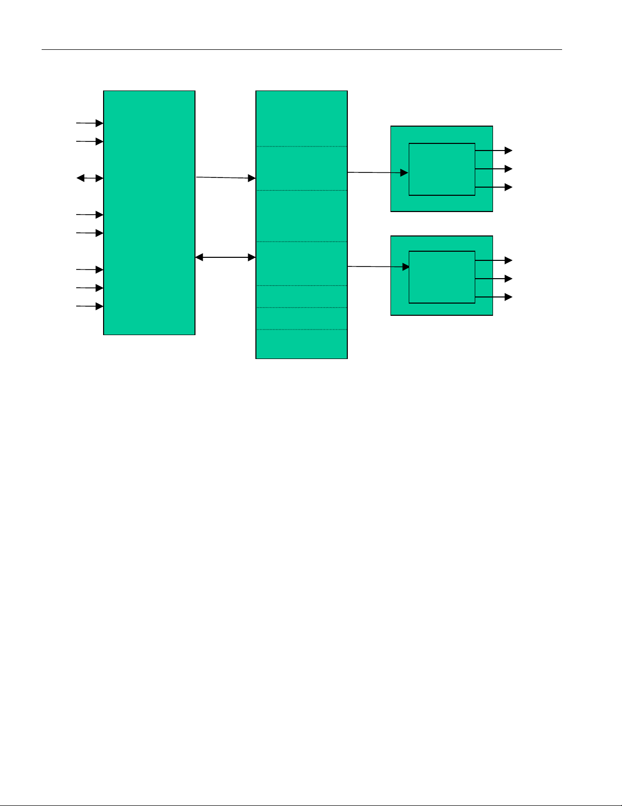
DS1855 BLOCK DIAGRAM Figure 1
DS1855
V
CC
GND
SDA
SCL
WP
A0
A1
A2
2-WIRE
INTERFACE
CONTROL
DATA
248 BYTES
EEPROM
MEMORY
1 BYTE WIPER
SETTING
POT 0
1 BYTE WIPER
SETTING
POT 1
CONFIGURATION
BYTE
LOCK BYTE
LOCK BYTE
RESERVED
POTENTIOMETER 0
100-
Position
Pot
POTENTIOMETER 1
256-
Position
Pot
H0
W0
L0
H1
W1
L1
Up to eight DS1855s can be installed on a single 2-wire bus. Access to an individual device is achieved
by using a device address that is determined by the logic levels of address pins A0 through A2.
Additionally, the DS1855 will operate from 3V or 5V supplies. Three package options are available: 14pin TSSOP, 16-ball STPBGA, and flip-chip package.
3 of 20

DS1855
MEMORY ORGANIZATION
The DS1855’s serial EEPROM is internally organized with 256 words of 1 byte each. Each word requires
an 8-bit address for random word addressing. The byte at address F9h determines the wiper setting for
potentiometer 0, which contains 100 positions. Writing values above 63h to this address sets the wiper to
its uppermost position, but the MSB is ignored. The byte at address F8h determines the wiper setting for
potentiometer 1, which contains 256 positions (00h to FFh). Address locations FAh though FFh are
reserved and should not be written.
MEMORY
LOCATION
NAME OF
MEMORY
FUNCTION OF MEMORY LOCATION
LOCATION
00h – F7h User Memory General-purpose user memory.
F8h Potentiometer 1 Setting Writing to this byte controls the setting of potentiometer 1, a 256-
position pot. Valid settings are 00h to FFh.
F9h Potentiometer 0 Setting Writing to this byte controls the setting of potentiometer 0, a 100-
position pot. Valid settings are 00h to 63h. MSB is ignored.
FAh Software Lock
Configuration Byte
The three lower bits in this byte can be used to set write-protection
to the 256-byte memory block.
B2 B1 B0
B2: Writing this bit to a 1 protects the upper page of memory. If
this bit is set, memory locations F8h to FFh are configured for
write-protection.
B1: Writing this bit to a 1 protects the upper block of memory. If
this bit is set, memory locations 80h to F7h are configured for
write-protection. The upper page must be unlocked in order to
modify the locking of this portion of memory.
B0: Writing this bit to a 1 protects the lower block of memory. If
this bit is set, memory locations 00h to 7Fh are configured for
write-protection. The upper page must be unlocked in order to
modify the locking of this portion of memory.
4 of 20

DS1855
FBh – FCh Lock Bytes Writing to these two bytes allows the user to lock or unlock the
memory described in byte FAh.
LOCK: If memory location FBh is written to 56h and memory
location FCh is written to 25h, the device will enter lock mode.
Write protection will become active in the memory locations that
are specified in FAh.
UNLOCK: If memory location FBh is written to 67h and memory
location FCh is written to 36h, the device will be unlocked. Once
unlocked, the user can change the setting of memory location FAh
to affect the EEPROM write-protection.
The locking can be updated at any time as long as the upper
page is unlocked.
FD – FFh Reserved Reserved
5 of 20

DS1855
2-WIRE OPERATION
Clock and Data Transitions
The SDA pin is normally pulled high with an external resistor or device. Data on the SDA pin may only
change during SCL low time periods. Data changes during SCL high periods will indicate a START or
STOP conditions depending on the conditions discussed below. Refer to the timing diagram in Figure 2
for further details.
START Condition
A high-to-low transition of SDA with SCL high is a START condition that must precede any other
command. Refer to the timing diagram in Figure 2 for further details.
STOP Condition
A low-to-high transition of SDA with SCL high is a STOP condition. After a read sequence, the stop
command places the DS1855 into a low-power mode. Refer to the timing diagram in Figure 2 for further
details.
Acknowledge
All address and data bytes are transmitted via a serial protocol. The DS1855 pulls the SDA line low
during the ninth clock pulse to acknowledge that it has received each word.
Standby Mode
The DS1855 features a low-power mode that is automatically enabled after power-on, after a STOP
command, and after the completion of all internal operations.
2-Wire Interface Reset
After any interruption in protocol, power loss, or system reset, the following steps reset the DS1855:
1. Clock up to nine cycles.
2. Look for SDA high in each cycle while SCL is high.
3. Create a START condition while SDA is high.
Device Addressing
The DS1855 must receive an 8-bit device address word following a START condition to enable a specific
device for a read or write operation. The address word is clocked into the DS1855 MSB to LSB. The
address word consists of Ah (1010) followed by A2, A1, and A0 then the read/write (R/W) bit. If the
R/W bit is high, a read operation is initiated. If the R/W is low, a write operation is initiated. For a device
to become active, the values of A2, A1, and A0 must be the same as the hard-wired address pins on the
DS1855. Upon a match of written and hard-wired addresses, the DS1855 will output a zero for one clock
cycle as an acknowledge. If the address does not match, the DS1855 returns to a low-power mode.
Write Operations
After receiving a matching address byte with the R/W bit set low, the device goes into the write mode of
operation. The master must transmit an 8-bit EEPROM memory address to the device to define the
address where the data is to be written. After the reception of this byte, the DS1855 will transmit a zero
for one clock cycle to acknowledge the receipt of the address. The master must then transmit an 8-bit data
word to be written into this address. The DS1855 will again transmit a zero for one clock cycle to
acknowledge the receipt of the data. At this point, the master must terminate the write operation with a
STOP condition. The DS1855 then enters an internally timed write process T
to the EEPROM memory.
w
All inputs are disabled during this byte write cycle.
6 of 20
 Loading...