Dallas Semiconductor DS1807S-T-R, DS1807S, DS1807E-T-R, DS1807E, DS1807 Datasheet

1 of 13 110499
FEATURES
§ Operates from 3V or 5V Power Supplies
§ Ultra-low power consumption
§ Two digitally controlled, 65-position
potentiometers
§ Logarithmic resistor characteristics (1 dB per
step)
§ Zero-crossing detection eliminates noise
caused by discrete wiper changes
§ Addressable using 3-Chip Select Inputs
§ Serial/Synchronous Bus Inputs
§ Operating Temperature Range:
- Industrial: -40°C to +85°C
§ Standard Resistance Value: 45 kΩ
PIN ASSIGNMENT
PIN DESCIPTION
L0, L1 - Low End of Resistor
H0, H1 - High End of Resistor
W0,W1 - Wiper Terminal of Resistor
VCC - 3V/5V Power Supply Input
A0..A2 - Chip Select Inputs
SDA - Serial Data I/O
SCL - Serial Clock Input
GND - Ground
AGND - Analog Ground
NC - No connection
DESCRIPTION
The DS1807 Addressable Dual Audio Taper Potentiometer is a dual audio taper potentiometer having a
logarithmic resistive characteristic. Each potentiometer has a total of 65 wiper positions including the
mute position. Adjacent wiper positions are separated by 1 dB giving a total attenuation range of 64 dB.
When the wipers are in the mute position, attenuation in excess of 90 dB is achieved. The DS1807 also
provides a zero-crossing detection capability. This capability eliminates noise caused by discrete wiper
position changes. The DS1807 is controlled via a two-input, serial synchronous interface that provides the
capability of addressing up to eight different DS1807s. Addressability is obtained via communication
protocol and three (3) address select inputs A0, A1, and A2. Communication protocol allows for the exact
positioning of the DS1807 wiper’s position. Additionally, communication protocol allows for
independent or simultaneous setting of the two potentiometers' wipers. Wiper positions can also be read
via the 2-wire serial interface.
DS1807
Addressable Dual Audio Taper Potentiometer
www.dalsemi.com
GND 1 14 V
CC
A2 2 13 SCL
A1 3 12 SDA
A0 4 11 AGND
W0 5 10 H1
L0 6 9 L1
H0 7 8 W1
DS1807 14-Pin DIP (300-mil)
DS1807E 14-Pin TSSOP (173-mil)
GND 1 16 V
CC
A2 2 15 NC
A1 3 14 SCL
NC 4 13 SDA
A0 5 12 AGND
W0 6 11 H1
L0 7 10 L1
H0 8 9 W1
DS1807S 16-Pin SOIC (300-mil)
See mech. Drawings Section

DS1807
2 of 13 110499
The DS1807 is available in 14-pin DIP, SOIC, and TSSOP packages. The DS1807 is offered in industrial
temperature grades. The standard resistance of the DS1807 is 45 kΩ.
DEVICE OPERATION
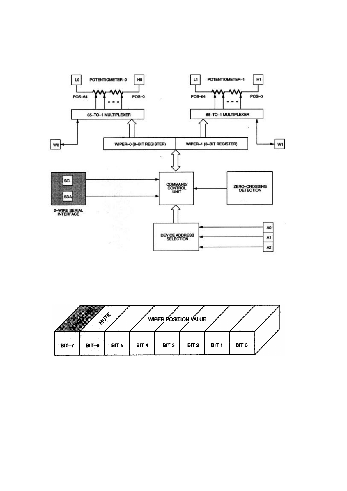
The DS1807 is an addressable, digitally controlled device that has two 65-position potentiometers. The
DS1807 potentiometers are logarithmic tapers providing a resolution or step size of 1 dB per step from
positions 0 through 63. The 64th position is the mute position and provides attenuation in excess of 90 dB.
Moving the potentiometer’s wiper from position 63 (or 63 dB of attenuation) to position 64 will provide a
step size in excess of 30 dB. A functional block diagram of the part is shown in Figure 1.
As stated, each potentiometer is composed of a 65 position resistor array. Two 8-bit registers, each
assigned to a respective potentiometer, are used to set wiper position on the resistor array. The wiper
terminal is multiplexed to one of 65 positions on the resistor array based on its corresponding 8-bit
register value.
Because the DS1807 has 65 positions, only seven bits of data are needed to set a wiper’s position. Bits 0
through 5 of the register are used to set the position on the resistor array. Bit 6 is used to set the wiper
position to the mute position and bit 7 is a don’t care. If the value of bit 6 is set equal to 1, regardless of
all other bit values, the wiper position of the respective potentiometer will be set to the mute position. An
example diagram of the wiper register and associated bit function is provided in Figure 2.
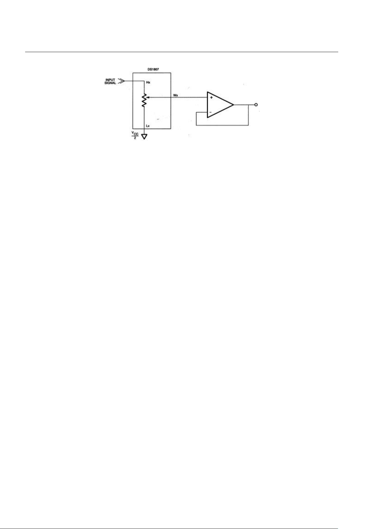
The DS1807 is designed to operate as an attenuator. ( see Figure 3) As such, wiper position values are set
with respect to the amount of attenuation desired. For example, if the user wishes to attenuate an
incoming signal by 6 dB, the wiper position register value(s) should be set to binary (0000 0110).
The H0 and H1 terminals of the DS1807 have wiper position values (binary) 0000 0000. These terminals
provide 0 dB of attenuation for the input signal. The L0 and L1 terminals provide the greatest attenuation
of the input signal. They represent the mute positions for the DS1807 and have wiper position values
(binary) 0100 0000 or greater.
On power-up, the serial port is stable and active within 10 microseconds. Additionally, DS1807 wiper
positions will be set to position 63 or (binary) 0011 1111, one position above mute. The user may then set
the wiper register to a desired value.
Communication with the DS1807 takes place over the 2-wire serial interface consisting of the bidirectional data terminal, SDA, and the serial clock input, SCL. The 2-wire serial interface and chip
select inputs A0, A1, and A2 allow operation of up to eight devices in a bus topology; with A0, A1, and
A2 being the physical address of the device. Complete details of the 2-Wire interface are discussed in the
section entitled “2-Wire Serial Data Bus.”

DS1807
3 of 13 110499
DS1807 BLOCK DIAGRAM Figure 1
WIPER REGISTER CONFIGURATION Figure 2

DS1807
4 of 13 110499
DS1807 ATTENUATOR CONFIGURATION Figure 3
ZERO-CROSSING DETECTION
The DS1807 provides many features for digitally controlled audio applications. Zero-crossing detection is
useful in eliminating “zipper noise,” which is commonly associated with digital potentiometers. Zipper
noise (because it sounds like a zipper) is caused by discrete wiper position changes on the resistor array.
These changes cause discontinuities in the audio output signal which are manifested as audible pops
heard at the output of the audio chain. If subsequent amplification follows the digital potentiometer, this
audible noise can be quite disturbing. The DS1807 minimizes zipper noise by allowing wiper position
changes only during zero-crossings of the input signal.
The zero-crossing detection feature can be enabled or disabled via software. The complete software
command for enabling or disabling zero-crossing is discussed in the section, “2-wire serial data bus.”
When enabled, the zero-crossing detection feature allows independent wiper changes within a 50
millisecond time window when the Hx and Lx (where x = 0 or 1) terminals have equal potentials. The 50
millisecond time window begins once the DS1807 has responded with an ACKNOWLEDGE after a
“write potentiometer “ command. The STOP condition is discussed in the following section.
If at 50 milliseconds the DS1807 has not detected a zero-crossing (Hx - Lx = 0), the wiper position of the
potentiometer(s) will change regardless of the state of the input signal.
When the zero-crossing detection feature is not activated, the DS1807 will allow movement to the new
wiper position as soon as the ACKNOWLEDGE condition has been issued by the master controlling
device.
The DS1807 is designed to provide the zero-crossing detection feature when initially powered. If this
feature is not to be used, it must be deactivated once the device has reached a fully powered condition.
2-WIRE SERIAL DATA BUS
The DS1807 supports a bi-directional 2-wire bus and data transmission protocol. A device that sends data
on the bus is defined as a transmitter, and a device receiving data as a receiver. The device that controls
the message is called a “master.” The devices that are controlled by the master are “slaves.” The bus must
be controlled by a master device which generates the serial clock (SCL), controls the bus access, and
generates the START and STOP conditions. The DS1807 operates as a slave on the 2-wire bus.
Connections to the bus are made via the open-drain I/O line, SDA, and the serial clock line, SCL.
The following bus protocol has been defined (See Figure 4).
§ Data transfer may be initiated only when the bus is not busy.
§ During data transfer, the data line must remain stable whenever the clock line is HIGH. Changes in
the data line while the clock line is high will be interpreted as control signals.
 Loading...