Dallas Semiconductor DS1801S-T-R, DS1801S, DS1801E-014-T-R, DS1801E-014, DS1801 Datasheet

1 of 10 030300
FEATURES
Ultra-low power consumption
Operates from 3V or 5V supplies
Two digitally controlled, 65-position
potentiometers including mute
Logarithmic resistive characteristics (1 dB
per step)
Zero-crossing detection eliminates noise
caused by wiper movement
Serial port provides means for setting and
reading both potentiometers wipers
14-pin PDIP, 16-pin SOIC, and 14-pin
TSSOP packages
Operating Temperature Range:
- Industrial: -40°C to +85°C
Software mute
Resistance available: 45 kΩ
PIN DESCRIPTION
L0, L1 - Low End of Resistor
H0, H1 - High End of Resistor
W0,W1 - Wiper End of Resistor
VCC - 3V or 5V Power Supply Input
RST - Serial Port Reset Input
D - Serial Port Data Input
CLK - Serial Port Clock Input
GND - Digital Ground
AGND - Analog Ground
ZCEN - Zero-Crossing Detect Input
C
OUT
- Cascade Output
NC - No Connect
PIN ASSIGNMENT
DESCRIPTION
The DS1801 is a dual audio taper potentiometer having logarithmic resistive characteristics over the
device range. Each potentiometer provides 65 wiper positions with a 1 dB increment per step and devic e
mute. The 3-wire serial interface, using a CPU, provides the user the ability of reading or writing exact
wiper positions of the two potentiometers. Additionally, the part contains a zero-crossing detection
feature that minimizes noise resulting from wiper transitions. Packages for the part include a 14-pin
PDIP, 16-pin SOIC, and 14-pin TSSOP.
DS1801
Dual Audio Taper Potentiomete
r
www.dalsemi.com
GND 1 14 VCC
COUT 2 13 CLK
RST 3 12 D
ZCEN 4 11 AGND
W0 5 10 H1
L0 6 9 L1
H0 7 8 W1
DS1801 14-Pin PDIP (300-mil)
DS1801 14-Pin TSSOP (173-mil)
GND 1 16 VCC
COUT 2 15 CLK
RST 3 14 D
ZCEN 4 13 NC
NC 5 12 AGND
W0 6 11 H1
L0 7 10 L1
H0 8 9 W1
DS1801S 16-PIN SOIC (300-mil)
See Mech. Drawings Section

DS1801
2 of 10
OPERATION
The DS1801 provides two 65-position potentiometers per package, each having a logarithmic resistive
characteristic as shown in Table 1. The DS1801 is controlled by a 3-wire serial interface. The 3-wire
serial interface is designed for CP U-controlled applications and allows the potentiometer’s exact wiper
position to be read or written. The DS1801 design supports daisy-chaining for multi-device
environments.
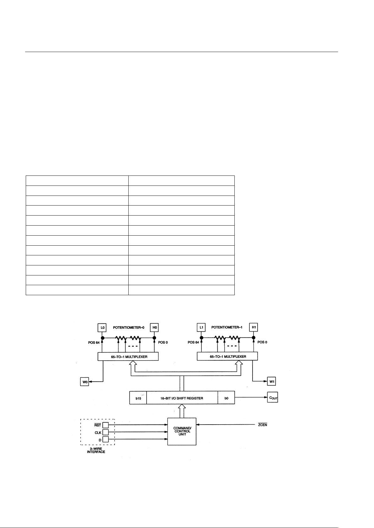
Figure 1 presents a block diagram of the DS1801. As shown, the inputs from the 3-wir e serial interface
drive a command/control unit. The command/control unit interprets these inputs for control of the two
potentiometers.
On power-up, the serial port is stable and active within 10 microseconds. The wiper position on power-up
will be at position 63, the low end of the potentiometer. Position 64 is the mute level.
RESISTANCE CHARACTERISTICS Table 1
POSITION OUTPUT LEVEL (dB)
00
1-1
2-2
3-3
4-4
5-5
63 -63
64(mute) <-90
DS1801 BLOCK DIAGRAM Figure 1

DS1801
3 of 10
3-WIRE SERIAL INTERFACE CONTROL
Communication and control of the DS1801 is accomplished through a 3-wire serial port interface that
drives an internal control logic unit. The 3-wire serial interface is designed for microprocessor or
microcontroller applications. The interface consists of three input signals which include RST , CLK and
D.
The
RST control signal is used to enable 3-wire serial port write operations. The CLK terminal is a clock
signal input that provides synchronization for data I/O while the D signal input serves to transfer
potentiometer wiper position settings to the device.
As shown in Figure 3, a 3-wire serial port operation begins with a transition of the
RST signal input to a
high state. Once the 3-wire port has been activated, data is clocked into the part on the low to high
transition of the CLK signal input. Data input via the D line is transferred in the order of the desired
potentiometer-0 value followed by the potentiometer-1 value.
The DS1801 contains two 65-position potentiometers whose wiper positions are set by an 8-bit value.
These two 8-bit values are written to the 16-bit I/O shift register which is used to store wiper position
during powered conditions. Because the potentiometer has 65-positions, only 7 bits of data are needed to
set wiper position. A detailed diagram of the 16-bit I/O shift register is shown in Figure 2. Bits 0 through
7 are reserved for the potentiometer-0 control while bits 8 through 15 are reserved for control of
potentiometer-1.
Bits 0 through 5 are used for actual wiper positioning of potentiometer-0. Bit 6 is used to mute
potentiometer-0. If this bit has value 1, the potentiometer-0 wiper will be connected to the low end of the
resistive array the mute position. The value of bit 7 is a “don’t care” and will not affect operation of the
DS1801 or potentiometer-0.
Bits 8 through 13 are used for wiper positioning of potentiometer-1. Bit 14 is used for muting of the
potentiometer-1 wiper output. Bit 15, like bit 7, is a “don’t care” and will not affect operation of the
DS1801.
Data for the DS1801 is transmitted LSB first starting with bit 0. A complete transmission of 16 bits of
data is required to insure proper setting of each potentiometer’s wiper. An incomplete transmission may
result in undesired wiper settings.
Once the complete 16 bits of information has been transmitted and the
RST signal input transitions to a
low state, the new wiper positions are loaded into the part.
16-BIT I/O SHIFT REGISTER Figure 2
 Loading...