dallas semiconductor DS1780 service manual

r
(
)
/
查询DS1780供应商
www.dalsemi.com
DS1780
CPU Peripheral Monito
FEATURES
Direct-to-digital temperature sensor requires
no external components or user calibration
Two fan speed sensors
Monitors 6 power supply voltages
8-bit DAC for fan speed control
Intrusion detect for security (detects when
chassis lid has been removed, even if power is
off)
Remote system reset
System interrupt availability on all monitored
functions (temperature, voltages, fan speed,
chassis intrusion)
2-wire interface with 2-bit addressability
Integrated NAND TREE for board level
testability
Wide power supply range (2.8V ≤ VDD ≤
5.75V)
High integration in a small 24-pin 173-mil
TSSOP
Applications include monitoring of personal
computers or any microprocessor-based
system
PIN ASSIGNMENT
A0/NT
OUT
A1
SDA
SCL
FAN1
FAN2
CHS
GNDD
V
DD
INT
NT
V
OUT
IN
RST
24-Pin TSSOP
1
2
3
4
5
6
7
8
9
10
11
12
DS1780E
24
23
22
21
20
19
18
17
16
15
14
13
173-mil
VID0
VID2
VID3
VID4
+V
CCP1
+2.5 V
IN
+3.3 V
IN
+5 V
IN
+12 V
IN
+2.5 VS/+V
GNDA
CCP2
PIN DESCRIPTION
A0/NT
OUT
TREE Output
A1 - Address Input
SDA - 2-Wire Serial Data
SCL - 2-Wire Serial Clock
FANx - Tachometer Inputs
CHS - Chassis Intrusion Detector
GNDD - Digital Ground
V
DD
INT - Hardware Interrupt output
V
/NT
OUT
IN
RST - Remote System Reset
GNDA - Analog Ground
+xxV
IN
+2.5V
/+V
S
CCP2
VIDx - Processor Voltage Supply
- Address Input / NAND
Input/Output
Input
- Power Supply Voltage (2.8V
to 5.75V)
- DAC output / NAND TREE
Input
- Positive Voltage Inputs
- Positive/negative Voltage
Input
Readout Inputs
1 of 28 111999

DS1780
DESCRIPTION
The DS1780 is a highly integrated system instrumentation monitor ideal for use in personal computers, or
any microprocessor-based system. It monitors ambient temperature, six power supply voltages, and the
speed of two fans. Fan speed can also be controlled with the use of an internal 8-bit DAC. All
measurements are internally converted to a digital format for easy processing by the CPU.
The DS1780 can be reset to its default power-up state via a remote reset function with internal debounce
and delay. It features an interrupt that can be programmed to become active should any of the functions
the DS1780 is monitoring fall out of spec.
For board-level testability, an internal NAND TREE function simplifies the system design. A chassis
intrusion input is featured to enhance system security.
Programming and data readout are accessed via a simple 2-wire interface with 2-bit addressability. The
DS1780 power supply range of 2.8V to 5.75V allows for monitoring of parameters for 3V or 5V systems.
The DS1780 is assembled in a compact 173-mil TSSOP package.
Detailed Pin Description Table 1
PIN SIGNAL DIRECTION DESCRIPTION
1A0/NT
2 A1 Digital Input The highest order programmable bit of the 2-wire bus address.
3 SDA Digital I/O 2-wire bus bi-directional data. Open-drain output.
4 SCL Digital Input 2-wire bus synchronous clock.
5 FAN1 Digital Input 0 to VDD amplitude fan tachometer input.
6 FAN2 Digital Input 0 to VDD amplitude fan tachometer input.
7 CHS Digital I/O
8 GNDD GROUND Internally connected to all digital circuitry.
9VDDPOWER
10
11 V
12
13 GNDA GROUND
14 +2.5VS/+V
15-19 +xxV
20-24 VIDx Digital Inputs
OUT
INT
/NT
RST
OUT
IN
CCP2
IN
Digital I/O
Digital Output
Digital Input/
Analog Output
Digital I/O
Analog Input
Analog Inputs A/D inputs for 5 positive voltages.
The lowest order programmable bit of the 2-wire bus address. This pin
functions as an output when doing a NAND TREE test.
An active high input from an external circuit, which latches a Chassis
Intrusion event. This line can go high without any clamping action regardless
of the powered state of the DS1780. The DS1780 provides an internal open
drain on this line, controlled by Bit 6 of Configuration Register, to provide a
minimum 20 ms reset of this signal.
+3.3V or +5V V
(Electrolytic or Tantalum) and 0.1 µF (ceramic) bypass capacitors.
Active-low Programmable interrupt output. The output is enabled when Bit 1
of the Configuration Register is set to 1. The default state is disabled.
An active-high input that enables NAND Tree board-level connectivity
testing. Refer to “NAND Tree Testing” Section. Used as DAC output when
NAND Tree is not selected.
Master Reset, 5 mA open drain driver, active low output with at least a 20 ms
minimum pulse width. Available when enabled via Bit 4 in Configuration
Register. This is a bi-directional I/O pin. It acts as power on RESET input.
Internally connected to all analog circuitry. The ground reference for all
analog inputs.
Analog input for monitoring -12V or +V
on this pin from 0V to 3.6V. An external resistor ladder is required for
monitoring a -12V supply (see Figure 1).
Voltage supply readouts from the processor. These values are read in the VID
and VID4 Status Registers.
power. Bypass with the parallel combination of 10 µF
DD
. DS1780 will measure voltages
CCP2
2 of 28

DS1780
OVERVIEW
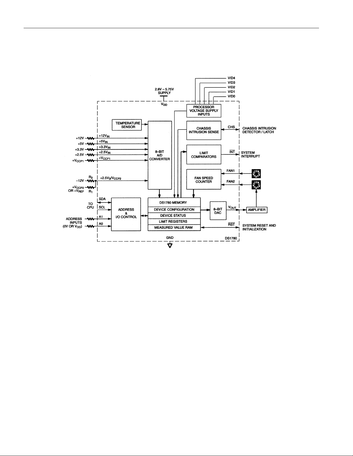
A block diagram of the DS1780 is shown in Figure 1.
The DS1780 provides six analog inputs, an analog output, five digital inputs, two fan speed inputs, a
temperature sensor, and interrupt registers on a single chip, which communicates on a 2-wire serial bus.
The DS1780 performs power supply, temperature, and fan monitoring for personal computers.
The analog voltages are divided internally by the DS1780. The inputs are then converted to 8-bit digital
words. The analog inputs are intended to be connected to the several power supplies present in a typical
computer. Temperature can be converted to a 9-bit two’s-complement digital word with a 0.5°C LSb.
The analog output is approximately a 0-1.25V output from an 8-bit D/A converter, which is used to
control fan speeds.
Fan inputs measure the period of tachometer pulses from the fans, providing a higher count for lower fan
speeds. The fan inputs are digital inputs with an acceptable range of 0 to VDD volts and a transition level
of approximately 1.4 volts. Full-scale fan counts are 255 (8-bit counter) and this represents a stopped or
very slow fan. Nominal speeds, based on a count of 153, are programmable from 1100 to 8800 RPM on
FAN1 and FAN2. Signal conditioning circuitry is included to accommodate slow rise and fall times.
The DS1780 provides a number of internal registers, as detailed in Table 1. These include:
Configuration Register: Provides control and configuration, as well as initialization.
Interrupt ( INT ) Status Registers: Two registers to provide status of each interrupt limit or interrupt
event.
Interrupt ( INT ) Mask Registers: Allows masking of individual Interrupt sources, as well as separate
masking for the hardware interrupt output.
Temperature Configuration Register: The lower 2 bits of this register configure the type of
temperature interrupt mode to be used. Bit 7 reflects the lowest bit of the temperature reading.
VID Register, VID4 Register: Bits 0-3 of the VID register reflect the status of the VID0-VID3 pins, bit
0 of the VID4 register reflect the status of VID4 pin. These are simply input pins - not processed in any
way. In a multiprocessor system, these signals will be multiplexed externally from the various processor
sources, with the source being controlled by software.
Value RAM: The monitoring results and limits for temperature, voltages, and fan counts are all
contained in the Value RAM.
When the DS1780 is started, it cycles through each measurement in sequence, and it continuously loops
through the sequence approximately once every second. Each measured value is compared to values
stored in limit registers. When the measured value violates the programmed limit the DS1780 will set a
corresponding System Management Interrupt (SMI) in the Interrupt Status Registers. One hardware
interrupt line, INT , is available to generate an SMI. INT is fully programmable with masking of each
Interrupt source, and masking of the output. In addition, the configuration register has control bits to
enable or disable the hardware Interrupts.
3 of 28

DS1780
A CHS (Chassis Intrusion) digital input is provided. The Chassis Intrusion input is designed to accept an
active high signal from an external circuit that latches when the case is removed from the computer; this
pin is a dual purpose pin which will be driven low by the DS1780 to reset the external circuit.
DS1780 FUNCTIONAL BLOCK DIAGRAM Figure 1
Note: R1 and R2 on the -12V resistance ladder should be ratioed such that approximately +2.5V appears
at the input pin (i.e., R1=4kΩ, R2=23.2 kΩ). If a second processor voltage needs to be monitored (V
leave R2 empty, and make R1 500Ω, with V
appearing here.
CCP2
CCP2
2-WIRE SERIAL DATA BUS
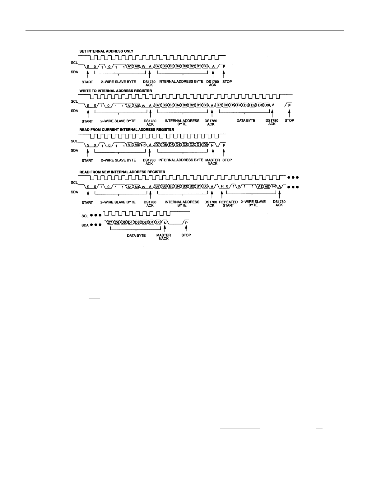
When using the 2-wire bus, a write will always consist of the DS1780 2-wire slave address, followed by
the Internal Address Register byte, then the data byte. The Internal Address Register addresses are listed
below in Table 2. There are two cases for a read:
1. If the Internal Address Register is known to be at the desired Address, simply read the DS1780 with
the 2-wire slave address, followed by the data byte read from the DS1780.
2. If the Internal Address Register value is unknown, write to the DS1780 with the 2-wire slave address,
followed by the Internal Address Register byte. Then restart the Serial Communication with a Read
consisting of the 2-wire slave address, followed by the data byte read from the DS1780.
The default power-on 2-wire slave address for the DS1780 is 01011(A1)(A0) binary, where A0-A1
reflects the state of the pins defined by the same names. The address can be changed by writing any
desired value to the 2-wire Serial Address Register (excluding the 2 LSBs). This communication protocol
is depicted in the 2-wire timing diagrams of Figures 2 and 8.
),
4 of 28

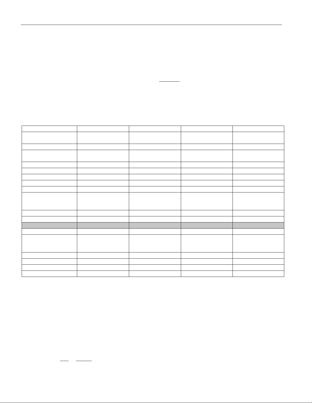
INTERNAL ADDRESS REGISTER MAP Table 2
REGISTER
Configuration Register 40h 0000 1000
Interrupt (INT) Status
Register 1
Interrupt (INT) Status
Register 2
Interrupt (INT) Mask
Register 1
Interrupt (INT) Mask
Register 2
Chassis Intrusion Clear
Register
VID Register 47h 0101 XXXX
Serial Address Register 48h 0010 11XY
VID4 Register 49h 1000 000X
Temperature
Configuration
Register
Test Register 15h 0000 0000
Analog output 19h 1111 1111 Full on
Value RAM 20h-3Dh
Company ID 3Eh 1101 1010 Read only
Stepping 3Fh 0000 0001 Read only
DS1780 INTERNAL
HEX ADDRESS
41h 0000 0000
42h 0000 0000
43h 0000 0000
44h 0000 0000
46h 0000 0000
4Bh 0000 0001
POWER ON VALUE NOTES
DS1780
Bit 7 of this register
clears Chassis Intrusion.
The other bits are
reserved.
The lower 4 bits reflect
the state of
VID0-VID3 pins.
X Reflects state of A1
and Y Reflects A0 state
Bit 0 = VID 4. The rest
are reserved.
Do not alter the
contents of the register.
5 of 28

2-WIRE SERIAL COMMUNICATION WITH THE DS1780 Figure 2
DS1780
OPERATION - Power-on
Applying power to the DS1780 causes a reset of several of the registers. Power-on conditions of the
registers are shown in Table 2 above. Some registers have indeterminate power-on values, such as the
Limit and RAM registers of the Value RAM page, and these are not shown in the table. Upon power-up
the ADC is inactive. Writing Limits into the Value RAM should usually be the first action performed
after power up. The RST pin is bi-directional. It forces RESET at power-on, but can also be pulled low to
force RESET internally.
OPERATION - Resets
The DS1780 features four distinct resetting functions. Each one has a different effect on register contents
and the state of the RST output following the event. Each one is explained below:
Power-on Reset - On POR, all internal logic is reset, and registers are cleared to their default state (see
tables 10.x). Because Value RAM is typically the first area programmed upon power-up, it does not have
a defined state upon POR. Also, on POR, the
(minimum).
A POR occurs every time VDD crosses the voltage level approximately equivalent to the sum of one nchannel threshold (V
) and one p-channel threshold (VTP), on a power-up or power-down condition.
TN
DS1780 SRAM contents get “scrambled” when V
channel VT. Therefore, SRAM contents will always be in a defined state as supply voltage reaches the
minimum spec level of 2.8V, even in a power supply brownout condition.
RST output will be pulled to an active low state for 20 ms
falls below the greater of one n-channel VT or one p-
DD
6 of 28

DS1780
Software Reset - This condition is generated by writing a 1 to bit 4 of the configuration register. It has no
effect on DS1780 register contents. It will however pull the RST output to the active low state for a
duration of 20 ms (minimum). When the RST output goes active, this bit in the configuration register will
clear itself. A Software Reset is only possible if Bit 7 of the INT Mask Register 2 (0x44h) is set to “1”.
Device Initialization - This condition is generated by writing a 1 to bit 7 of the configuration register. It
will clear all registers in DS1780 memory to their default state except the Value RAM (0x20h - 0x3Dh)
and analog output (0x19h). These locations will remain unchanged from their state before the
initialization. This condition has no effect on the RST output. This bit is self-clearing.
Hardware Reset - This condition is generated by some external source pulling the RST pin below
VIN(0) (see DC Electrical Characteristics). The DS1780 will then force the RST signal to remain in the
active low state for >20 ms. It will clear all registers in DS1780 memory to their default state except the
Value RAM (0x20h - 0x3Dh) and analog output (0x19h). These locations will remain unchanged from
their state before the Hardware Reset.
OPERATION - Configuration Register
Control of the DS1780 is provided through the configuration register. The Configuration Register is used
to start and stop the DS1780, enable or disable interrupt output and modes, and provide the initialization
function described above.
Bit 0 of the Configuration Register controls the monitoring loop of the DS1780. Setting Bit 0 low stops
the monitoring loop and puts the DS1780 into a standby mode. 2-Wire Bus communication is still
possible with any register in the DS1780 during the standby mode, however. Additionally, the DS1780
will continue to monitor the RST and CHS inputs while in a standby mode. Setting Bit 0 high starts the
monitoring loop.
Bit 1 of the Configuration Register enables or disables the INT Interrupt output. Setting Bit 1 high
enables the INT output, setting bit 1 low disables the output.
Bit 3 of the Configuration Register is used to clear the INT interrupt output when set high. The DS1780
monitoring function will stop until bit 3 is set low. Interrupt Status register contents will not be affected.
Bit 4 of the Configuration Register is used to initiate a minimum 20 ms RESET signal on the
if the pin is configured for the RESET mode (via bit 7 of the INT Mask Register 2 - 0x44h).
Bit 6 of the Configuration Register is used to reset the Chassis Intrusion (CHS) output pin when set high.
Bit 7 of the Configuration Register is used to start a Configuration Register Initialization when taken
high, as described in the “OPERATION - Resets” section.
RST output
OPERATION - Monitoring Loop
The DS1780 monitoring function is started by doing a write to the Configuration Register and setting the
INT_Clear (Bit 3) low, and Start (Bit 0) high. At this point the INT_Enable (Bit 1) should be set high to
enable interrupts (INT). The DS1780 then performs a “round robin” sampling of the inputs, sampling
each approximately once a second, in the order (corresponding to locations in the Value RAM) shown
below in Table 3. The results of the sampling and conversions can be found in the Value RAM (Table
10.13) and are available at any time.
7 of 28

DS1780
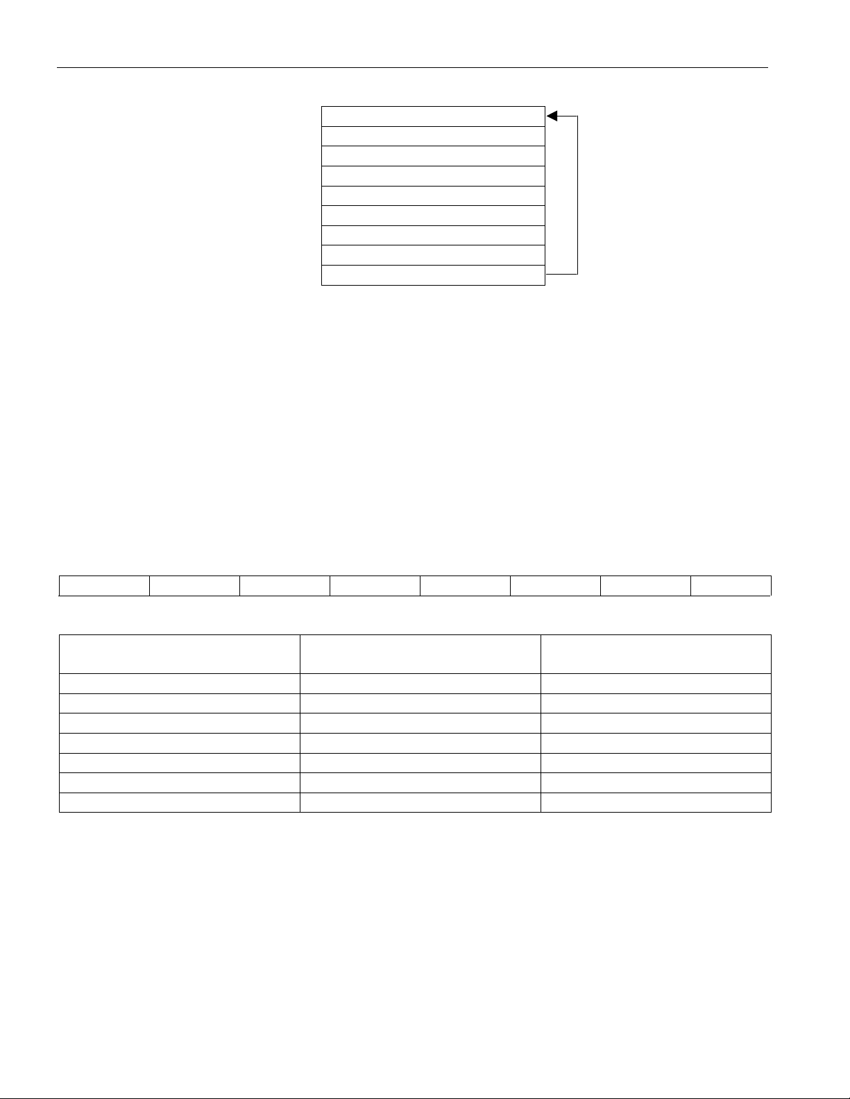
DS1780 MONITORING ORDER Table 3
TEMPERATURE READING
ANALOG +2.5 VS/V
CCP2
ANALOG +12V
ANALOG +5V
ANALOG +3.3V
ANALOG +2.5V
ANALOG +V
CCP1
FAN1
FAN2
If conversions are terminated by either of the methods described in the “OPERATION - Configuration
Register” section, the current “round-robin” loop will be completed and the results stored in RAM.
Monitoring will then terminate. When the monitoring again commences, monitoring always starts with
the temperature reading.
OPERATION - Temperature Data Format
The DS1780 internally converts measured temperature data to a two’s complement data format (in °C).
The host can read the last completed temperature conversion at any time by setting the Internal Address
Register pointer to location 27h, and reading the 8 bits in the register. The format of the data is shown
below in Table 4. The MSb of the register represents the sign bit of the temperature reading. For
Fahrenheit usage, a lookup table or conversion routine must be used.
TEMPERATURE/DATA RELATIONSHIPS Table 4
S262
5
MSb (unit = °C) LSb
TEMPERATURE
+125°C 0111 1101 7Dh
+25°C 0001 1001 19h
+1°C 0000 0001 01h
0°C 0000 0000 00h
-1°C 1111 1111 FFh
-25°C 1110 0111 E7h
-40°C 1101 1000 D8h
4
2
3
2
DIGITAL OUTPUT
(BINARY)
2
2
1
2
2
DIGITAL OUTPUT (HEX)
0
OPERATION - Voltage Data Format
The DS1780 contains inputs for directly monitoring the power supplies typically found in a PC (+12V, 12V, +5V, +3.3V, +2.5V, +V
via an 8-bit Delta-Sigma ADC (Analog-to-Digital Converter), thus allowing for a more accurate means of
measurement since the voltages are referenced to a known value.
). These inputs are scaled internally to a reference source, and converted
CCP
Since these inputs can be greater than VDD, they are not diode protected to the power rails. In addition,
small external series resistors such as 510Ω should be put into the lines driving the DS1780 to prevent
damaging the traces or power supplies should an accidental short connect two power supplies together.
8 of 28

DS1780
The worse such accident would be connecting -12V to +12V; a total of 24V difference, with the series
resistors this would draw a maximum of approximately 24 ma.
The internal scaling factor depends upon the particular input. The +12VIN, +5VIN, +3.3VIN, and +2.5V
IN
inputs are internally scaled such that the nominal value of the respective supply corresponds to 3/4 of full
range, or a decimal count of 192. The approximate resolution is thus equal to:
NOM
LSb (V
NOM
) ≅
V 4/3
256
This is depicted below in Table 5.
VOLTAGE/DATA RELATIONSHIPS FOR POSITIVE ONLY VOLTAGE INPUTS
(+12V
LSb WEIGHTING
ADC RESULT (BASE
, +5VIN, +3.3VIN, and +2.5VIN) Table 5
IN
INPUT PIN +12V
(mV)
PIN VOLTAGE (V) PIN VOLTAGE (V) PIN VOLTAGE (V) PIN VOLTAGE (V)
10)
00000
1 0.063 0.026 0.017 0.013
2 0.125 0.052 0.034 0.026
3 0.188 0.078 0.052 0.039
4 0.25 0.104 0.069 0.052
•
•
•
190 11.875 4.948 3.266 2.474
191 11.938 4.974 3.283 2.487
192 12.0 5.0 3.3 2.5
193 12.063 5.026 3.317 2.513
•
•
•
252 15.75 6.563 4.331 3.281
253 15.813 6.589 4.348 3.294
254 15.875 6.615 4.366 3.307
255 15.938 6.641 4.383 3.32
IN
62.5 26.0 17.2 13.0
•
•
•
•
•
•
+5V
IN
•
•
•
•
•
•
+3.3V
•
•
•
•
•
•
IN
+2.5V
•
•
•
•
•
•
IN
The other two voltage inputs use a slightly different scaling technique, due to the nature of the PC voltage
they are monitoring. Because processor voltage (V
) can vary to 3.6V, the +V
CCP
and +2.5VS/+V
CCP1
CCP1
inputs are internally scaled such that the ADC result is 0h for a 0V input and the maximum value of FFh
is returned for a voltage of 3.60V. This corresponds to an LSb weighting of 14.1 mV.
The inputs can also be used to monitor a negative supply, such as -12V. However, a resistor ladder and
positive reference voltage (V
swings between OV and +3.6V. Assuming the DS1780 +V
input impedance and the V
LSb (R1, R
2
) ≅
3.6
255
REF
+
RR
é
ê
1
R
ë
) must be used (see Figure 1) such that input voltage to the DS1780
REF
and +2.5VS/+V
CCP1
pins have infinite
CCP2
is a perfect supply, then the resolution and range of -12V input are:
21
ù
9 of 28
 Loading...