Dallas Semiconductor DS1673S-5, DS1673S-3, DS1673E-5, DS1673E-3 Datasheet

r
www.dalsemi.com
A
A
A
DS1673
Portable System Controlle
FEATURES
Provides Real Time Clock:
– Counts seconds, minutes, hours, date of
the month, month, day of the week, and
year with leap year compensation valid up
to 2100
– Power control circuitry supports system
power on from day/time alarm
Microprocessor monitor:
– Halts microprocessor during power-fail
– Automatically restarts microprocessor
after power failure
– Monitors pushbutton for external override
– Halts and resets an out of control
microprocessor
NV RAM control:
– Automatic battery backup and write
protection to external SRAM
3-channel, 8-bit analog-to-digital converter
Simple 3-wire interface
+3.0 or +5.0V operation
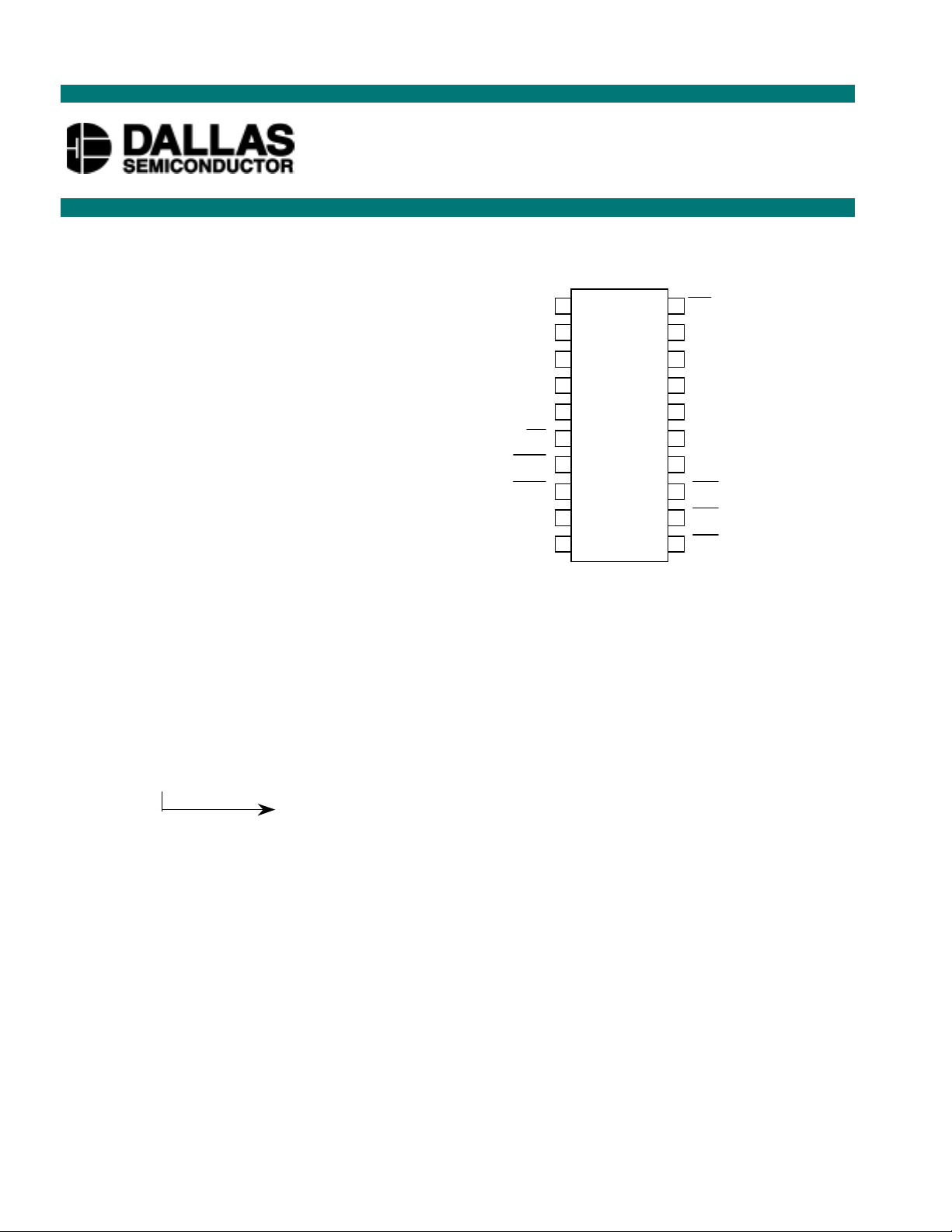
PIN ASSIGNMENT
V
BAT
V
CCO
SCLK
I/O
CS
CEI
CEOL
CEOH
INT
GND
1
2
3
4
5
6
7
8
9
10
20-Pin TSSOP
20-Pin SOIC
20
19
18
17
16
15
14
13
12
11
ST
V
CC
X1
X2
IN0
IN1
IN2
RST
BLE
BHE
ORDERING INFORMATION
DS1673E - X 20-Pin TSSOP
DS1673S - X 20-Pin SOIC
3 +3V operation
5 +5V operation
DESCRIPTION
The Portable System Controller is a circuit which incorporates many of the functions necessary for low
power portable products integrated into one chip. The DS1673 provides a Real Time Clock, NV RAM
controller, microprocessor monitor, and a 3-channel, 8-bit analog-to-digital converter. Communication
with the DS1673 is established through a simple 3-wire interface.
The Real Time Clock (RTC) provides seconds, minutes, hours, day, date, month, and year information
with leap year compensation. The RTC also provides an alarm interrupt. This interrupt works when the
DS1673 is powered by the system power supply or when in battery backup operation so the alarm can be
used to wake up a system that is powered down.
1 of 20 050200

DS1673
Automatic backup and write protection of external SRAM is provided through the V
CEOH pins. The backup energy source used to power the RTC is also used to retain RAM data in the
absence of VCC through the V
pin. The chip enable outputs to RAM ( CEOL and CEOH) are controlled
CCO
, CEOL , and
CCO
during power transients to prevent data corruption.
The microprocessor monitor circuitry of the DS1673 provides three basic functions. First, a precision
temperature-compensated refe rence and comparator circuit monit ors the status of VCC. When an out-oftolerance condition occurs, an internal power-fail signal is generated which forces the reset to the active
state. When VCC returns to an in-tolerance condition, the reset signals are kept in the active state for
250 ms to allow the power supply and processor to stabilize. The second microprocessor monitor
function is pushbutton reset control. The DS1673 debounces a pushbutton input and guarantees an active
reset pulse width of 250 ms. The third function is a watchdog timer. The DS1673 has an internal timer
that forces the reset signals to the active state if the strobe input is not driven low prior to watchdog
time-out.
The DS1673 also provides a 3-channel, 8-bit successive approximation analog-to-digital converter. The
converter has an internal 2.55 volt (typical) reference voltage generated b y an on-board band-gap circuit.
The A/D converter is monotonic (no missing codes) and has an internal analog filter to reduce high
frequency noise.
OPERATION
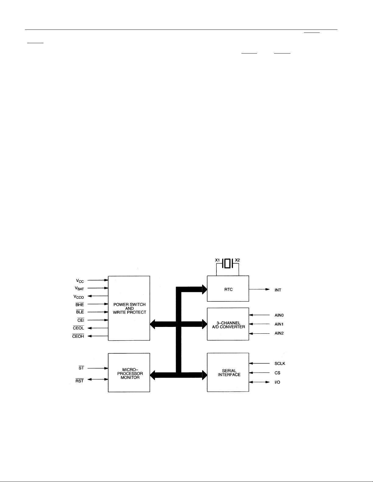
The block diagram in Figure 1 shows the main elements of the DS1673. The following paragraphs
describe the function of each pin.
DS1673 BLOCK DIAGRAM Figure 1
2 of 20

DS1673
SIGNAL DESCRIPTIONS
VCC, GND - DC power is provided to the device on these pins. VCC is the +3.0 volt or +5.0 volt input.
V
(Backup Power Supply) - Battery input for standard 3-volt lithium cell or other energy source.
BAT
SCLK (Serial Clock Input) - SCLK is used to synchronize data movement on the serial interface.
I/O (Data Input/Output) - The I/O pin is the bi-directional data pin for the 3-wire interface.
CS (Chip Select) - The Chip Select signal must be asserted high during a read or a write for
communication over the 3-wire serial interface.
V
(External SRAM Power Supply Output) - This pin is internally connected to VCC when VCC is
CCO
within nominal limits. However, during power-fail V
Switchover occurs when VCC drops below V
CCSW
.
INT (Interrupt Output) - The INT pin is an active high output of the DS1673 that can be used as an
interrupt input to a microprocessor. The INT output remains high as long as the status bit causing the
interrupt is present and the corresponding interrupt-enable bit is set. The INT pin operates when the
DS1673 is powered by VCC or V
BAT
.
is internally connected to the V
CCO
BAT
pin.
CEI (RAM Chip Enable In) - CEI must be driven low to enable the external RAM.
BLE (Byte Low Enable Input) - This pin when driven low activates the CEOL output if CEI is also
driven low.
BHE (Byte High Enable Input) - This pin when driven low activates the CEOH output if CEI is also
driven low.
CEOL (RAM Chip Enable Out Low) – Chip enable output for low order SRAM byte.
CEOH (RAM Chip Enable Out High) – Chip enable output for high order SRAM byte.
ST (Strobe Input) - The Strobe input pin is used in conjunction with the watchdog timer. If the ST pin
is not driven low within the watchdog time period, the
RST (Reset) - The RST pin functions as a microprocessor reset signal. This pin is driven low 1) when
is outside of nominal limits; 2) when the watchdog timer has “timed out”; 3) during the power-up
V
CC
reset period; and 4) in response to a pushbutton reset. The
input. When the
RST pin is driven low, the signal is debounced and timed such that a RST signal of at
RST pin is driven low.
RST pin also functions as a pushbutton reset
least 250 ms is generated. This pin has an internal 47 kΩ pullup resistor.
AIN0, AIN1, AIN2 (Analog Inputs) - These pins are the three analog inputs for the 3-channel analog-todigital converter.
3 of 20

DS1673
X1, X2 - Connections for a standard 32.768 kHz quartz crystal. For greatest accuracy, the DS1673 must
be used with a crystal that has a specified load capacitance of 6 pF. There is no need for external
capacitors or resistors. Note: X1 and X2 are very high impedance nodes. It is recommended that they
and the crystal be guard-ringed with ground and that high frequency signals be kept awa y from the crystal
area. For more information on crystal selection and crystal layout considerations, please consult
Application Note 58, “Crystal Considerations with Dallas Real Time Clocks.”
The DS1673 will not function without a crystal.
POWER-UP/POWER-DOWN CONSIDERATIONS
When VCC is applied to the DS1673 and reaches a level greater than V
device becomes fully accessible after t
When VCC drops below V
, the device is switched over to the V
CCSW
(250 ms typical). Before t
RPU
RPU
BAT
supply.
During power-up, when VCC returns to an in-tolerance condition, the RST pin is kept in the active state
for 250 ms (typical) to allow the power supply and microprocessor to stabilize.
(power-fail trip point), the
CCTP
elapses, all inputs are disabled.
ADDRESS/COMMAND BYTE
The command byte for the DS1673 is shown in Figure 2. Each data transfer is initiated by a command
byte. Bits 0 through 6 specify the address of the registers to be accessed. The MSB (bit 7) is the
Read/Write bit. This bit specifies whether the accessed byte will be read or written. A read operation is
selected if bit 7 is a 0 and a write operation is selected if bit 7 is a one. The address map for the DS1673
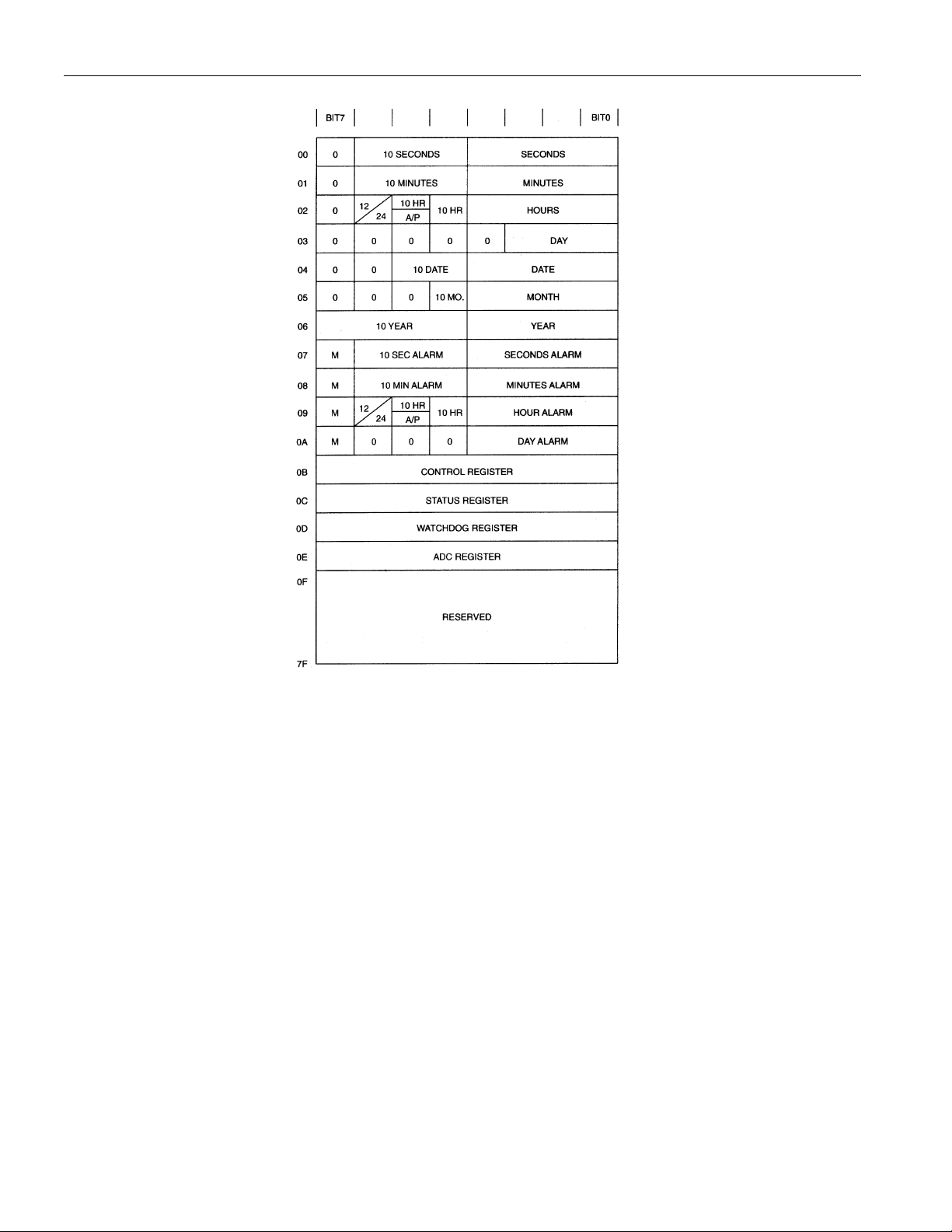
is shown in Figure 3.
ADDRESS/COMMAND BYTE Figure 2
4 of 20

DS1673 ADDRESS MAP Figure 3
DS1673
CLOCK, CALENDAR AND ALARM
The time and calendar information is accessed by reading/writing the appropriate register bytes. Note
that some bits are set to 0. These bits will always read 0 regardless of how they are written. Also note
that registers 0Fh to 7Fh are reserved. These registers will always read 0 regardless of how they are
written. The contents of the time, calendar, and alarm registers are in the Binary-Coded Decimal (BCD)
format. The DS1673 can run in either 12-hour or 24-hour mode. Bit 6 of the hours register is defined as
the 12- or 24-hour mode select bit. When high, the 12-hour mode is selected. In the 12-hour mode, bit 5
is the AM/PM bit with logic 1 being PM. In the 24-hour mode, bit 5 is the second 10-hou r bit (20-23
hours).
The DS1673 also contains a time of day alarm. The alarm registers are located in registers 07h to 0Ah.
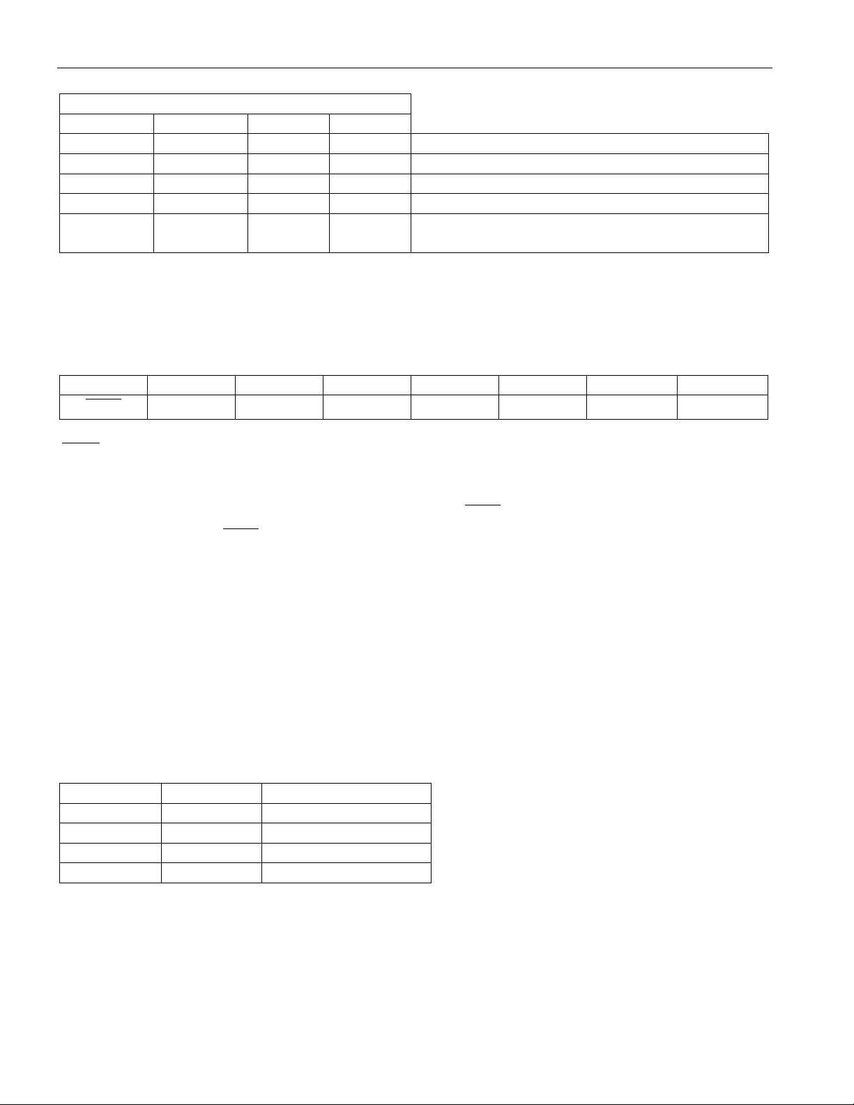
Bit 7 of each of the alarm re gisters are mask bits (see T able 1). When all of the mask bits are logic 0, a n
alarm will occur once per week when the values stored in timekeeping registers 00h to 03h match the
values stored in the time of day alarm registers. An alarm will be generated every day when mask bit of
the day alarm register is set to 1. An alarm will be generated every hour when the day and hour alarm
mask bits are set to 1. Similarly, an alarm will be generated every minute when the day, hour, and minute
alarm mask bits are set to 1. When day, hour, minute, and seconds alarm mask bits are set to 1, an alarm
will occur every second.
5 of 20

DS1673
TIME OF DAY ALARM BITS Table 1
ALARM REGISTER MASK BITS (BIT 7)
SECONDS MINUTES HOURS DAYS
1 1 1 1 Alarm once per second.
0 1 1 1 Alarm when seconds match.
0 0 1 1 Alarm when minutes and seconds match.
0 0 0 1 Alarm when hours, minutes and seconds match.
0 0 0 0 Alarm when day, hours, minutes and seconds
match.
SPECIAL PURPOSE REGISTERS
The DS1673 has two additional registers (control register and status register) that control the Real Time
Clock and interrupts.
CONTROL REGISTER
BIT 7 BIT 6 BIT 5 BIT 4 BIT 3 BIT 2 BIT 1 BIT 0
EOSC
EOSC (Enable Oscillator) - This bit, when set to logic 0 will start the oscillator. When this bit is set to a
logic 1, the oscillator is stopped and the DS1673 is placed into a low-power standby mode with a current
drain of less than 200 nanoamps when in battery back-up mode. When the DS1673 is powered by VCC,
WP AIS1 AIS0 0 0 0 AIE
the oscillator is always on regardless of the status of the EOSC bit; however, the Real Time Clock is
incremented only when EOSC is a logic 0.
WP (Write Protect) - Before an y write operation to the Real Time Clock or any other registers, this bit
must be logic 0. When high, the write protect bit prevents a write operation to any register.
AIS0-AIS1 (Analog Input Select) - These 2 bits are used to determine the analog input for the analog-todigital conversion. Table 2 lists the specific analog input that is selected by these 2 bits.
AIE (Alarm Interrupt Enable) - When set to a logic 1, this bit permits the Interrupt Request Flag
(IRQF) bit in the status register to assert INT. When the AIE bit is set to logic 0, the IRQF bit does not
initiate the INT signal.
ANALOG INPUT SELECTION Table 2
AIS1 AIS0 ANALOG INPUT
0 0 NONE
01 AIN0
10 AIN1
11 AIN2
6 of 20
 Loading...