Dallas Semiconductor DS1731U-T-R, DS1731U, DS1631U, DS1631AU-T-R, DS1631AU Datasheet
...
1 of 14 092502
FEATURES
§ DS1631 and DS1631A Provide ±0.5°C
Accuracy over a 0°C to +70°C Range
§ DS1731 Provides ±1°C Accuracy over a
-10°C to +85°C Range
§ DS1631A Automatically Begins Taking
Temperature Measurements at Power-Up
§ Operating Temperature Range: -55°C to
+125°C (-67°F to +257°F)
§ Temperature Measurements Require No
External Components
§ Output Resolution is User-Selectable to 9,
10, 11, or 12 Bits
§ Wide Power-Supply Range (+2.7V to +5.5V)
§ Converts Temperature-to-Digital Word in
750ms (max)
§ Multidrop Capability Simplifies Distributed
Temperature-Sensing Applications
§ Thermostatic Settings are User-Definable
and Nonvolatile (NV)
§ Data is Read/Written Through 2-Wire Serial
Interface (SDA and SCL Pins)
§ All Three Devices are Available in 8-Pin
mSOP Packages and the DS1631 is Also
Available in a 150mil SO package—see
Table 1 for Ordering Information
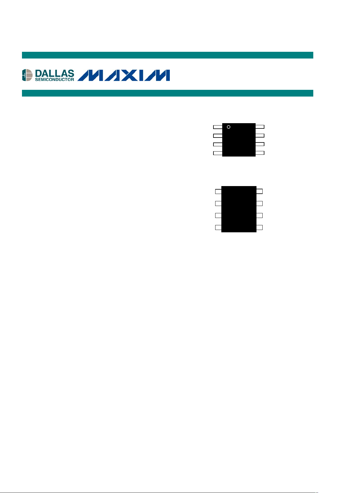
PIN CONFIGURATIONS
DESCRIPTION
The DS1631, DS1631A, and DS1731 digital thermometers provide 9, 10, 11, or 12-bit temperature
readings over a -55°C to +125°C range. The DS1631 and DS1631A thermometer accuracy is ±0.5°C
from 0°C to +70°C with 3.0V £ V
DD
£ 5.5V, and the DS1731 accuracy is ±1°C from -10°C to +85°C with
3.0V £ V
DD
£ 5.5V. The thermostat on all three devices provides custom hysteresis with user-defined trip
points (T
H
and TL). The TH and TL registers and thermometer configuration settings are stored in NV
EEPROM so they can be programmed prior to installation. In addition, the DS1631A automatically
begins taking temperature measurements at power-up, which allows it to function as a stand-alone
thermostat. Communication with the DS1631/DS1631A/DS1731 is achieved through a 2-wire serial
interface, and three address pins allow up to eight devices to be multidropped on the same 2-wire bus.
Pin descriptions for the DS1631/DS1631A/DS1731 are provided in Table 2 and user-accessible registers
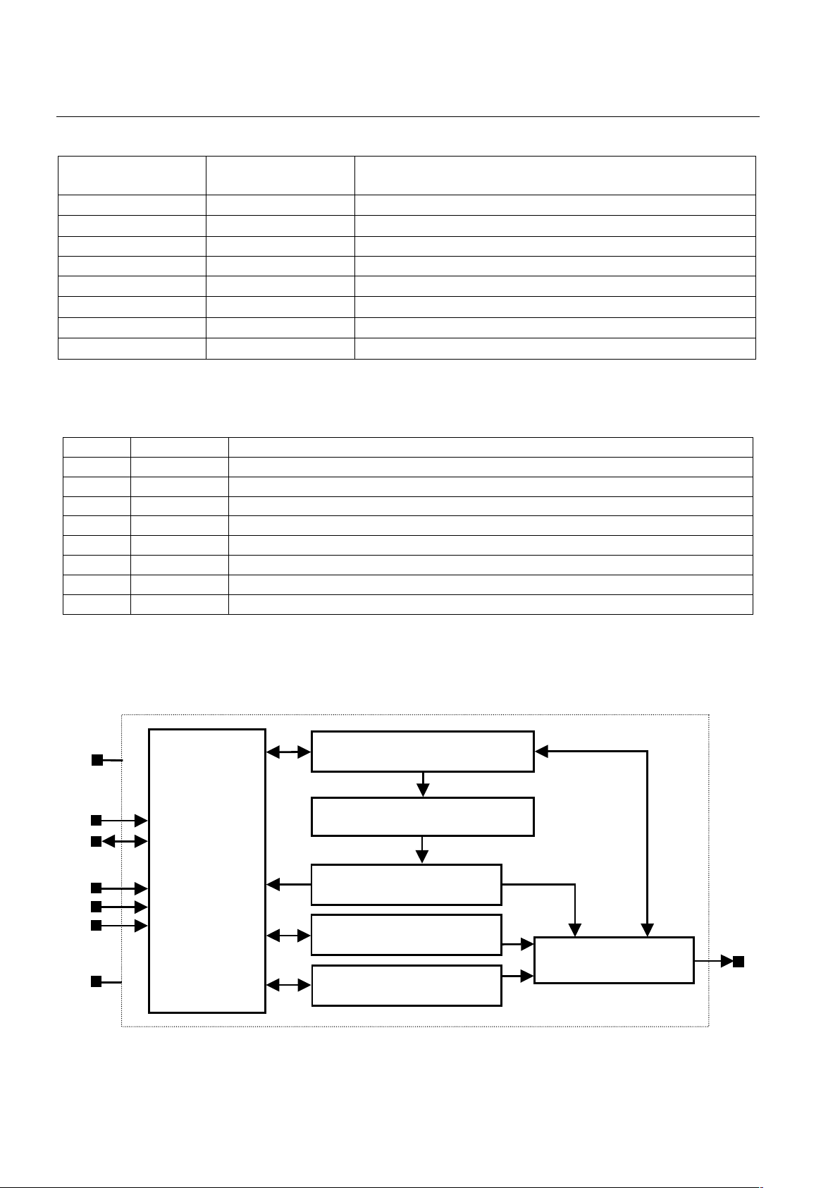
are summarized in Table 3. A functional diagram is shown in Figure 1.
DS1631/DS1631A/DS1731
High-Precision Digital
Thermometer and Thermostat
www.maxim-ic.com
SO (150mil)
(DS1631Z)
SC
L
V
DD
A
0
A
1
A
2
GND
T
OUT
SDA
6
875
3
1
2
4
m
SOP
(DS1631U, DS1631AU, DS1731U)
SC
L
V
DD
A
0
A
1
A
2
GND
T
OUT
SDA
6
875
3
1
2
4
See Table 2 for Pin Descriptions
APPLICATIONS
§ Network Routers and Switches
§ Cellular Base Stations
§ Portable Products
§ Any Space-Constrained Thermally Sensitive
Product

DS1631/DS1631A/DS1731
2 of 14
Table 1. ORDERING INFORMATION
ORDERING
NUMBER
PACKAGE
MARKING
DESCRIPTION
DS1631U D1631
DS1631 in 8-Pin mSOP
DS1631U/T&R D1631
DS1631 in 8-Pin mSOP, 3000-Piece Tape-and-Reel
DS1631Z DS1631Z DS1631 in 150mil 8-Pin SO
DS1631Z/T&R DS1631Z DS1631 in 150mil 8-Pin SO, 2500-Piece Tape-and-Reel
DS1631AU 1631A
DS1631A in 8-Pin mSOP
DS1631AU/T&R 1631A
DS1631A in 8-Pin mSOP, 3000-Piece Tape-and-Reel
DS1731U D1731
DS1731 in 8-Pin mSOP
DS1731U/T&R D1731
DS1731 in 8-Pin mSOP, 3000-Piece Tape-and-Reel
Table 2. DETAILED PIN DESCRIPTION
PIN SYMBOL DESCRIPTION
1 SDA Data Input/Output Pin for 2-Wire Serial Communication Port. Open-Drain.
2 SCL Clock Input Pin for 2-Wire Serial Communication Port.
3T
OUT
Thermostat Output Pin. Push-Pull.
4 GND Ground Pin
5A2Address Input Pin
6A1Address Input Pin
7A0Address Input Pin
8VDDSupply Voltage Pin. +2.7V to +5.5V Power-Supply Pin.
Figure 1. FUNCTIONAL DIAGRAM
CONFIGURATION REGISTER
A
ND CONTROL LOGIC
ADDRESS
AND
I/O CONTROL
A1A2A
0
SCL
SD
A
DIGITAL
COMPARATOR/LOGIC
T
H
REGISTER
TL REGISTER
T
OU
T
TEMPERATURE SENSOR
and DS ADC
TEMPERATURE REGISTER
V
DD
GND

DS1631/DS1631A/DS1731
3 of 14
ABSOLUTE MAXIMUM RATINGS*
Voltage on any Pin Relative to Ground -0.5V to +6.0V
Operating Temperature Range -55°C to +125°C
Storage Temperature Range -55°C to +125°C
Solder Dip Temperature (10s) See IPC/JEDEC J-STD-020A Specification
Reflow Oven Temperature +220°C
* These are stress ratings only and functional operation of the device at these or any other conditions
above those indicated in the operation sections of this specification is not implied. Exposure to absolute
maximum rating conditions for extended periods of time may affect reliability.
DC ELECTRICAL CHARACTERISTICS
(V
DD
= 2.7V to 5.5V; TA = -55°C to +125°C.)
PARAMETER SYMBOL CONDITION MIN MAX UNITS NOTES
Supply Voltage V
DD
2.7 5.5 V 1
0°C to +70°C,
3.0V £ V
DD
£ 5.5V
±0.5
0°C to +70°C,
2.7V £ V
DD
< 3.0V
±1
DS1631, DS1631A
Thermometer Error
T
ERR
-55°C to +125°C ±2
°C 2
-10°C to +85°C,
3.0V £ V
DD
£ 5.5V
±1
-10°C to +85°C,
2.7V £ V
DD
< 3.0V
±1.5
DS1731
Thermometer Error
T
ERR
-55°C to +125°C ±2
°C 2
Low-Level Input
Voltage
V
IL
-0.5 0.3 x V
DD
V
High-Level Input
Voltage
V
IH
0.7 x
V
DD
VDD + 0.3 V
V
OL1
3mA sink current 0 0.4
SDA Low-Level
Output Voltage
V
OL2
6mA sink current 0 0.6
V
Input Current Each
I/O Pin
0.4 < V
I/O
< 0.9V
DD
-10 +10 µA
Temperature
conversion
-55°C to +85°C
1
Temperature
conversion
+85°C to +125°C
1.25
mA
E2 write 400
Active Supply
Current
I
DD
Communication only 110
µA
3
Standby Supply
Current
I
STBY
0°C to +70°C 800 nA 4
V
OH
1mA source current 2.4 V 1
T
OUT
Output Logic
Voltage
V
OL
4mA sink current 0.4 V 1

DS1631/DS1631A/DS1731
4 of 14
AC ELECTRICAL CHARACTERISTICS
(V
DD
= 2.7V to 5.5V; TA = -55°C to +125°C.)
PARAMETER SYMBOL CONDITION MIN TYP MAX UNITS NOTES
9-bit resolution 93.75
10-bit
resolution
187.5
11-bit
resolution
375
Temperature
Conversion Time
t
TC
12-bit
resolution
750
ms
SCL Frequency f
SCL
0 400 kHz
Bus Free Time
Between a STOP and
START Condition
t
BUF
1.3 µs 5
START and Repeated
START Hold Time
from Falling SCL
t
HD:STA
0.6 µs 5, 6
Low Period of SCL t
LOW
1.3 µs 5
High Period of SCL t
HIGH
0.6 µs 5
Repeated START
Condition Setup Time
to Rising SCL
t
SU:STA
0.6 µs 5
Data-Out Hold Time
from Falling SCL
t
HD:DAT
0
0.9 µs 5
Data-In Setup Time to
Rising SCL
t
SU:DAT
100 ns 5
Rise Time of SDA and
SCL
t
R
20 + 0.1C
B
1000 ns 5, 7
Fall Time of SDA and
SCL
t
F
20 + 0.1C
B
300 ns 5, 7
STOP Setup Time to
Rising SCL
t
SU:STO
0.6 µs 5
Capacitive Load for
Each Bus Line
C
B
400 pF
I/O Capacitance C
I/O
10 pF
Input Capacitance C
I
5pF
Spike Pulse Width that
can be Suppressed by
Input Filter
t
SP
050ns
NOTES:
1) All voltages are referenced to GND.
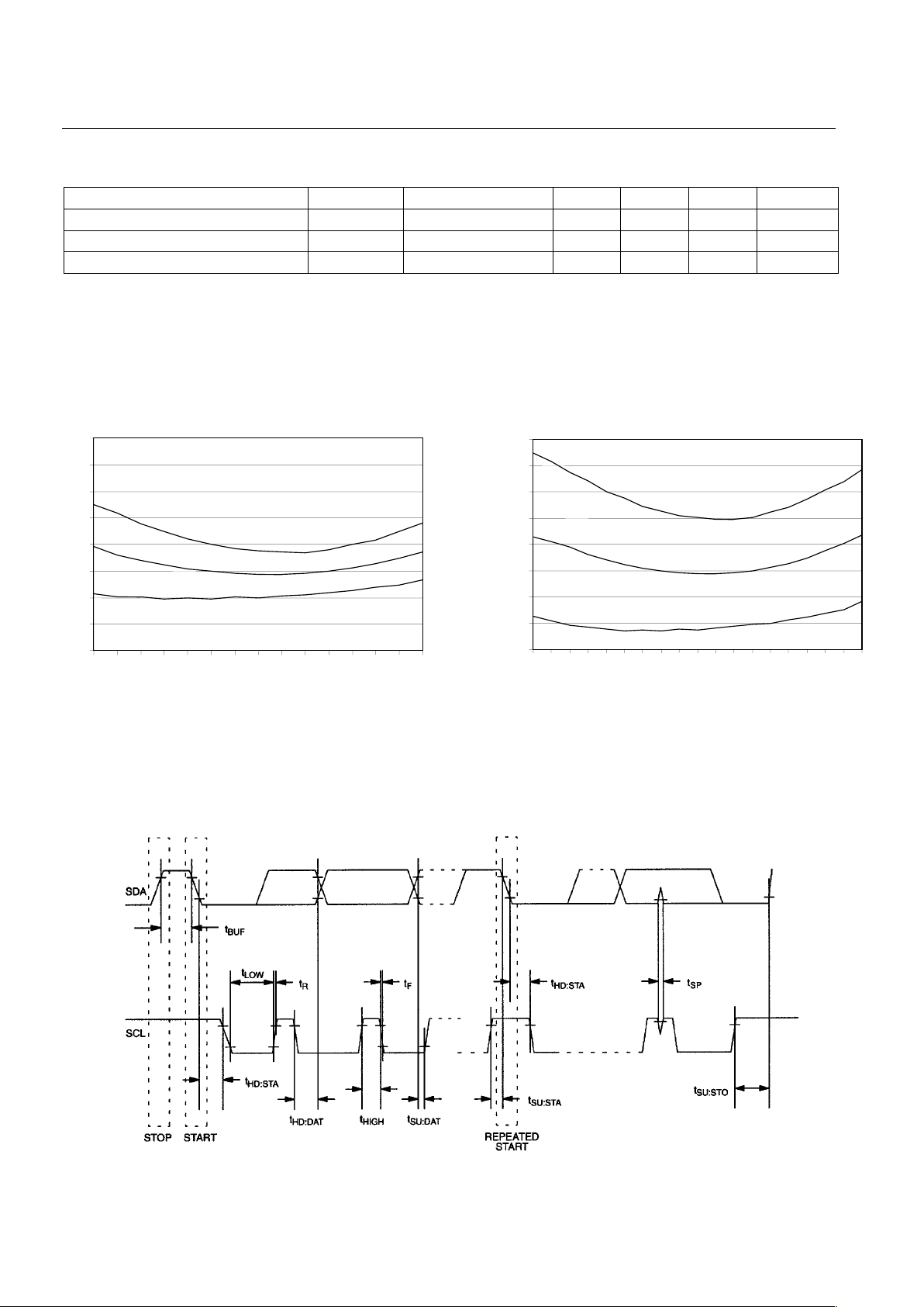
2) See Figure 2 for Typical Operating Curves.
3) Specified with T
OUT
pin open; A0, A1, A2 = 0V or VDD; and f
SCL
³ 2Hz.
4) Specified with temperature conversions stopped; T
OUT
pin open; SDA = VDD; SCL = VDD; and A0, A1,
A2 = 0V or VDD.
5) See Timing Diagram in Figure 3. All timing is referenced to 0.9 x VDD and 0.1 x VDD.
6) After this period the first clock pulse is generated.
7) For example, if CB = 300pF, then tR[min] = tF[min] = 50ns.

DS1631/DS1631A/DS1731
5 of 14
EEPROM AC ELECTRICAL CHARACTERISTICS
(V
DD
= 2.7V to 5.5V; TA = -55°C to +125°C.)
PARAMETER SYMBOL CONDITION MIN TYP MAX UNITS
EEPROM Write Cycle Time t
wr
410ms
EEPROM Writes N
EEWR
-55°C to +55°C 50k Writes
EEPROM Data Retention t
EEDR
-55°C to +55°C 10 Years
Figure 2. TYPICAL OPERATING CURVES
Figure 3. TIMING DIAGRAM
All timing is referenced to 0.9 x VDD and 0.1 x VDD.
-0.8
-0.6
-0.4
-0.2
0
0.2
0.4
0.6
0.8
0 10203040 506070
+3
s
-3
s
Mean
REFERENCE TEMPERATURE (°C)
ERROR (°C)
DS1631/DS1631A
-0.8
-0.6
-0.4
-0.2
0
0.2
0.4
0.6
0.8
-10 0 10 20 30 40 50 60 70 80
+3
s
-3
s
Mean
REFERENCE TEMPERATURE (°C)
ERROR (°C)
DS1731
 Loading...