Dallas Semiconductor DS1624S, DS1624 Datasheet

1 of 16 072099
FEATURES
§ Temperature measurements require no
external components
§ Measures temperatures from -55°C to +125°C
in 0.03125°C increments. Fahrenheit
equivalent is -67°F to +257°F in 0.05625°F
increments
§ Temperature is read as a 13-bit value (two
byte transfer)
§ Converts temperature to digital word in 1
second (max)
§ 256 bytes of E2 memory on board for storing
information such as frequency compensation
coefficients
§ Data is read from/written via a 2-wire serial
interface (open drain I/O lines)
§ Applications include temperature-
compensated crystal oscillators for test
equipment and radio systems
§ 8-pin DIP or SOIC packages
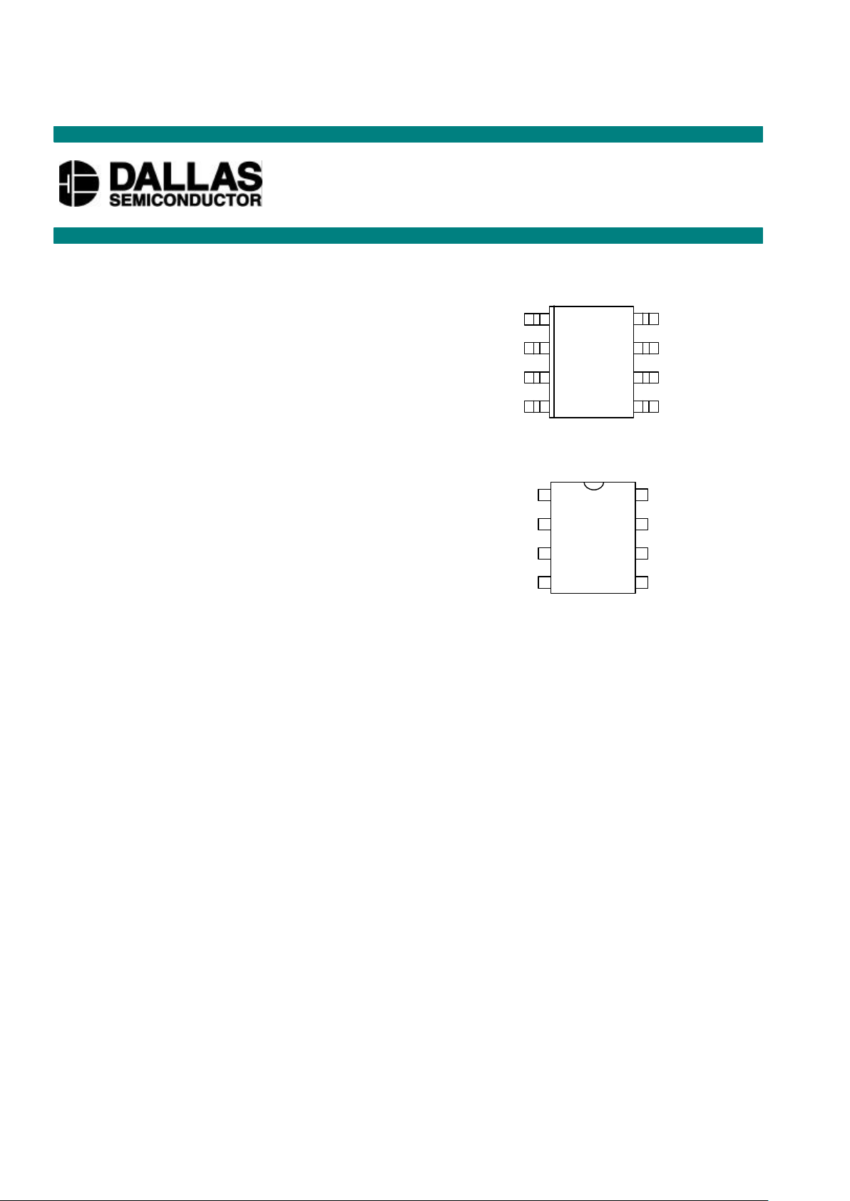
PIN ASSIGNMENT
PIN DESCRIPTION
SDA - 2-Wire Serial Data Input/Output
SCL - 2-Wire Serial Clock
GND - Ground
A0 - Chip Address Input
A1 - Chip Address Input
A2 - Chip Address Input
V
DD
- Digital Power Supply (+3V - +5V)
NC - No Connection
DESCRIPTION
The DS1624 consists of a digital thermometer and 256 bytes of E
2
memory. The thermometer provides
13-bit temperature readings which indicate the temperature of the device. The E
2
memory allows a user to
store frequency compensation coefficients for digital correction of crystal frequency due to temperature.
Any other type of information may also reside in this user space.
DS1624
Digital Thermometer and Memory
www.dalsemi.com
6
312
475
SDA
SCL
NC
GND
VDDA
0
A
1
A2DS1624S 8-PIN SOIC (208 MIL)
See Mech Drawings Section
6
312
4
8
7
5
SDA
SCL
NC
GND
VDDA
0
A
1
A2DS1624 8-PIN DIP (300 MIL)
See Mech Drawings Section

DS1624
2 of 16
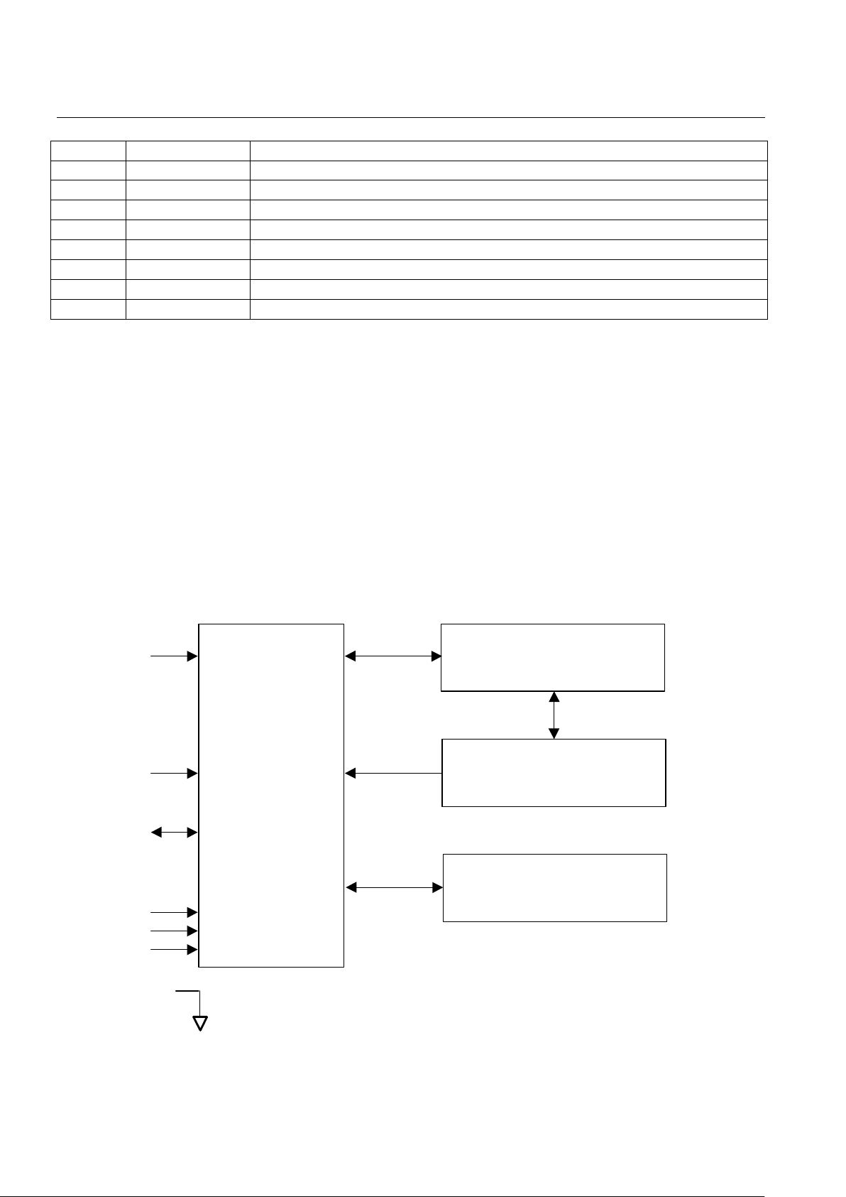
DETAILED PIN DESCRIPTION Table 1
PIN SYMBOL DESCRIPTION
1 SDA Data input/output pin for 2-wire serial communication port.
2 SCL Clock input/output pin for 2-wire serial communication port.
3 NC No connect. No Internal Connection.
4 GND
Ground pin.
5 A2
Address input pin.
6 A1
Address input pin.
7 A0
Address input pin.
8 V
DD
Supply Voltage 2.7V to 5.5V input power pin.
OVERVIEW
A block diagram of the DS1624 is shown in Figure 1. The DS1624 consists of two separate functional
units: 1) a 256–byte nonvolatile E
2
memory, and 2) a direct–to–digital temperature sensor.
The nonvolatile memory is made up of 256 bytes of E
2
memory. This memory may be used to store any
type of information the user wishes; for example, frequency compensation coefficients may be placed in
this memory to allow for compensation of measured frequency depending upon the temperature at which
the measurement is made. These memory locations are accessed through the 2–wire serial bus.
The direct to digital temperature sensor allows the DS1624 to measure the ambient temperature and
report the temperature value in a 13–bit word, with 0.03125°C resolution. The temperature sensor and its
related registers are accessed through the 2–wire serial interface.
DS1624 FUNCTIONAL BLOCK DIAGRAM Figure 1
STATUS REGISTER &
CONTROL LOGIC
TEMPERATURE SENSOR
EEPROM MEMORY (256 BYTES)
ADDRESS
AND
I/O CONTROL
V
DD
SCL
SDAA1A2
A0
GND

DS1624
3 of 16
2-WIRE SERIAL DATA BUS
The DS1624 supports a bi–directional two–wire bus and data transmission protocol. A device that sends
data onto the bus is defined as a transmitter, and a device receiving data as a receiver. The device that
controls the message is called a “master”. The devices that are controlled by the master are “slaves”. The
bus must be controlled by a master device which generates the serial clock (SCL), controls the bus access,
and generates the START and STOP conditions. The DS1624 operates as a slave on the two–wire bus.
Connections to the bus are made via the open–drain I/O lines SDA and SCL. The following bus protocol
has been defined (See Figure 2):
• Data transfer may be initiated only when the bus is not busy.
• During data transfer, the data line must remain stable whenever the clock line is HIGH. Changes in
the data line while the clock line is high will be interpreted as control signals.
Accordingly, the following bus conditions have been defined:
Bus not busy: Both data and clock lines remain HIGH.
Start data transfer: A change in the state of the data line, from HIGH to LOW, while the clock is HIGH,
defines a START condition.
Stop data transfer: A change in the state of the data line, from LOW to HIGH, while the clock line is
HIGH, defines the STOP condition.
Data valid: The state of the data line represents valid data when, after a START condition, the data line
is stable for the duration of the HIGH period of the clock signal. The data on the line must be changed
during the LOW period of the clock signal. There is one clock pulse per bit of data.
Each data transfer is initiated with a START condition and terminated with a STOP condition The
number of data bytes transferred between START and STOP conditions is not limited, and is determined
by the master device. The information is transferred byte–wise and each receiver acknowledges with a
ninth bit.
Within the bus specifications a regular mode (100 KHz clock rate) and a fast mode (400 KHz clock rate)
are defined. The DS1624 works in both modes.
Acknowledge: Each receiving device, when addressed, is obliged to generate an acknowledge after the
reception of each byte. The master device must generate an extra clock pulse which is associated with this
acknowledge bit.
A device that acknowledges must pull down the SDA line during the acknowledge clock pulse in such a
way that the SDA line is stable LOW during the HIGH period of the acknowledge related clock pulse. Of
course, setup and hold times must be taken into account. A master must signal an end of data to the slave
by not generating an acknowledge bit on the last byte that has been clocked out of the slave. In this case,
the slave must leave the data line HIGH to enable the master to generate the STOP condition.

DS1624
4 of 16
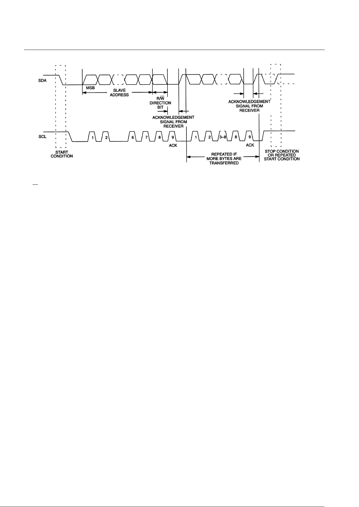
DATA TRANSFER ON 2-WIRE SERIAL BUS Figure 2
Figure 2 details how data transfer is accomplished on the two–wire bus. Depending upon the state of the
R/W bit, two types of data transfer are possible:
1. Data transfer from a master transmitter to a slave receiver. The first byte transmitted by the
master is the slave address. Next follows a number of data bytes. The slave returns an acknowledge
bit after each received byte.
2. Data transfer from a slave transmitter to a master receiver. The first byte (the slave
address) is transmitted by the master. The slave then returns an acknowledge bit. Next follows a
number of data bytes transmitted by the slave to the master. The master returns an acknowledge bit
after all received bytes other than the last byte. At the end of the last received byte, a ‘not
acknowledge’ is returned.
The master device generates all of the serial clock pulses and the START and STOP conditions. A
transfer is ended with a STOP condition or with a repeated START condition. Since a repeated START
condition is also the beginning of the next serial transfer, the bus will not be released.
The DS1624 may operate in the following two modes:
1. Slave receiver mode: Serial data and clock are received through SDA and SCL. After each byte is
received an acknowledge bit is transmitted. START and STOP conditions are recognized as the
beginning and end of a serial transfer. Address recognition is performed by hardware after reception
of the slave address and direction bit.
2. Slave transmitter mode: The first byte is received and handled as in the slave receiver mode.
However, in this mode the direction bit will indicate that the transfer direction is reversed. Serial data
is transmitted on SDA by the DS1624 while the serial clock is input on SCL. START and STOP
conditions are recognized as the beginning and end of a serial transfer.
SLAVE ADDRESS
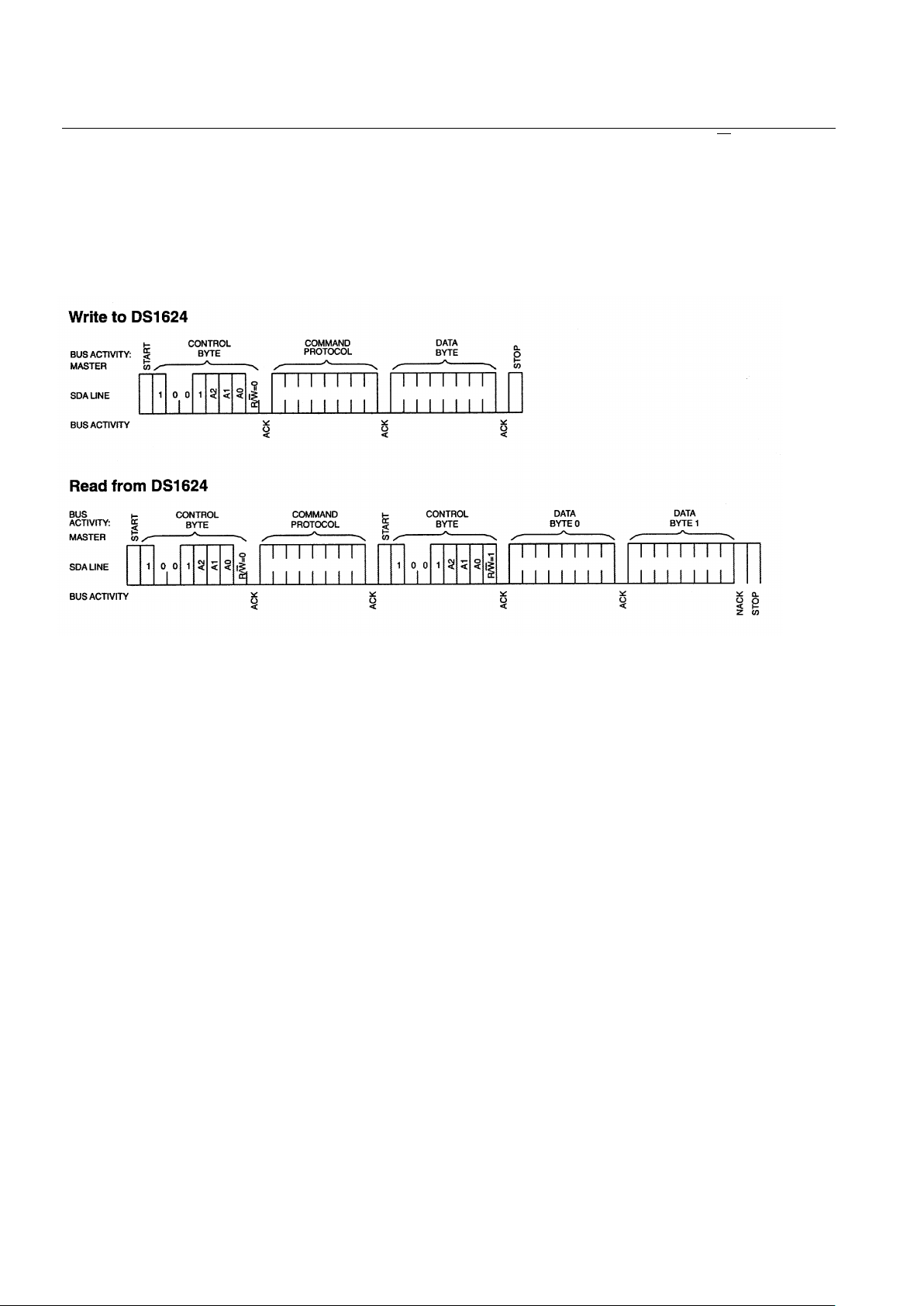
A control byte is the first byte received following the START condition from the master device. The
control byte consists of a four bit control code; for the DS1624, this is set as 1001 binary for read and
write operations. The next three bits of the control byte are the device select bits (A2, A1, A0). They are
used by the master device to select which of eight devices are to be accessed. These bits are in effect the

DS1624
5 of 16
three least significant bits of the slave address. The last bit of the control byte (R/W) defines the
operation to be performed. When set to a “1”, a read operation is selected, when set to a “0”, a write
operation is selected. Following the START condition the DS1624 monitors the SDA bus checking the
device type identifier being transmitted. Upon receiving the 1001 code and appropriate device select bits,
the slave device outputs an acknowledge signal on the SDA line.
2-WIRE SERIAL COMMUNICATION WITH DS1624 Figure 3
OPERATION-MEASURING TEMPERATURE
A block diagram of the DS1624 is shown in Figure 1. The DS1624 measures temperatures through the
use of an on–board proprietary temperature measurement technique. A block diagram of the temperature
measurement circuitry is shown in Figure 4.
The DS1624 measures temperature by counting the number of clock cycles that an oscillator with a low
temperature coefficient goes through during a gate period determined by a high temperature coefficient
oscillator. The counter is preset with a base count that corresponds to –55 °C. If the counter reaches zero
before the gate period is over the temperature register, which is also preset to the –55°C value, is
incremented indicating that the temperature is higher than –55 °C.
At the same time, the counter is preset with a value determined by the slope accumulator circuitry. This
circuitry is needed to compensate for the parabolic behavior of the oscillators over temperature. The
counter is then clocked again until it reaches zero. If the gate period is still not finished, then this process
repeats.
The slope accumulator is used to compensate for the nonlinear behavior of the oscillators over
temperature, yielding a high resolution temperature measurement. This is done by changing the number
of counts necessary for the counter to go through for each incremental degree in temperature. To obtain
the desired resolution, both the value of the counter and the number of counts per °C (the value of the
slope accumulator) at a given temperature must be known.
 Loading...