Dallas Semiconductor DS1616S, DS1616 Datasheet

r
www.dalsemi.com
A
A
A
A
PRELIMINARY
DS1616
Temperature and Three Input
MUX’ed 8-bit Data Recorde
FEATURES
Measures four channels of data:
− Integrated 8-bit temperature sensor,
− Integrated 8-bit Analog-to-Digital Converter
(ADC) with a three input mux for measuring
up to three external sensors
Digital thermometer measures temperature
-40°C to +85°C in 0.5°C increments (-40°F to
+183.2°F in 0.9°F increments)
Digital thermometer provides ±2°C accuracy
Real Time Clock/Calendar in BCD format counts
seconds, minutes, hours, date, month, day of the
week, and year with leap year compensation. The
Real Time Clock is fully Y2K-compliant
Automatically wakes up and measures
temperature and/or ADC data at userprogrammable intervals from 1 to 255 minutes
2048-byte datalog memory
Records long-term temperature histogram in
63 bins with 2.0°C resolution
Records long-term ADC data histogram in 64 bins
with 4-bit resolution/bin (32 mV/bin) for ADC
Channel One
Programmable temperature-high and -low alarm
trip points
Programmable ADC data-high and -low alarm trip
points
Records time stamp and duration when
temperature or ADC Channel 1 Data leaves the
interval specified by the trip points
Two serial interface options: synchronous and
asynchronous
- 3-wire synchronous serial interface
- Asynchronous serial interface compatible with
standard UARTs
Memory partitioned into 32 byte pages for
packetizing data
On-chip 16-bit CRC generator to safeguard data
read operations in asynchronous communications
mode
Unique, factory lasered 64-bit serial number
PIN ASSIGNMENT
V
BAT
X1
X2
GND
NC
COMSEL
INSPEC
OUTSPEC
NC
ST
INT
GND
1
2
3
4
5
6
7
8
9
10
11
12
DS1616 24-Pin DIP (600 mil)
DS1616S 24-Pin SOIC (300 mil)
24
23
22
21
20
19
18
17
16
15
14
13
V
CC
RX
TX
SCLK
I/O
RST
GND
GND
IN3
IN2
IN1
N/C
PIN DESCRIPTION
V
bat
X1 - Crystal Input
X2 - Crystal Output
AINx - Analog in
INSPEC - In-specification Output
OUTSPEC - Out-of-specification Output
INT - Interrupt Output
GND - Digital Ground
AGND - Analog Ground
ST - Start/Status Input
RST - 3-wire Reset Input
I/O - 3-wire Input/Output
SCLK - 3-wire Clock Input
TX - Transmit Output
RX - Receive Input
COMSEL - Communication Select
V
CC
- Battery Supply
- +5V Supply
ORDERING INFORMATION
DS1616 24-Pin DIP
DS1616S 24-Pin SOIC
1 of 29 052300

DS1616
DESCRIPTION
The DS1616 is an integrated temperature/data recorder. It combines a Real Time Clock (RTC),
temperature sensor, and a three input mux’ed 8-bit Analog-to-Digital Converter (ADC). Datalogging is
supported for all four data channels and the and histogram functionality is supported for the temperature
sensor and ADC Channel 1 only. A programmable sample rate feature makes the device ideal for
applications requiring datalogging over short or long time frames.
The RTC provides seconds, minutes, hours, day, date, month, and year information with leap year
compensation, Year 2000 compliance, and also provides an alarm interrupt. Temperature measurement is
provided via integrated thermal technology which can measure temperatures from -40°C to +85°C in
0.5°C increments. An integrated three input mux’ed 8-bit ADC allows the device to record data from
other types of sensors.
The datalog function simply samples data at a user-defined sample rate and writes the data to the Datalog
memory. A total of 2048 bytes of data may be recorded. If only one data channel is selected, a total of
2048 samples can be recorded for that channel. If two channels are enabled, each channel can record
1024 samples. If three or four channels are enabled, each channel can record 512 samples. In the case of
only three channels enabled, the location corresponding to the disabled channel will be 0 to allow the rollover function to work smoothly.
Histogram functionality is provided for the Thermal Sensor and ADC Channel 1, and is implemented by
sampling the data and then incrementing the count value in a data bin associated with that value. The
DS1616 provides 63 2-byte data bins in 2°C increments for the temperature channel and 64 2-byte data
bins in 4-bit resolution steps (32mV/bin) for the ADC Data Channel 1. The sampling rate can be
programmed at intervals ranging from once per minute to once every 255 minutes.
The DS1616 provides programmable high- and low-temperature alarm trip points that allow the device to
monitor whether the temperature stays within desired limits. Likewise, high- and low- trip points can be
programmed for the ADC data. The device can drive an interrupt or status pin if the ADC data falls
outside of the programmable limits. The Temperature Sensor and Channel 1 of the ADC can also have
any event that falls outside of the programmed limits recorded with a time and date stamp and the
duration of the out-of-limits condition for additional analysis in the Alarm Memory. The DS1616 can be
programmed to begin sampling data via a pushbutton input or via a command sent over the serial
interface by a host machine.
A 64-bit serial number is available for unique product identification and tracking.
OVERVIEW
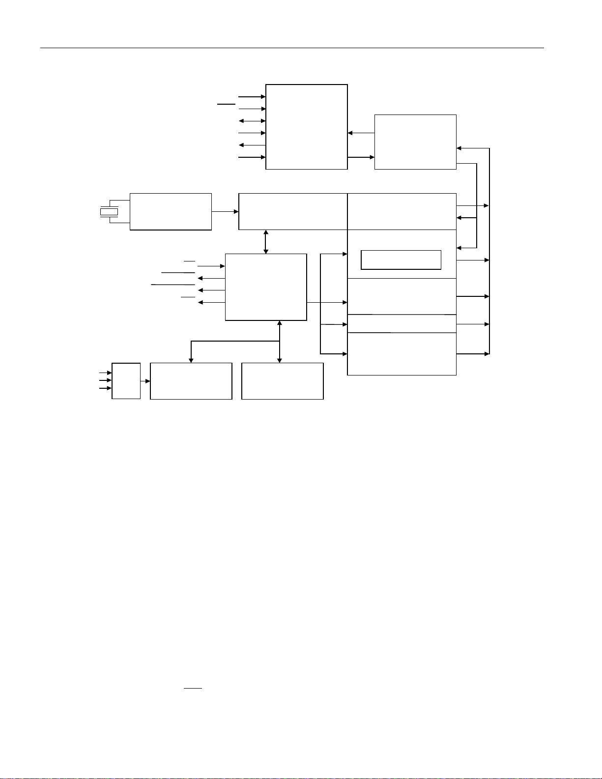
The block diagram in Figure 1 shows the relationship between the major control and memory sections of
the DS1616. The device has six major data components: 1) Real Time Clock and control blocks, 2)
32-byte User NV RAM with 64-bit lasered serial number, 3) 96 bytes of alarm event/duration memory, 4)
128 bytes of temperature histogram RAM, 5) 128 bytes of ADC Channel 1 data histogram RAM, and 6)
2048 bytes of datalog memory. All memory is arranged in a single linear address space.
2 of 29

DS1616 Block Diagram Figure 1
SCLK
RST
I/O
COMSEL
Tx
Rx
X1
OSCILLATOR
AND
X2
DIVIDER
ST
INSPEC
OUTSPEC
INT
INTERNAL RTC
AND CONTROL
REGISTERS
CONTROL
LOGIC
SERIAL
INTERFACE
DS1616
MEMORY
FUNCTION
CONTROL
RTC AND CONTROL
REGISTERS
USER NVRAM
OPTIONAL
SERIAL NUMBER
ALARM TIME STAMP
AND DURATION
LOGGING MEMORY
HISTOGRAM MEMORY
DATALOG MEMO R Y
AIN
3 TO 1
MUX
A/D
CONVERTER
TEMPERATURE
SENSOR
SIGNAL DESCRIPTIONS
The following paragraphs describe the function of each pin.
VCC - VCC is a +5 volt input supply. Communication with the DS1616 can take place only when V
connected to a +5 volt supply.
- Battery input for standard lithium cell or other energy source. All functions of the DS1616 with the
V
bat
exception of the serial interface circuitry are powered by V
powered by VCC when VCC > V
. If a battery or other energy source is not used, V
bat
when VCC < V
bat
. All functions are
bat
should be
bat
connected directly to GND.
GND - GND connections are not internally connected, so all GND connections must be connected
directly to ground.
AGND - Analog ground should be connected directly to digital ground externally to eliminate ground
noise and potential differences.
CC
is
COMSEL (Communication Select Input) - This pin determines whether serial communication is
asynchronous or synchronous. When pulled high to VCC, communication is synchronous and will take
place via the SCLK, I/O, and
RST pins. When COMSEL is tied to ground, asynchronous communication
utilizing the TX and RX pins is selected. If this pin is floated, the DS1616 will operate in the
asynchronous communications mode since the COMSEL pin has a weak internal pulldown resistor.
3 of 29

DS1616
Tx (Transmit Output) - Transmit output of the asynchronous serial interface. Tx is tri-stated whenever
VCC < V
bat
.
Rx (Receive Input) - Receive input of the asynchronous serial interface.
SCLK (3-Wire Serial Clock Input) - The SCLK pin is the serial clock input for the 3-wire synchronous
communications channel.
I/O (3-Wire Input/Output) - The I/O pin is the data Input/Output signal for the 3-wire synchronous
communications channel.
RST (3-Wire Reset Input) - The RST pin is the communications reset pin for the 3-wire synchronous
communications channel.
NTI (Interrupt Output) - The INT pin is an open drain active low output that can be connected to an
interrupt input of a microprocessor. The
INT output remains low as long as the status bit causing the
interrupt is present and the corresponding interrupt-enable bit is set.
INSPEC (Open Drain In-Specification Output) - This pin, in conjunction with the OUTSPEC pin, is
used to signal the status of the operation and data of the DS1616.
OUTSPEC (Open Drain Out-of-Specification Output) - This pin, in conjunction with the INSPEC pin,
is used to signal the status of the operation and data of the DS1616.
ST (Start/Status Button Input) - The ST pin provides two functions. First, when enabled as the datalog
start source (SE bit in Control 1 register is a logic 1), the ST pin is used to instruct the DS1616 to begin
recording data based on the programmed start delay and data sample rate. The ST pin must be held low
for at least 0.5 seconds for a datalog mission to begin.
Secondly, the ST pin can be used to poll the status of the recorded data. After datalogging has begun, the
ST pin instructs the DS1616 to report the status of the recorded data via the INSPEC and OUTSPEC pins.
AIN1, AIN2, AIN3 (Analog Inputs) - The AINx pins are the mux’ed inputs to the ADC.
X1, X2 - Connections for a standard 32.768 kHz quartz crystal, Daiwa part number DT-26S or
equivalent. For greatest accuracy, the DS1616 must be used with a crystal that has a specified load
capacitance of 6 pF. There is no need for external capacitors or resistors. Note: X1 and X2 are very high
impedance nodes. It is recommended that they and the crystal be guard-ringed with ground and that high
frequency signals be kept away from the crystal area. For more information on crystal selection and
crystal layout considerations, please consult Application Note 58, “Crystal Considerations with Dallas
Real Time Clocks.”
NC (No Connect) - These pins should be left unconnected or tied to ground.
4 of 29

DS1616
MEMORY
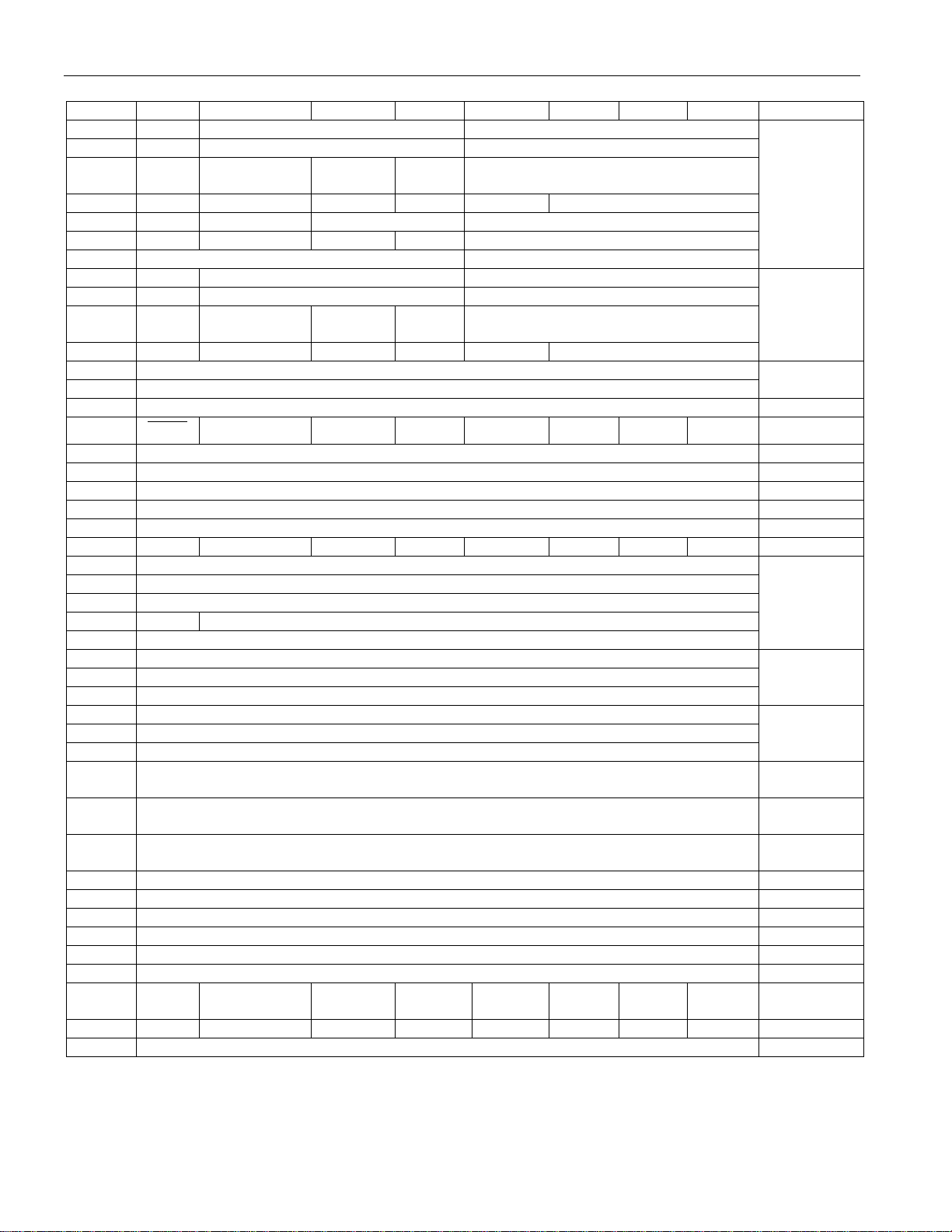
The memory map in Figure 2a shows the general organization of the DS1616. As can be seen in the
figure, the device is segmented into 32-byte pages. Pages 0 and 1 contain the Real Time Clock and
Control registers (see Figure 2b for more detail). The User NV RAM resides in page 2. Pages 17 to 19
are assigned to storing the alarm time stamps and durations and pages 64 to 71 are reserved for histogram
memory. The data logging memory covers pages 128 to 191. Memory pages 3 to 16, 20 to 63, 68 to 127,
and 192 and up are reserved for future extensions.
The end user can write only to the Real Time Clock and Control registers and the User NV RAM. The
rest of the memory map is read-only from the end user’s perspective.
DS1616 MEMORY MAP Figure 2a
0000H
to 003FH
0040H
to 0005FH
0060H
to 0217H
0218H
to 021FH
00220H
to 027FH
0280H
to 07FFH
0800H
to 087FH
0880H
to 08FFH
0900H
to 0FFFH
1000H
to 17FFH
1800H
and higher
RTC and Control Registers pages 0 and 1
User NV RAM page 2
page 3
(Reserved for Future Extensions)
Serial Number page 16
Alarm Time Stamps and Durations page 17
(Reserved for Future Extensions) page 20 - 63
Temperature Histogram (63 Bins of 2 Bytes Each) page 64
ADC Channel 1 Data Histogram (64 Bins of 2 Bytes Each) page 68
(Reserved for Future Extensions) page 72 - 127
Datalog Memory (64 pages) page 128
(Reserved for Future Extensions) page 192 and
to page 16
(excluding last
8 bytes of
page 16)
(last 8 bytes)
to page 19
to page 67
to page 71
to page 191
higher
5 of 29

DS1616 RTC AND CONTROL PAGE Figure 2b
Addr. Bit 7 Bit 6 Bit 5 Bit 4 Bit 3 Bit 2 Bit 1 Bit 0 Function
00 0 10 Seconds Single Seconds
01 0 10 Minutes Single Minutes
02 0 12/24 10 h
A/P
030 0 000 Day Of Week
04 0 0 10 Date Single Date
05 Y2K 0 0 10 m. Single Months
06 10 Years Single Years
07 MS 10 Seconds Alarm Single Seconds Alarm
08 MM 10 Minutes Alarm Single Minutes Alarm
09 MH 12/24 10 ha.
A/P
0A MD 0 0 0 0 Day Of Week Alarm
0B Low Temperature Threshold
0C High Temperature Threshold
0D Number Of Minutes Between Temperature Conversions Sample Rate
0E
0F (reads 00h) Reserved
10 (reads 00h) Reserved
11 Current Temperature Temperature
12 Start Delay Register (LSB) Start Delay
13 Start Delay Register (MSB) Start Delay
14 DR MEM CLR MIP SIP LOBAT TLF THF ALMF Status 1
15 Minutes
16 Hours
17 Date
18 Y2K Month
19 Year
1A Low Byte
1B Medium Byte
1C High Byte
1D Low Byte
1E Medium Byte
1F High Byte
20 Current ADC Channel 1 Data Sensor Input
21 Current ADC Channel 2 Data Sensor Input
22 Current ADC Channel 3 Data Sensor Input
23 Low ADC Channel 1 Data Threshold ADC Data
24 High ADC Channel 1 Data Threshold Ch1 Alarm
25 Low ADC Channel 2 Data Threshold ADC Data
26 High ADC Channel 2 Data Threshold Ch2 Alarm
27 Low ADC Channel 3 Data Threshold ADC Data
28 High ADC Channel 3 Data Threshold Ch3 Alarm
29 0 CS0
2A 0 ALF1 AHF1 ALF2 AHF2 ALF3 AHF3 0 Status 2
2B-3F (reads 00h) Reserved
EOSC
CLR 0 SE RO TLIE THIE AIE Control 1
CS1
(Temp)
(ADC 1)
10 h Single Hours
10 h.
alm.
CS2
(ADC 2)
CS3
(ADC 3)
Single Hours Alarm
ALIE AHIE 0 Control 2
RealTime
Clock
Registers
RealTime
Clock
Alarm
Temperature
Alarm
Start
Time
Stamp
Current
Samples
Counter
Total
Samples
Counter
DS1616
1
2
3
6 of 29

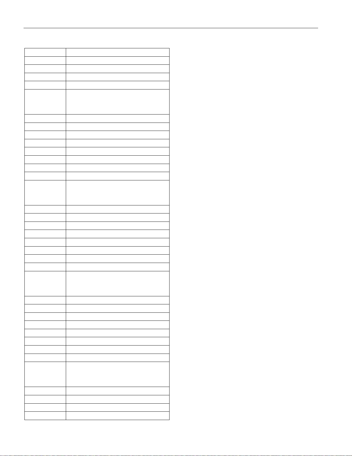
DS1616 ALARM TIME STAMPS AND DURATIONS FOR THE THERMAL
SENSOR AND ADC CHANNEL 1 Figure 2c
Address Register
220 T1 Low Samples Counter LSB
221 T1 Low Samples Counter
222 T1 Low Samples Counter MSB
223 T1 Low Duration
224
↓
233
234 T6 Low Samples Counter LSB
235 T6 Low Samples Counter
236 T6 Low Samples Counter MSB
237 T6 Low Duration
238 T1 High Samples Counter LSB
239 T1 High Samples Counter
23A T1 High Samples Counter MSB
23B T1 High Duration
23C
↓
24B
24C T6 High Samples Counter LSB
24D T6 High Samples Counter
24E T6 High Samples Counter MSB
24F T6 High Duration
250 D1 Low Samples Counter LSB
251 D1 Low Samples Counter
252 D1 Low Samples Counter MSB
253 D1 Low Duration
254
↓
263
264 D6 Low Samples Counter LSB
265 D6 Low Samples Counter
266 D6 Low Samples Counter MSB
267 D6 Low Duration
268 D1 High Samples Counter LSB
269 D1 High Samples Counter
26A D1 High Samples Counter MSB
26B D1 High Duration
26C
↓
27B
27C D6 High Samples Counter LSB
27D D6 High Samples Counter
27E D6 High Samples Counter MSB
27F D6 High Samples Duration
↓
↓
↓
↓
DS1616
7 of 29

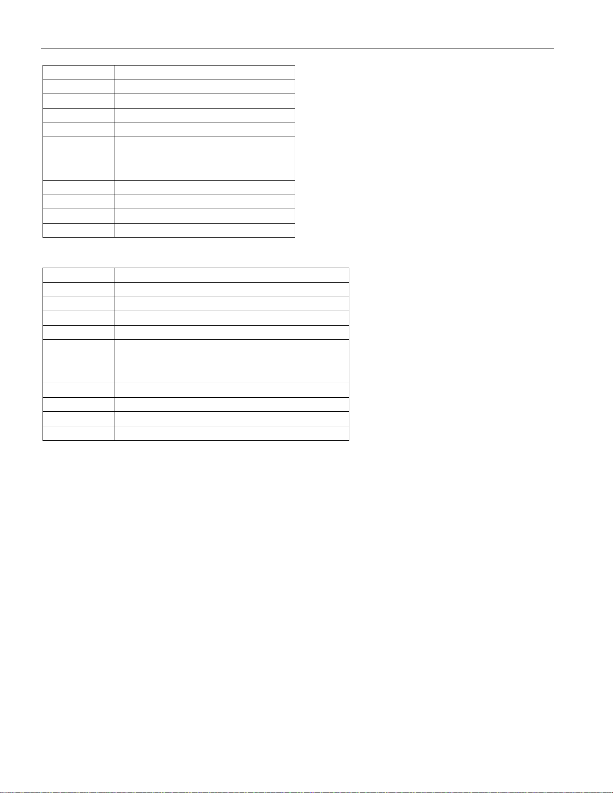
DS1616 TEMPERATURE HISTOGRAM DATA BINS Figure 2d
Address Register
800 -40°C Data Bin (LSB)
801 -40°C Data Bin (MSB)
802 -38°C Data Bin (LSB)
803 -38°C Data Bin (LSB)
804
↓
87B
87C 82°C Data Bin (LSB)
87D 82°C Data Bin (MSB)
87E 84°C Data Bin (LSB)
87F 84°C Data Bin (MSB)
↓
DS1616 ADC DATA HISTOGRAM DATA BINS Figure 2e
Address Register
880 Channel 1 Code 00-03h Data Bin (LSB)
881 Channel 1 Code 00-03h Data Bin (MSB)
882 Channel 1 Code 04-07h Data Bin (LSB)
883 Channel 1 Code 04-07h Data Bin (MSB)
884
↓
8FB
8FC Channel 1 Code F8-FBh Data Bin (LSB)
8FD Channel 1 Code F8-FBh Data Bin (MSB)
8FE Channel 1 Code FC-FFh Data Bin (LSB)
8FF Channel 1 Code FC-FFh Data Bin (MSB)
↓
DS1616
THERMAL SENSOR
The key to temperature monitoring in the DS1616 is an integrated thermal sensor. The thermal sensor
can measure temperature from -40°C to +85°C in 0.5°C increments (Fahrenheit equivalent is -40°F to
+183.2°F in 1.8°F increments). The thermal sensor provides an accuracy of ±2°C.
The thermal sensor is enabled by setting the CS0 bit of the Control 2 register to a logic 1. If the CS0 bit
is a logic 0, the thermal sensor will not be activated during a datalogging mission or for an individual
Read Data command. If CS0 = 0, the value in the Current Temperature register will be 11111111b.
The format of temperature data is defined such that the temperature value is maintained in a single byte of
data. Table 1 illustrates the format of the temperature data byte format. The values of T[7..0] range from
00000000b (for -40°C) to 11111010b (for +85°C). Each increment in the value of T[7..0] represents an
increase in temperature of 0.5°C. The following simple formula can be used to translate the temperature
data byte value into degrees Celsius:
°C = 0.5(T[7..0]) - 40
8 of 29

DS1616
TEMPERATURE DATA BYTE FORMAT Table 1
MSb LSb
T7 T6 T5 T4 T3 T2 T1 T0
When a datalog mission has been initiated and the thermal sensor is enabled (CS0=1), the DS1616
provides temperature recording at regular intervals. However, the device also allows for immediate
temperature sensing upon a user’s command when the device is not currently on a datalog mission and
the thermal sensor is enabled (CS0=1). This is accomplished by issuing the Read Data command to the
DS1616 over the serial interface.
The most recently recorded temperature value is written to the Current Temperature register, regardless of
whether that value was recorded from a datalog mission or from the issuance of the Read Data command.
The status of the contents of this register is provided by the Data Ready (DR) bit in the Status 1 register.
If DR is a logic 1, the data is valid. If DR is a logic 0, the data may not be reliable. If CS0 in the Control
2 register is a 0 such that the thermal sensor is disabled, the value in the Current Temperature register will
be 11111111b. The Read Data command will not output this byte of data.
During a datalog mission, the DR bit is cleared to a logic 0 when a temperature conversion has been
initiated and is set to a logic 1 upon the completion of the conversion. Likewise, the DR bit is cleared
immediately after the Read Data command is issued and is set to a logic 1 upon the completion of the
conversion. The Read Data command will only read the values in the current temperature/ADC data that
have been enabled by the CSx[03] bits in the control 2 register.
ANALOG-TO-DIGITAL CONVERTER (ADC)
The DS1616 contains an integrated 8-bit ADC with a 3 to 1 input mux to allow multiple sensors to be
monitored. An on-chip voltage reference is also provided by an integrated band gap circuit (2.04V ±3%).
The ADC input voltage must not be greater than the battery voltage.
An analog-to-digital conversion is the process of assigning a digital value to an analog input voltage.
This code represents the input value as a fraction of the full scale voltage (FSV) range. Thus the FSV
range is then divided by the ADC into 256 codes (8 bits). The FSV range is bounded by an upper limit
equal to the reference voltage and the lower limit which is ground. The 2.04V (typical) bandgap
reference provides a resolution of 8mV between codes.
An input voltage equal to the reference voltage converts to FFh while an input voltage equal to ground
converts to 00h. The relative linearity of the ADC is ±0.5 LSB.
When a datalog mission has been initiated and one or more of the Analog Inputs are enabled (CS[1-3] =
1), the DS1616 provides data conversion and recording at regular intervals. However, the device also
allows for immediate data conversion upon a user’s command when the device is not currently
performing a conversion and one or more of the Analog Inputs are enabled (CS[1-3] = 1). This is
accomplished by issuing the Read Data command to the DS1616 over the serial interface.
The most recently recorded data value is written to the Current Data register that corresponds to the
analog channel(s) that is(are) enabled, regardless of whether that value was recorded from a datalog
mission or from the issuance of the Read Data command. The status of the contents of this register is
provided by the Data Ready (DR) bit in the Status 1 register. If DR is a logic 1, the data is valid. If DR is
a logic 0, the data may not be reliable. If a channel is not enabled, CS[1-3] is a logic 0, the contents of
the corresponding Current Data register will be 00000000b and not outputted when a Read Data
command is issued.
9 of 29
 Loading...