Dallas Semiconductor DS1615S, DS1615 Datasheet

r
www.dalsemi.com
DS1615
Temperature Recorde
FEATURES
Digital thermometer measures temperature
-40°C to +85°C in 0.5°C increments (-40°F
to +183.2°F in 0.9°F increments)
Digital thermometer provides ±2°C accuracy
Real Time Clock/Calendar in BCD format
counts seconds, minutes, hours, date, month,
day of the week, and year with leap year
compensation (Y2K compatible)
Automatically wakes up and measures
temperature at user-programmable intervals
from 1 to 255 minutes
Logs up to 2048 consecutive temperature
measurements in read-only nonvolatile
memory
Records long-term temperature histogram in
63 bins with 2.0°C resolution
Programmable temperature-high and
temperature-low alarm trip points
Two serial interface options: synchronous and
asynchronous
- 3-wire synchronous serial interface
- Asynchronous serial interface compatible
with standard UARTs
Memory partitioned into 32-byte pages for
packetizing data
On-chip 16-bit CRC generator to safeguard
data read operations in asynchronous
communications mode
Unique, factory lasered and tested 64-bit
serial number
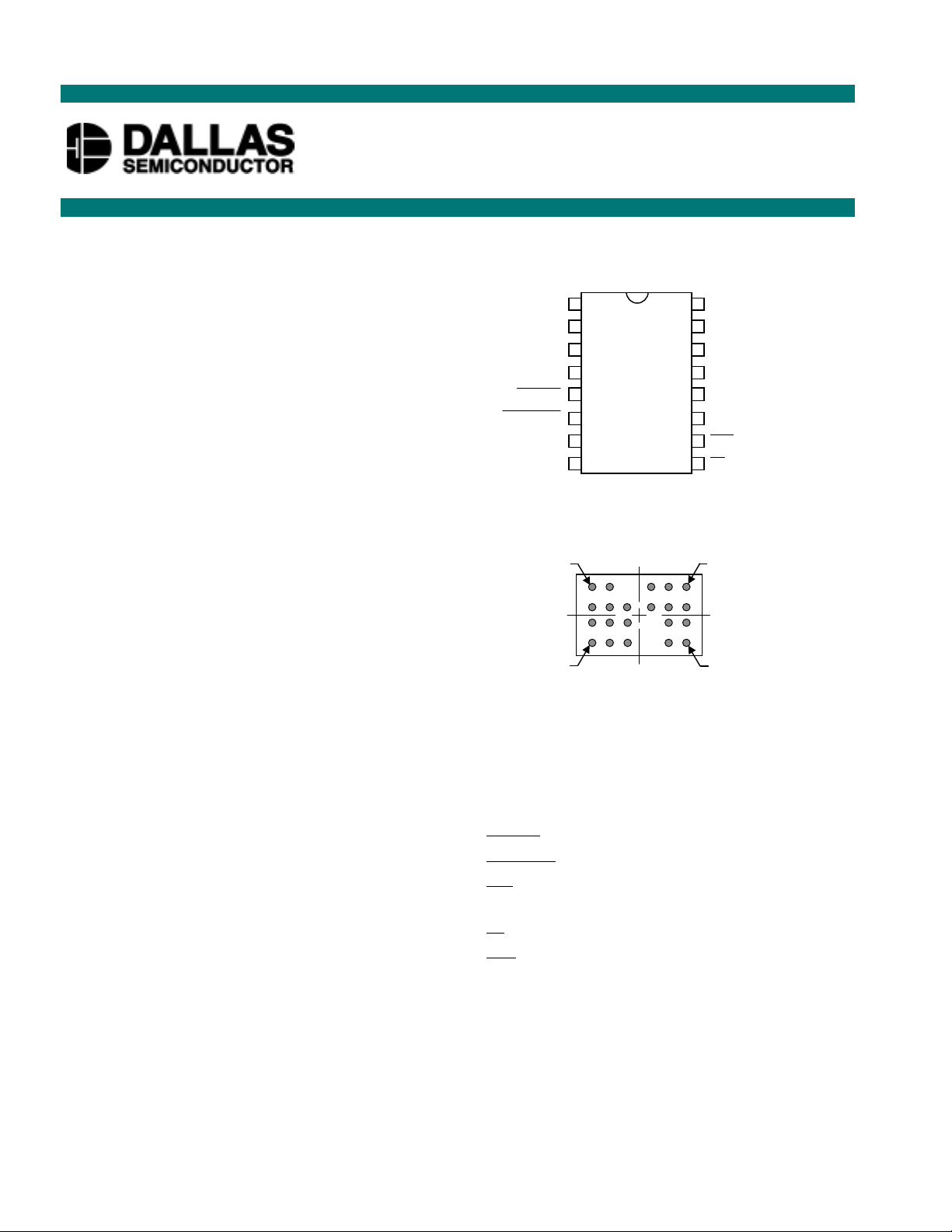
PIN ASSIGNMENT
V
INSPEC
OUTSPEC
GND
1
BAT
2
X1
3
X2
4
NC
5
6
7
INT
8
DS1615 16-Pin DIP
DS1615S 16-Pin SOIC (300 mil)
Top View
DS1615X Flip Chip Package
Bottom View
16
15
14
13
12
11
10
9
V
CC
COMSEL
RX
TX
SCLK
I/O
RST
ST
BUMP 1BUMP 5
BUMP 17BUMP 21
PIN DESCRIPTION
V
- Battery Supply
bat
X1 - Crystal Input
X2 - Crystal Output
NC - No Connect
INSPEC - In-specification Output
OUTSPEC - Out-of-specification Output
INT - Interrupt Output
GND - Ground
ST - Start/Status Input
RST - 3-wire Reset Input
I/O - 3-wire Input/Output
SCLK - 3-wire Clock Input
TX - Transmit Output
RX - Receive Input
COMSEL - Communication Select
- +5V Supply
V
CC
1 of 24 052400

DS1615
ORDERING INFORMATION
DS1615 16-Pin DIP
DS1615S 16-Pin SOIC
DS1615X Flip Chip Package
**For more information of Flip Chip Packaging, go to www.dalsemi.com to the Released Data Sheets
section and select Chip Scale and Flip Chip Package Data Index.
DS1615S 16 -Pin SOIC
DESCRIPTION
The DS1615 is an integrated temperature recorder that combines a real time clock with temper ature data
logging and histogram capabilities. It has been designed for applications that require temperature
profiling over a given period of time. A programmable sampling rate feature makes the device ideal for
applications requiring temperature monitoring over short or long time frames. The integrated Real Time
Clock (RTC) provides seconds, minutes, hours, day, date, month, and year information with leap year
compensation and also provides an alarm interrupt. Temperature measurement is provided via integrated
thermal technology which can measure temperatures from -40°C to +85°C in 0.5°C increments.
The DS1615 is a powerful data recording device, providing both a datalog of sampled temperature values
over time and a histogram of temperature. The datalog function simply samples the temperature at a user
defined sample rate and writes the data to the Temperature Datalog memory. Up to 2048 datalog samples
may be recorded. Histogram functionality is implemented by sampling the temperature and then
incrementing the count value in a data bin associated with that temperature. The DS1615 provides
63, 2-byte data bins in 2°C increments. The user can program data sampling for both data logging and for
histogram tabulation at intervals ranging from once per minute to once every 255 minutes.
The DS1615 also supports programmable high and low temperature alarm trip points that allow the
device to monitor whether the temperature stays within desired limits. The device can drive an interrupt
or status pin if the temperature falls outside of the programmable limits. The DS1615 can be
programmed to begin sampling data via a pushbutton input or via a command sent over the serial
interface with a host machine.
The DS1615 also provides a 64-bit serial number which is useful for product identification and tracking.
OVERVIEW
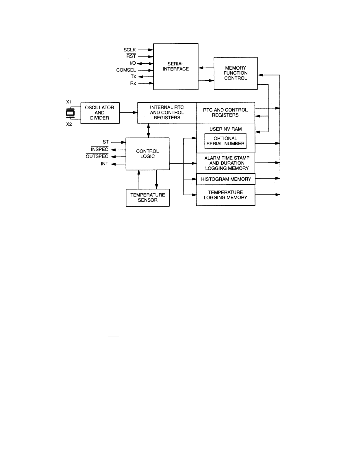
The block diagram in Figure 1 shows the relationship between the major control and memory sections of
the DS1615. The device has five major data components: 1) Real Time Clock and control block, 2)
32-byte User NV RAM with 64-bit lasered serial number, 3) 96 bytes of Alarm event/dur ation memory,
4) 128 bytes of histogram RAM, and 5) 2048 bytes of datalog memory. All memory is arranged in a
single linear address space.
2 of 24

DS1615 BLOCK DIAGRAM Figure 1
DS1615
SIGNAL DESCRIPTIONS
The following paragraphs describe the function of each pin.
VCC- VCC is a +5V input supply. Communication with the DS1615 can take place only when VCC is
connected to a +5V supply.
V
- Battery input for standard lithium cell or other energy source. All functions of the DS1615 with the
bat
exception of the serial interf ac e circui try are powered by V
by VCC when VCC > V
. If a battery or other energy source is not used, the V
bat
directly to GND.
GND - Ground
COMSEL (Communication Select Input) - This pin determines whether serial communication is
asynchronous or synchronous. When pulled high to V
place via the SCLK, I/O, and RST pins. When COMSEL is tied to ground, asynchronous communication
utilizing the TX and RX pins is selected. If this pin is floated, the DS1615 will operate in the
asynchronous communications mode since the COMSEL pin has a weak internal pulldown resistor.
Tx (Transmit Output) - Transmit output of the asynchronous serial interface. Tx is tri-stated whenev er
V
CC
< V
bat
.
when VCC< V
bat
, communication is synchronous and will take
CC
. All functions are powered
bat
pin should be connected
bat
Rx (Receive Input) - Receive input of the asynchronous serial interface.
SCLK (3-wire Serial Clock Input) - The SCLK pin is the serial clock input for the 3-wire synchronous
communications channel.
3 of 24

DS1615
I/O (3-wire Input/Output) - The I/O pin is the data Input/Output signal for the 3-wire synchronous
communications channel.
RST (3-wire Reset Input) - The RST pin is the communications reset pin for the 3-wire synchronous
communications channel.
INT (Interrupt Output) - The INT pin is an open drain active low output that can be connected to an
interrupt input of a microprocessor. The INT output remains low as long as the status bit causing the
interrupt is present and the corresponding interrupt-enable bit is set.
INSPEC (Open Drain In-Specification Output) - This pin, in conjunction with the OUTSPEC pin, is
used to signal the status of the operation and data of the DS1615.
OUTSPEC (Open Drai n Out-of-Sp ecification Out-p ut) - This pin, in conjunction with the INSPEC pin,
is used to signal the status of the operation and data of the DS1615.
ST (Start/Status Button Input) - The ST pin provides two functions. First, when enabled as the datalog
start source (SE bit in Control register is a logic 1), the ST pin is used to instruct the DS1615 to begin
recording temperature data based on the programmed start delay and data sample rate. The ST pin must
be held low for at least 0.5 seconds for a datalog mission to begin. An external pullup resistor should be
connected to this pin.
Secondly, the ST pin can be used to poll the status of the recorded data. After datalogging has b e gun, the
ST pin instructs the DS1615 to report the status of the recorded data via the INSPEC and OUTSPEC pins.
X1, X2 - Connections for a standard 32.768 kHz quartz crystal, Daiwa part number DT-26S or
equivalent. For greatest accuracy, the DS1615 must be used with a crystal that has a specified load
capacitance of 6 pF. There is no need for external capacitors or resistors. Note: X1 and X2 are very hi gh
impedance nodes. It is recommended that they and the crystal be guard-ri n ged with ground and th at high
frequency signals be kept away from the crystal area. For more information on crystal selection and
crystal layout considerations, please consult Application Note 58, Crystal Considerations with Dallas
Real Time Clocks.
NC (No Connect) - This pin should be left unconnected.
MEMORY
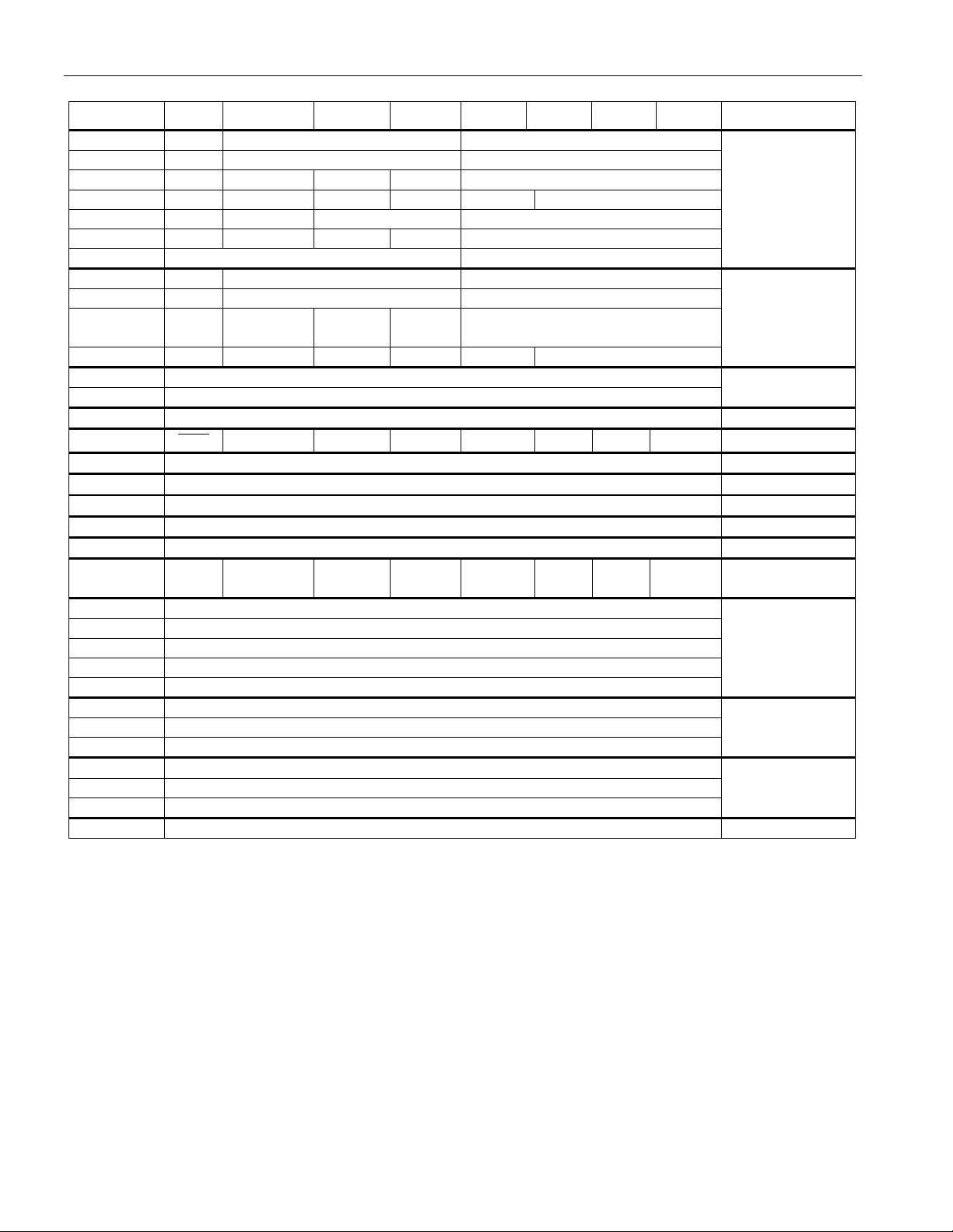
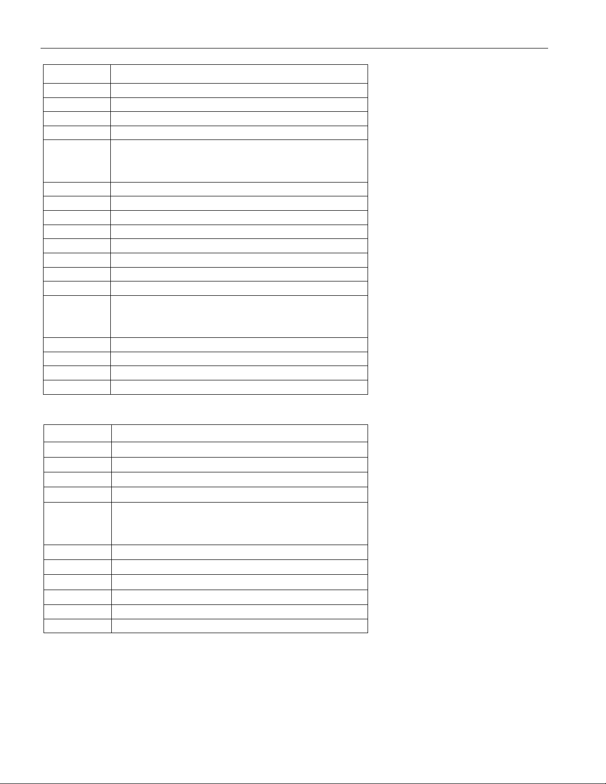
The memory map in Figure 2a shows the general organization of the DS1615. As can be seen in the
figure, the device is segmented into 32 byte pages. Pages 0 and 1 contain the Real Time Clock and
Control registers (see Figure 2b for more detail). The User NV RAM resides in p age 2. Pages 17 to 19
are assigned to storing the alarm time stamps and durations. The temperature histogram bins begin at
page 64 and use up four pages. The temperature logging memor y covers pages 128 to 191. Memory
pages 1, 3 to 16, 20 to 63, 68 to 127, and 192 and up are reserved for future extensions.
The end user can write only to the Real Time Clock and Control registers and the User NV RAM. The
rest of the memory map is read-only from the end users perspective.
4 of 24

DS1615 MEMORY MAP Figure 2a
ADDRESS
AND HIGHER
0000H
TO 001FH
0020H
TO 003FH
0040H
TO 005FH
0060H
TO 0217H
0218H
TO 021FH
00220H
TO 027FH
0280H
TO 07FFH
0800H
TO 087FH
0880H
TO 0FFFH
1000H
TO 17FFH
1800H
RTC AND CONTROL REGISTERS PAGE 0
(RESERVED FOR FUTURE EXTENSIONS)
ALARM TIME STAMPS AND DURATIONS
(RESERVED FOR FUTURE EXTENSIONS) PAGES 20 - 63
TEMPERATURE HISTOGRAM (63 BINS OF 2 BYTES EACH)
(RESERVED FOR FUTURE EXTENSIONS) PAGES 68 - 127
TEMPERATURE DATALOG MEMORY (64 PAGES)
(RESERVED FOR FUTURE EXTENSIONS)
(RESERVED) PAGE 1
USER NV RAM PAGE 2
PAGE 3
TO PAGE 16
(EXCLUDING LAST
8 BYTES OF
PAGE 16)
SERIAL NUMBER
PAGE 16
(LAST 8 BYTES)
PAGE 17
TO PAGE 19
PAGE 64
TO PAGE 67
PAGE 128
TO PAGE 191
PAGE 192 AND
HIGHER
DS1615
5 of 24

DS1615 RTC AND CONTROL PAGE Figure 2b
ADDRESS BIT 7 BIT 6 BIT 5 BIT 4 BIT 3 BIT 2 BIT 1 BIT 0 FUNCTION
00 0 10 Seconds Single Seconds
01 0 10 Minutes Single Minutes
02 0 12/24 10 h A/P 10 h Single Hours
03 0 0 0 0 0 Day Of Week
04 0 0 10 Date Single Date
05 0 0 0 10 m. Single Month
06 10 Years Single Years
07 MS 10 Seconds Alarm Single Seconds Alarm
08 MM 10 Minutes Alarm Single Minutes Alarm
09 MH 12/24 10 h A/P 10 h
Single Hours Alarm
alm
0A MD 0 0 0 0 Day Of Week Alarm
0B Low Temperature Threshold
0C High Temperature Threshold
0D Number Of Minutes Between Temperature Conversions Sample Rate
0E
EOSC
CLR 0 SE RO TLIE THIE AIE
0F (reads 00h) Reserved
10 (reads 00h) Reserved
11 Current Temperature Temperature
12 Start Delay Register (LSB) Start Delay
13 Start Delay Register (MSB) Start Delay
14 TR MEM
MIP SIP LOBAT TLF THF ALMF Status
CLR
15 Minutes
16 Hours
17 Date
18 Month
19 Year
1A Low Byte
1B Medium Byte
1C High By t e
1D Low Byte
1E Medium Byte
1F High Byte
20-3F (Read 00H) Reserved
Real Time Clock
Registers
Real Time Alarm
Clock
Temperature
Alarm
Control
Start Time Stamp
Current Samples
Counter
Total Samples
Counter
DS1615
6 of 24

DS1615 ALARM TIME STAMPS AND DURATIONS Figure 2c
ADDRESS REGISTER
220 T1 Low Samples Counter LSB
221 T1 Low Samples Counter
222 T1 Low Samples Counter MSB
223 T1 Low Duration
224
↓
24B
24C T12 Low Samples Counter LSB
24D T12 Low Samples Counter
24E T12 Low Samples Counter MSB
24F T12 Low Duration
250 T1 High Samples Counter LSB
251 T1 High Samples Counter
252 T1 High Samples Counter MSB
253 T1 High Duration
254
↓
27B
27C T12 High Samples Counter LSB
27D T12 High Samples Counter
27E T12 High Samples Counter MSB
27F T12 High Duration
↓
↓
DS1615
DS1615 HISTOGRAM MEMORY Figure 2d
ADDRESS REGISTER
800
801
802
803
804
↓
879
87A
87B
87C
87D
87E Reserved (00h)
87F Reserved (00h)
-40°C Data Bin (LSB)
-40°C Data Bin (MSB)
-38°C Data Bin (LSB)
-38°C Data Bin (MSB)
↓
82°C Data Bin (LSB)
82°C Data Bin (MSB)
84°C Data Bin (LSB)
84°C Data Bin (MSB)
7 of 24

DS1615
THERMAL SENSOR
The key to temperature monitoring in the DS1615 is an integrated thermal sensor. The thermal sensor
can measure temperature from -40°C to +85°C in 0.5°C increments (Fahrenheit equivalent is -40°F to
+183.2°F in 0.9°F increments). The thermal sensor provides an accuracy of ±2°C.
The format of temperature data is defined such that the temperature value is maintained in a single byte of
data. Table 1 illustrates the format of the temperature data byte format. Th e values of T[ 7..0] ran ge fro m
00000000b (for -40°C) to 11111010b (for 85°C). Each increment in the value of T[7..0] represents an
increase in temperature of 0.5°C . The following simple fo rmula can be used to translate the temperature
data byte value into degrees Celsius:
°C = 0.5(T[7..0]) - 40
TEMPERATURE DATA BYTE FORMAT Table 1
MSb LSb
T7 T6 T5 T4 T3 T2 T1 T0
When a datalog mission has been initiated, the DS1615 provides temperature recording at regular
intervals. However, the device also allows for immediate temperature sensing upon a users command
when the device is not currently on a datalog mission. This is accomplished by issuing the Read
Temperature command to the DS1615 over the serial interface.
The most recently recorded temperature value is written to the Current Temperature register, regardless of
whether that value was recorded f rom a datalog mission or from the issuan ce of the Read Temperature
command. The status of the contents of this register is provided by the Temperature Ready (TR) bit in
the Status register. If TR is a logic 1, the data is valid. If TR is a logic 0, the data may not be reliable.
During a datalog mission, the TR bit is cleared to a logic 0 when a temperature conversion has been
initiated and is set to a logic 1 upon the completion of the conversion. Likewise, the TR bit is cleared
immediately after the Read Temperature command is issued and is set to a logic 1 upon the completion of
the conversion.
DATA LOGGING
When the DS1615 datalogging function is enabled, the device is said to be on a datalo g mission until the
data-logging is stopped.
During a datalog mission, temperature samples are successively written to the Temperature Datalog
memory pages. These memory pages are located at addresses 1000h to 17FFh. The first sample is
written to address location 1000h. The second sample is written to address location 1001h. Likewise, the
address is incremented with each additional data sample. A total of 2048 registers hav e been reserved for
datalog data.
A datalog mission can be initiated via two different methods; by a host instruction over the serial
interface or by a pushbutton input. When the SE bit in the Control register is cleared to a logic 0, the start
function of the
mission. When the SE bit is set to a logic 1, the pushbutton method of starting a mission is enabled.
Under this mode of operation, the DS1615 will begin a datalog mission when a non-zero value has been
written to the Sample Rate register and then the
ST pin is disabled and writing any non-zero value to the Sample Rate register will start a
ST pin has been held low for at least 0.5 seconds.
The sample rate during a datalog mission is equal to the value written to the Sample Rate register
multiplied by one minute. Writing a 0 to the MIP bit in the Status register completes the mission.
8 of 24
 Loading...