Dallas Semiconductor DS1609S, DS1609 Datasheet

DS1609
Dual Port RAM
DS1609
020499 1/7
FEATURES
• Totally asynchronous 256–byte dual port memory
• Multiplexed address and data bus keeps pin count
low
• Dual port memory cell allows random access with
minimum arbitration
• Each port has standard independent RAM control sig-
nals
• Fast access time
• Low power CMOS design
• 24–pin DIP or 24–pin SOIC surface mount package
• Both CMOS and TTL compatible
• Operating temperature of –40°C to +85°C
• Standby current of 100 nA @ 25°C makes the device
ideal for battery backup or battery operate applications.
PIN ASSIGNMENT
DS1609S
24–PIN SOIC (300 MIL)
V
CC
OE
B
CE
B
WE
B
AD0
B
AD1
B
AD2
B
AD3
B
AD4
B
AD5
B
AD6
B
AD7
B
AD7
A
AD6
A
AD5
A
AD4
A
AD3
A
AD2
A
AD1
A
AD0
A
WE
A
CE
A
OE
A
GND
PORT A
DS1609
24–PIN DIP (600 MIL)
PORT A PORT B
V
CC
OE
B
CE
B
WE
B
AD0
B
AD1
B
AD2
B
AD3
B
AD4
B
AD5
B
AD6
B
AD7
B
AD7
A
AD6
A
AD5
A
AD4
A
AD3
A
AD2
A
AD1
A
AD0
A
WE
A
CE
A
OE
A
GND
1
2
3
4
5
6
7
8
9
10
11
12
24
23
22
21
20
19
18
17
16
15
14
13
1
2
3
4
5
6
7
8
9
10
11
12
24
23
22
21
20
19
18
17
16
15
14
13
See Mech. Drawings
Section
See Mech. Drawings
Section
PORT B
PIN DESCRIPTION
AD0–AD7 – Port address/data
CE – Port enable
WE – Write enable
OE – Output enable
V
CC
– +5 volt supply
GND – Ground
DESCRIPTION
The DS1609 is a random access 256–byte dual port
memory designed to connect two asyncronous address/data buses together with a common memory element. Both ports have unrestricted access to all
256 bytes of memory, and with modest system discipline no arbitration is required. Each port is controlled
by three control signals: output enable, write enable,
and port enable. The device is packaged in plastic
24–pin DIP and 24–pin SOIC. Output enable access
time of 50 ns is available when operating at 5 volts.

DS1609
020499 2/7
OPERATION – READ CYCLE
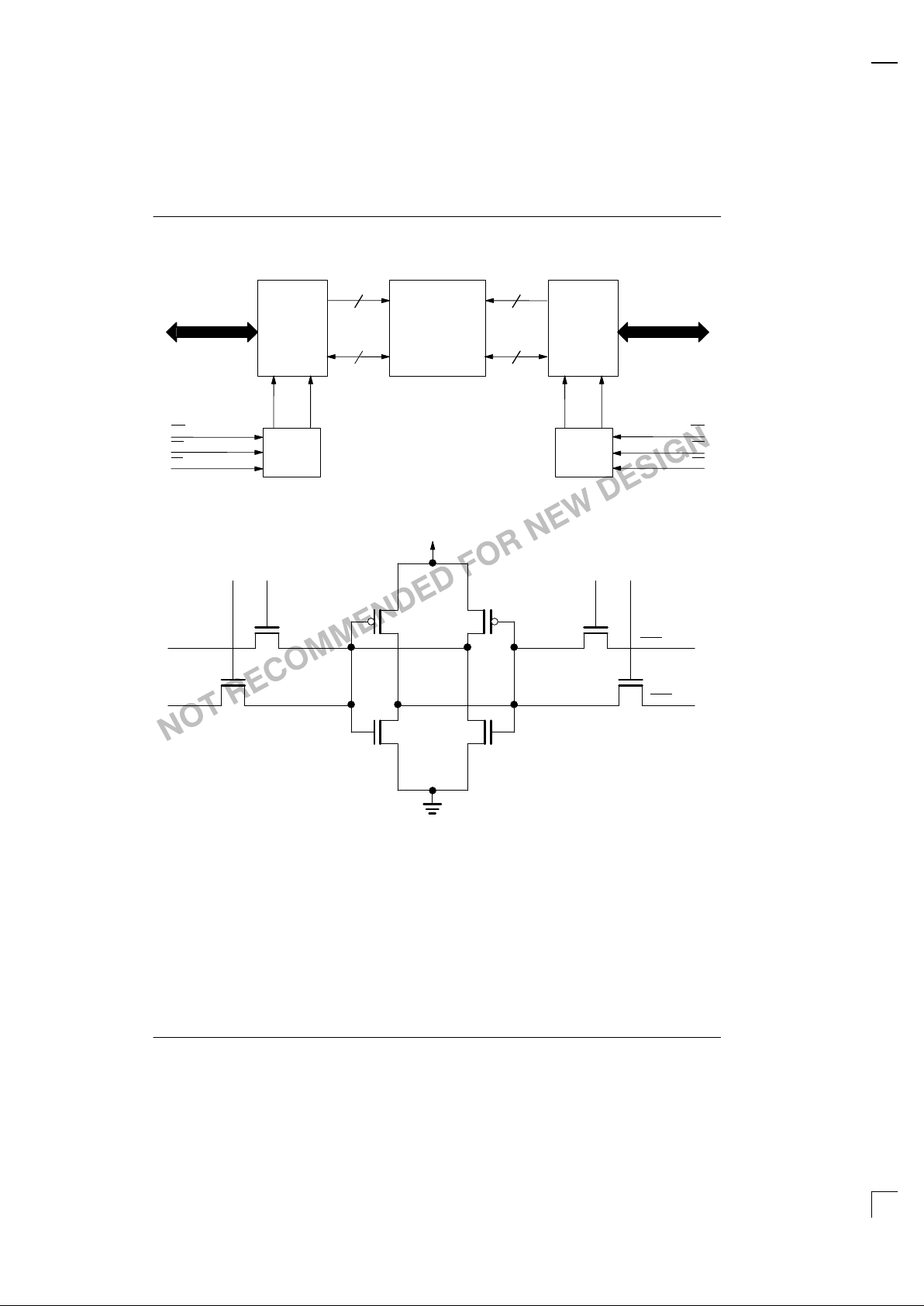
The main elements of the dual port RAM are shown in
Figure 1.
A read cycle to either port begins by placing an address
on the multiplexed bus pins AD0 – AD7. The port enable
control (CE
) is then transitioned low. This control signal
causes address to be latched internally. Addresses can
be removed from the bus provided address hold time is
met. Next, the output enable control (OE
) is transitioned
low, which begins the data access portion of the read
cycle. With both CE and OE active low, data will appear
valid after the output enable access time t
OEA
. Data will
remain valid as long as both port enable and output enable remains low. A read cycle is terminated with the
first occurring rising edge of either CE or OE. The address/data bus will return to a high impedance state after time t
CEZ
or t
OEZ
as referenced to the first occurring
rising edge. WE must remain high during read cycles.
OPERATION – WRITE CYCLE
A write cycle to either port begins by placing an address
on the multiplexed bus pins AD0 – AD7. The port enable
control (CE
) is then transitioned low. This control signal
causes address to be latched internally. As with a read
cycle, the address can be removed from the bus provided address hold time is met. Next the write enable
control signal (WE
) is transitioned low which begins the
write data portion of the write cycle. With both CE and
WE
active low the data to be written to the selected
memory location is placed on the multiplexed bus. Provided that data setup (tDS) and data hold (tDH) times are
met, data is written into the memory and the write cycle
is terminated on the first occurring rising edge of either
CE
or WE. Data can be removed from the bus as soon
as the write cycle is terminated. OE
must remain high
during write cycles.
ARBITRATION
The DS1609 dual port RAM has a special cell design
that allows for simultaneous accesses from two ports
(see Figure 2). Because of this cell design, no arbitration is required for read cycles occurring at the same instant. However, an argument for arbitration can be
made for reading and writing the cell at the exact same
instant or for writing from both ports at the same instant.
A simple way to assure that read/write conflicts don’t occur is to perform redundant read cycles. Write/write arbitration needs can be avoided by assigning groups of
addresses for write operation to one port only. Groups
of data can be assigned check sum bytes which would
guarantee correct transmission. A software arbitration
system using a “mail box” to pass status information can
also be employed. Each port could be assigned a
unique byte for writing status information which the other port would read. The status information could tell the
reading port if any activity is in progress and indicate
when activity is going to occur.

DS1609
020499 3/7
BLOCK DIAGRAM: DUAL PORT RAM Figure 1
PORT A
MUX ADDRESS/DATA
ADDRESS/
DATA MUX
LATCH
DECODE
256 BYTE DUAL
PORT MEMORY
MATRIX
8 ADDRESS
8 DATA
8 ADDRESS
8 DATA
PORT B
ADDRESS/
DATA MUX
LATCH
DECODE
MUX ADDRESS/DATA
WE
OE
CE
CONTROL
LOGIC
CONTROL
LOGIC
WE
OE
CE
DUAL PORT MEMORY CELL Figure 2
V
CC
DATA–PORT A
DATA
–PORT B
DATA–PORT A
DATA–PORT B
 Loading...