Dallas Semiconductor DS1397, DS1395 Datasheet

DS1395/DS1397
DS1395/DS1397
RAMified Real Time Clock
FEATURES
• Ideal for EISA bus PCs
• Functionally compatible with MC146818 in 32 KHz
mode
• Totally nonvolatile with over 10 years of operation in
the absence of power
• Self-contained subsystem includes lithium, quartz,
and support circuitry
• Counts seconds, minutes, hours, day of the week,
date, month, and year with leap year compensation
• Binary or BCD representations of time, calendar, and
alarm
• 12- or 24-hour clock with AM and PM in 12-hour mode
• Daylight Savings Time option
• Interfaced with software as 64 register/RAM locations
plus 4K x 8 of static RAM
– 14 bytes of clock and control registers
– 50 bytes of general and control registers
– Separate 4K x 8 nonvolatile SRAM
• Programmable square wave output signal
• Bus-compatible interrupt signals (IRQ)
• Three interrupts are separately software-maskable
and testable:
– Time-of-day alarm once/second to once/day
– Periodic rates from 122 µs to 500 ms
– End-of-clock update cycle
• 28-pin JEDEC footprint
• Available as chip (DS1395/DS1395S) or stand alone
module with embedded lithium battery and crystal
(DS1397)
ORDERING INFORMATION
DS1395 RTC Chip; 28–pin DIP
DS1395S RTC Chip; 28–pin SOIC
DS1397 RTC Module; 28–pin DIP
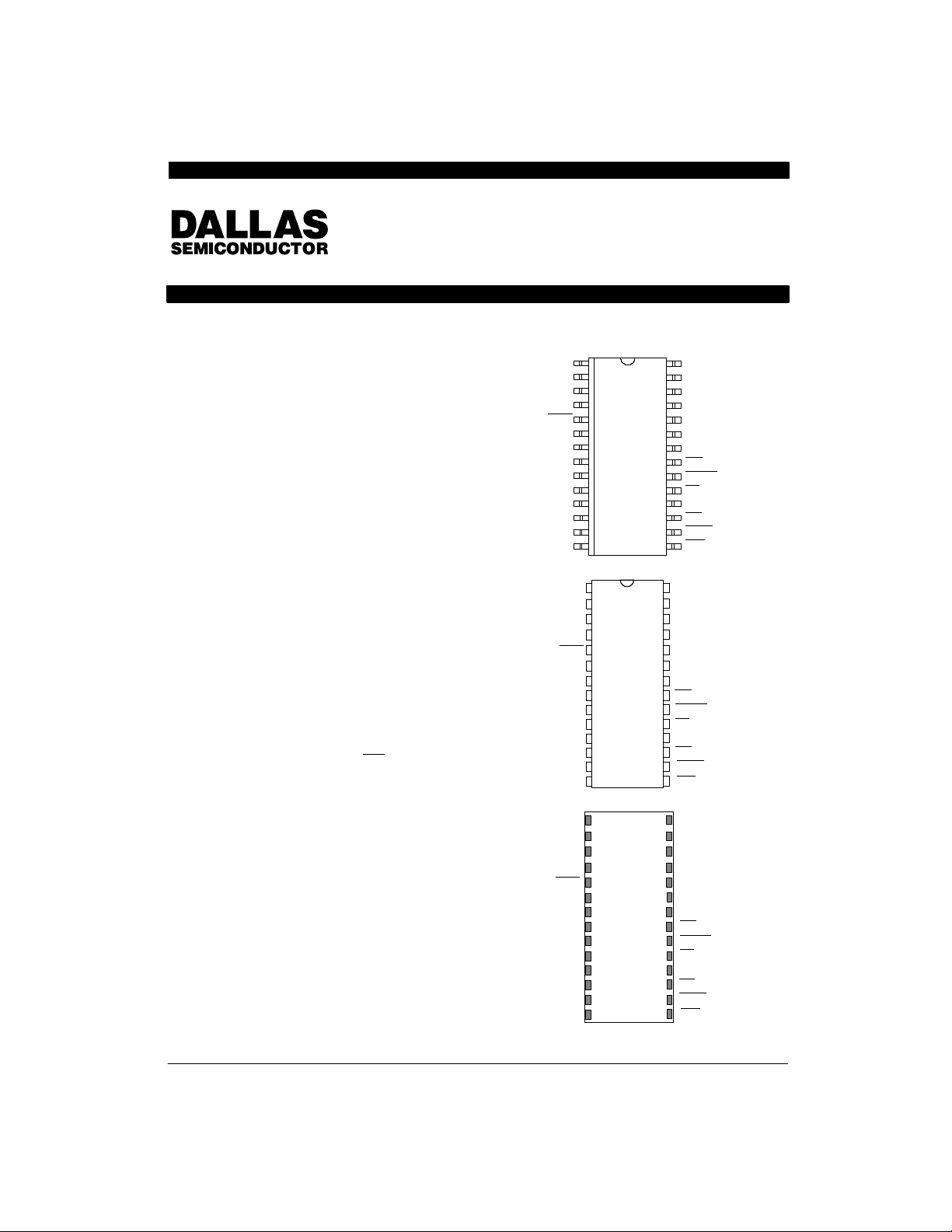
PIN ASSIGNMENT
1
A0
2
A1
3
X2
4
X1
STBY
DS1397 28-Pin Encapsulated Package (720 mil)
5
D0
6
7
D1
8
D2
9
D3
D4
10
D5
11
D6
12
D7
13
V
14
SS
DS1395S 28-Pin SOIC (330 mil)
1
A0
2
A1
3
X2
4
X1
5
STBY
6
D0
7
D1
8
D2
9
D3
10
D4
11
D5
12
D6
13
D7
V
14
SS
DS1395 28-Pin DIP (600 mil)
1
2
A1
3
NC
4
NC
5
STBY
D0
6
D1
7
D2
8
D3
9
D4
10
D5
11
D6
12
D7
13
V
14 15
SS
A2
28
27
A3
V
26
DD
SQW
25
A4
24
A5
23
V
22
BAT
IRQ
21
RESET
20
RD
19
B
18
GND
WR
17
XRAM
16
RTC
15
A2
28
A3
27
V
26
DD
SQW
25
A4
24
A5
23
V
22
BAT
IRQ
21
RESET
20
RD
19
B
18
GND
WR
17
XRAM
16
15
RTC
A2
28A0
A3
27
V
26
DD
SQW
25
A4
24
A5
23
NC
22
IRQ
21
RESET
20
RD
19
NC
18
WR
17
XRAM
16
RTC
Copyright 1995 by Dallas Semiconductor Corporation.
All Rights Reserved. For important information regarding
patents and other intellectual property rights, please refer to
Dallas Semiconductor databooks.
020794 1/19

DS1395/DS1397
PIN DESCRIPTIONS
V
VSS – Bus operational power is supplied to the part
DD,
via these pins. The voltage level present on these pins
should be monitored to transition between operational
power and battery power.
D0-D7 – Data Bus (bidirectional): Data is written into
the device from the data bus if either XRAM
asserted during a write cycle at the rising edge of a WR
pulse. Data is read from the device and driven onto the
data bus if either XRAM or RTC is asserted during a
read cycle when the RD signal is low.
A0-A5 – Address Bus (input): Various internal registers of the device are selected by these lines. When
RTC
is asserted, A0 selects between the indirect address register and RTC data register . When the XRAM
is asserted, A0-A5 addresses a 32–byte page of RAM.
When A5 is high, the RAM page register is accessible.
When A5 is low, A0-A4 address the 32-byte page of
RAM.
RD
- Read Strobe (input): Data is read from the se-
lected register and driven onto the data bus by the device when this line is low and either RTC or XRAM is asserted.
WR
- Write Strobe (input): Data is written into the de-
vice from the data bus on the rising edge after a low
pulse on this line when the device has been selected by
either the XRAM or RTC signals.
or RTC is
cessible. Registers are selected by the A0 line. Data is
driven onto the data bus when RD
is low. Data is received from the bus when WR is pulsed low and then
high.
SQW - Square Wave (output): Frequency selectable
output. Frequency is selected by setting register A bits
RS0-RS3. See T able 2 for frequencies that can be selected.
XRAM
- Extended RAM Select (input): When this sig-
nal is asserted low, the extended RAM bytes are accessible. The XRAM page register is selected when the A5
address line is high. A 32-byte page of RAM is accessible when A5 is low. A0-A4 select the bytes within the
page of RAM pointed to by the page register. Data is
driven onto the data bus when RD
is low. Data is received from the bus when WR is pulsed low and then
high.
IRQ
- Interrupt Request (output): The IRQ signal is an
active low, open drain output that is used as a processor
interrupt request. The IRQ
output follows the state of
the IRQF bit (bit 7) in status register C. IRQ can be asserted by the alarm, update ended, or periodic interrupt
functions depending on the configuration of register B.
RESET
- Reset (input): The reset signal is used to ini-
tialize certain registers to allow proper operation of the
RTC module. When RESET
is low, the following oc-
curs.
STBY
- Standby (input): Accesses to the device are
inhibited and outputs are tri-stated to a high impedance
state when this signal is asserted low. All data in RAM of
the device is preserved. The real time clock continues
to keep time.
If a read or write cycle is in progress when the STBY
signal is asserted low, the internal cycle will be terminated
when either the external cycle completes or when the internal chip enable condition (V
is 4.25 volts, typical) is
DD
negated, whichever occurs first.
RTC
- Real Time Clock Select (input): When this sig-
nal is asserted low, the real time clock registers are ac-
020794 2/19
1. The following register bits are cleared:
a. Periodic interrupt (PIE)
b. Alarm interrupt enable (AIE)
c. Update ended interrupt (UF)
d. Interrupt request flag (IRQF)
e. Periodic interrupt flag (PF)
f. Alarm interrupt flag (AF)
g. Square wave output enable (SQWE)
h. Update ended interrupt enable (UIE)
2. The IRQ
pin is in the high impedance state.
3. The RTC is not processor accessible.

DS1395/DS1397
ADDITIONAL PIN DESCRIPTION
(FOR DS1395, DS1395S)
X1, X2 – Connections for a standard 32.768 KHz quartz
crystal, Daiwa part number DT-26S or equivalent. The
internal oscillator circuitry is designed for operation with
a crystal having a specified load capacitance (C
L
) of
6 pF . The crystal is connected directly to the X1 and X2
pins. There is no need for external capacitors or resistors. Note: X1 and X2 are very high impedance nodes.
It is recommended that they and the crystal be guard–
ringed with ground and that high frequency signals be
kept away from the crystal area. For more information
on crystal selection and crystal layout considerations,
please consult Application Note 58, “Crystal Considerations with Dallas Real Time Clocks”.
V
– Battery input for any standard +3 volt lithium cell
BAT
or other energy source. Battery voltage must be held
between 2.5 and 3.5 volts for proper operation. The
nominal write protect trip point voltage at which access
to the real time clock and user RAM is denied is set by
the internal circuitry as 1.26 x V
1 µA at 25oC and 3.0V on V
. A maximum load of
BAT
in the absence of power
BAT
should be used to size the external energy source.
The battery should be connected directly to the V
BAT
pin. A diode must not be placed in series with the battery
to the V
pin. Furthermore, a diode is not necessary
BAT
because reverse charging current protection circuitry is
provided internal to the device and has passed the
requirements of Underwriters Laboratories for UL listing.
B
– Battery ground: This pin or pin 14 can be used
GND
for the battery ground return.
OPERATION
Power-Down/Power-Up: The real time clock will con-
tinue to operate and all of the RAM, time, and calendar
and alarm memory locations will remain non-volatile regardless of the voltage level of VDD. When the voltage
level applied to the V
(typical), the module becomes accessible after 200 ms
provided that the oscillator and countdown chain have
been programmed to be running. This time period allows the module to stabilize after power is applied.
input is greater than 4.25 volts
DD
When V
falls below the CE
DD
(4.25 volts typical), the
THR
chip select inputs RTC and XRAM are forced to an inactive state regardless of the state of the pin signals. This
puts the module into a write protected mode in which all
inputs are ignored and all outputs are in a high impedance state. When V
falls below 3.2 volts (typical), the
DD
module is switched over to an internal power source in
the case of the DS1397, or to an external battery connected to the V
and BGND pins in the case of the
BAT
DS1395 and DS1395S, so that power is not interrupted
to timekeeping and nonvolatile RAM functions.
Address Map: The registers of the device appear in two
distinct address ranges. One set of registers is active
when RTC
is asserted low and represents the real time
clock. The second set of registers is active when XRAM
is asserted low and represents the extended RAM.
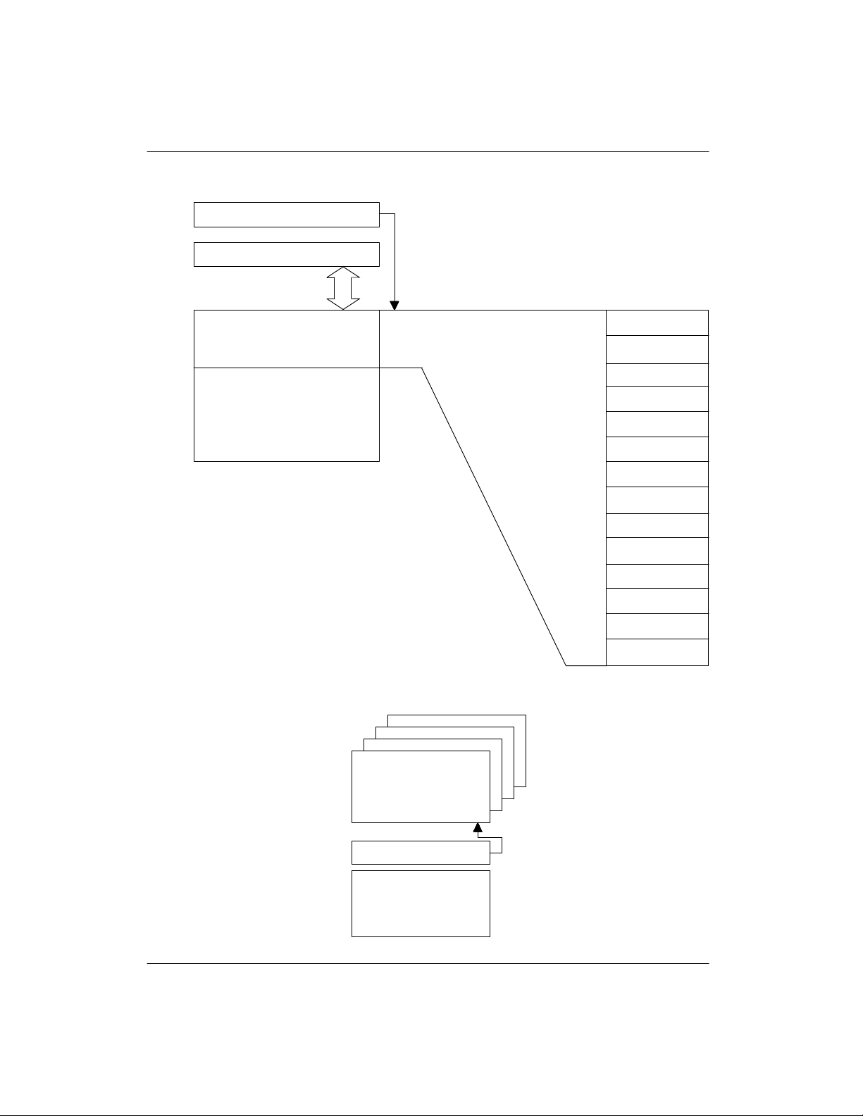
RTC Address Map: The address map of the RTC module is shown in Figure 2. The address map consists of
50 bytes of general purpose RAM, 10 bytes of RTC/calendar information, and 4 bytes of status and control information. All 64 bytes can be accessed as read/write
registers except for the following:
1. Registers C and D are Read Only (status informa-
tion)
2. Bit 7 of register A is Read Only
3. Bit 7 of the ”Seconds” byte (00) is Read Only
The first byte of the real time clock address map is the
RTC indirect address register, accessible when A0 is
low. The second byte is the RTC data register , accessible when A0 is high. The function of the RTC indirect address register is to point to one of the 64 RTC registers
that are indirectly accessible through the RTC data register.
Extended RAM Address Map: The first 32 bytes of the
extended RAM represent one of 128 pages of general
purpose nonvolatile memory . These 32 bytes on a page
are addressed by A0 through A4 when A5 is low. When
A5 is high, the XRAM page register is accessible. The
value in the XRAM page register points to one of 128
pages of nonvolatile memory available. The address of
the XRAM page register is dependent only on A5 being
high; thus, there are 31 aliases of this register in I/0
spaces. (See Figure 3.)
020794 3/19

DS1395/DS1397
TIME, CALENDAR AND ALARM LOCATIONS
The time and calendar information is obtained by reading the appropriate register bytes shown in T able 1. The
time, calendar, and alarm are set or initialized by writing
the appropriate register bytes. The contents of the time,
calendar, and alarm registers can be either Binary or
Binary-Coded Decimal (BCD) format. Table 1 shows
the binary and BCD formats of the twelve time, calendar,
and alarm locations.
Before writing the internal time, calendar, and alarm registers, the SET bit in Register B should be written to a
logic one to prevent updates from occurring while access is being attempted. Also at this time, the data format (binary or BCD), should be set via the data mode bit
(DM) of Register B. All time, calendar, and alarm registers must use the same data mode. The set bit in Register B should be cleared after the data mode bit has been
written to allow the real-time clock to update the time
and calendar bytes.
Once initialized, the real-time clock makes all updates in
the selected mode. The data mode cannot be changed
without reinitializing the ten data bytes. The 24/12 bit
cannot be changed without reinitializing the hour locations. When the 12-hour format is selected, the high or-
der bit of the hours byte represents PM when it is a logic
one. The time, calendar, and alarm bytes are always accessible because they are double buffered. Once per
second the ten bytes are advanced by one second and
checked for an alarm condition. If a read of the time and
calendar data occurs during an update, a problem exists
where seconds, minutes, hours, etc. may not correlate.
The probability of reading incorrect time and calendar
data is low. Several methods of avoiding any possible
incorrect time and calendar reads are covered later in
this text.
The three alarm bytes can be used in two ways. First,
when the alarm time is written in the appropriate hours,
minutes, and seconds alarm locations, the alarm interrupt is initiated at the specified time each day if the alarm
enable bit is high . The second method is to insert a
“don’t care” state in one or more of the three alarm bytes.
The “don’t care” code is any hexadecimal value from C0
to FF . The two most significant bits of each byte set the
“don’t care” condition when at logic 1. An alarm will be
generated each hour when the “don’t care” bits are set in
the hours byte. Similarly, an alarm is generated every
minute with “don’t care” codes in the hours and minute
alarm bytes. The “don’t care” codes in all three alarm
bytes create an interrupt every second.
020794 4/19

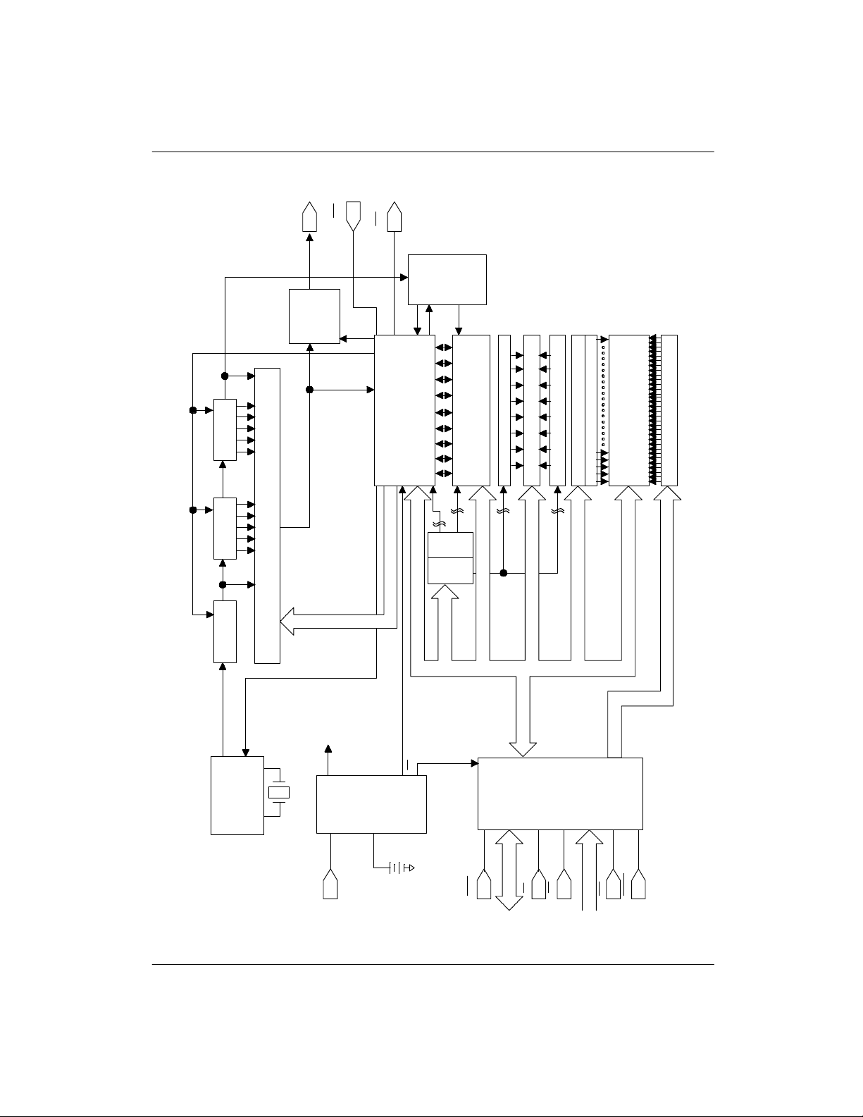
DS139X BLOCK DIAGRAM Figure 1
SQ WAVE
OUT
RST
2
÷
SQW
IRQ
CLOCK
UPDATE
CALENDAR
DS1395/DS1397
RST
64
÷
RST
64
÷
RST
8
÷
KHz
32.768
ON/OFF
OSC
PERIODIC INTR/SQ WAVE SELECTOR
RS0–RS3
PP
V
POWER
SWITCHING
REFERENCE
A,B,C,D
REGISTERS
PCK
CE
CLOCK CALENDAR
10
4
DECODER
REGISTER
INDEX
REGISTERS
AND ALARM
50 BYTES USER RAM
COLUMN DECODER 1 OF 8
3
DATA/CONTROL
EXTENDED RAM
ROW DECODER, 1 OF 8
COLUMN DECODER, 1 OF 16
EXTENDED RAM PAGE REGISTER
3
A0–A3
BUS
INTERFACE
4096 BYTES
ROW DECODER, 1 OF 256
A4–A11
BAT
V
DD
V
STBY
D0–D7
RD
WR
A0–A5
RTC
XRAM
020794 5/19

DS1395/DS1397
REAL TIME CLOCK RAM MAP Figure 2
RTC
RTC +1
INDIRECT
ADDRESS
00
INDIRECT ADDRESS REGISTER
RTC DATA REGISTER
13
14
63
14–BYTES
RTC
50–BYTES
USER RAM
14– BYTES
REAL TIME CLOCK
00
0D
0E
3F
00
01
02
03
04
05
06
07
08
09
0A
0B
SECONDS
SECONDS ALARM
MINUTES
MINUTES ALARM
HOURS
HOURS ALARM
DAY OF WEEK
DAY OF MONTH
MONTH
YEAR
REGISTER A
REGISTER B
EXTENDED RAM ADDRESS MAP Figure 3
XRAM
THRU
XRAM + 1F
XRAM + 20
XRAM + 21
THRU
XRAM + 3F
020794 6/19
EXTENDED RAM
XRAM PAGE REGISTER
PAGE REGISTER
128 PAGES
OF 32–BYTES
ALIASES OF
02
01
PAGE 00
PAGE 7F
0C
REGISTER C
0D
REGISTER D
 Loading...