Dallas Semiconductor DS1336SN, DS1336S, DS1336N, DS1336 Datasheet

1 of 6 050699
FEATURES
§ Provides power switching of up to 1.5 amps at
voltages between 3.0 and 5.0 volts
§ Five separate power switches
§ Selectable battery switches for use with
§ battery-backed systems
§ Very low on impedance of 0.7O
§ Battery backup current of 4 mA
§ Diode-isolated battery path
§ Available in 16-pin DIP or 16-pin SOIC
surface
§ mount package
§ Low voltage drop battery path
§ Connects directly to a variety of Dallas
Semiconductor devices, adding increased
switching capability for large battery backup
current applications
PIN ASSIGNMENT
PIN DESCRIPTION
VCC/IN1 - +5V Input and Input 1
IN2 - IN5 - Inputs 2 - 5
OUT1 - 5 - Outputs 1 - 5
V
BATIN
- External Battery Input
V
BAT01
- Diode Protected Battery Output
V
BAT02
- Low Voltage Drop Battery
Output
PF,
PF
- Power-fail Inputs
GND - Ground
DESCRIPTION
The DS1336 Afterburner Chip is designed to provide power switching between a primary power supply
(VCC) and a backup battery power supply (V
BAT
). Five V
CC
and two battery paths are provided which can
be used individually or in parallel to supply uninterrupted power in applications such as SRAM networks.
When used with one of the Dallas power monitoring devices listed in Table 1, the DS1336 allows a load
to be switched from its main power supply VCC to a battery backup supply when VCC falls out of
tolerance. A user may selectively tie together any combination of the output pins to provide the desired
high current supply, providing up to 300 mA per OUT pin or a maximum of 1.5A. Depending upon the
user’s backup supply load requirements, either of the V
BAT
outputs may be tied to the OUT pins to supply
DS1336
Afterburner Chip
www.dalsemi.com
16-Pin DIP (300-mil)
See Mach. Drawings
Section
16-Pin DIP SOIC (300-mil)
See Mach. Drawings
Section
OUT5
PF
IN5
IN2
IN4
VBATIN
VBAT02
OUT4
116151413
12111092345678V/IN1PFGND
OUT1
OUT2
OUT3
VBAT01
IN3
OUT5
PF
IN5
IN2
IN4
VBATIN
VBAT02
OUT4
116151413
121110923456
78V
/IN1
PF
GND
OUT1
OUT2
VBAT01
IN3

DS1336
2 of 6
current when VCC is out of tolerance. The DS1336 switches back to the higher current VCC from battery
current when PF and PF become inactive.
OPERATION
The required PF or PF input which controls the switching between the main VCC and backup battery can
be supplied by any of the devices listed in Table 1. All of the devices provide the DS1336 with a PF or
PF
signal, switching between a main supply VCC and backup supply V
BAT
when VCC falls out of
tolerance. For applications requiring switching from the VCC supply inputs to V
BAT
, the required PF or
PF
input to the DS1336 can be provided by the DS1236, DS1239, DS5001, or DS5340. For applications
requiring switching from the VCC inputs to the V
BAT
input when VCC begins falling out of tolerance, any
of the Dallas Semiconductor devices listed in Table 1 can provide the DS1336 with the required
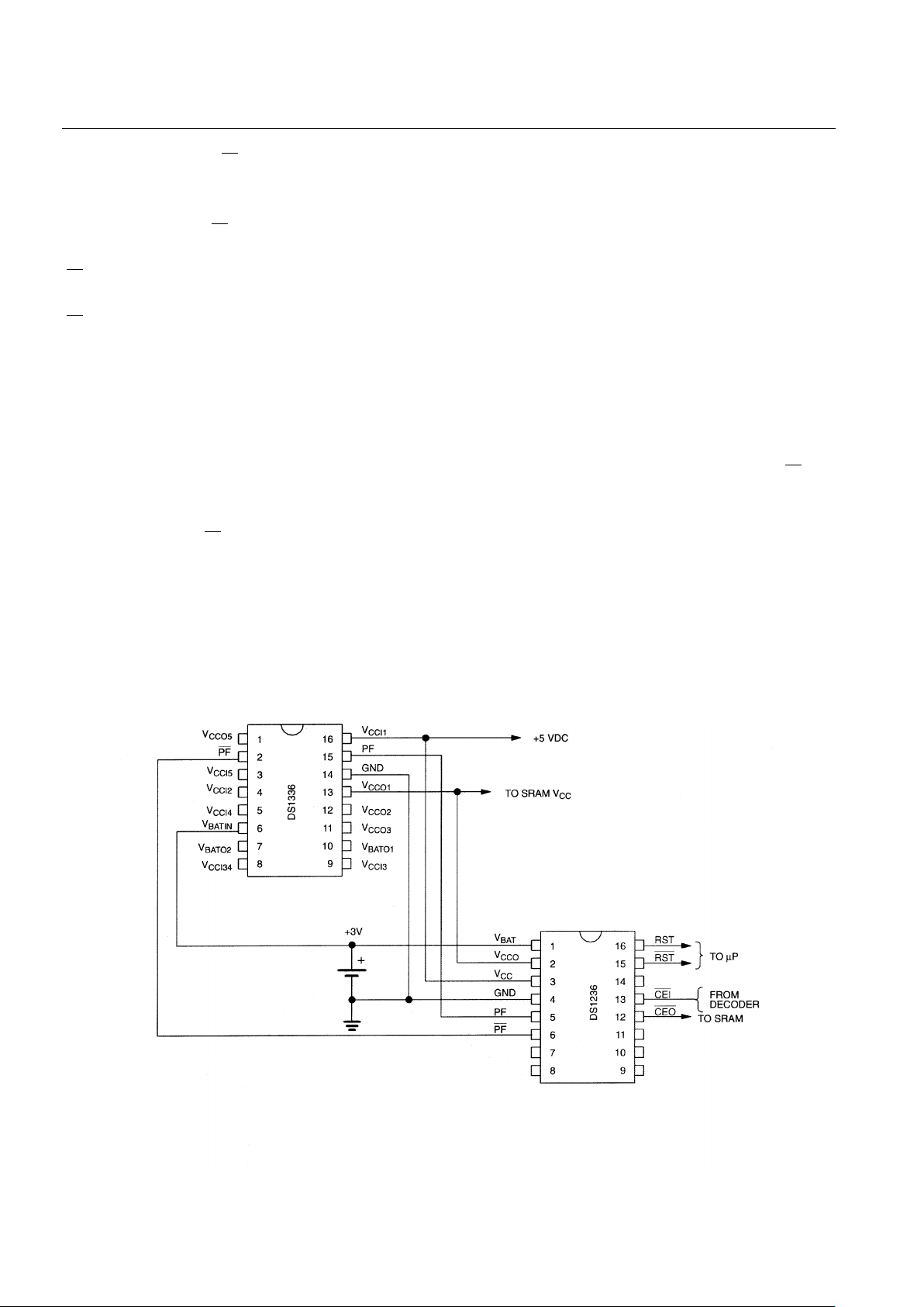
switching input. A typical application is shown in Figure 1. For applications where switching between
VCC and V
BAT
must occur at a voltage level such that VCC is still greater than V
BAT
, the OUT5 pin is
recommended as it provides a diode path which will provide for a gradual transition between VCC and
V
BAT
. OUT5 can be tied to the other OUTPUT pins to provide a gradual transition for all five current
paths. In applications where tri-state switching is desired, OUT5 should be omitted. Only the PF/PF pin
is required for switching. In cases where the PF input will not be used, it should be connected to GND.
When either PF or PF is active, either of the V
BAT0X
outputs is available, although they should not be tied
together (Figure 2, “DS1336 Block Diagram”). V
BAT01
is recommended for sensitive applications such as
providing backup current to timekeepers, because its diode isolated path provides for increased
protection. V
BAT02
is not recommended for applications where it would be tied to an OUTPUT pin
supplying a voltage greater than that of the backup battery because V
BAT02
is not a diode isolated current
path.
TYPICAL APPLICATION Figure 1
 Loading...