Dallas Semiconductor DS12885TN, DS12885T-T-R, DS12885T, DS12885S, DS12885QN Datasheet
...
1 of 6 072902
Note:
Some revisions
of this device may incorporate deviations from published specifications known as errata. Multiple revisions of any device
may be simultaneously available through various sales channels. For information about device errata, click here: http://www.maxim -ic.com/errata.
FEATURES
§ Drop-in replacement for IBM AT computer
clock/calendar
§ Pin configuration closely matches
MC146818B and DS1285
§ Counts seconds, minutes, hours, days, day of
the week, date, month, and year with leapyear compensation valid up to 2100
§ Binary or BCD representation of time,
calendar, and alarm
§ 12-hour or 24-hour clock with AM and PM in
12-hour mode
§ Daylight Savings Time option
§ Selectable between Motorola and Intel bus
timing
§ Multiplex bus for pin efficiency
§ Interfaced with software as 128 RAM
locations
§ 14 bytes of clock and control registers
§ 114 bytes of general purpose RAM
§ Programmable square-wave output signal
bus-compatible interrupt signals (IRQ )
§ Three interrupts are separately softwaremaskable and testable
§ Time-of -day alarm once/second to once/day
§ Periodic rates from 122µs to 500ms
§ End-of -clock update cycle
§ Optional 28-pin PLCC surface mount package
or 32-pin TQFP
§ Optional industrial temperature range
available
§ Underwriters Laboratory (UL) recognized
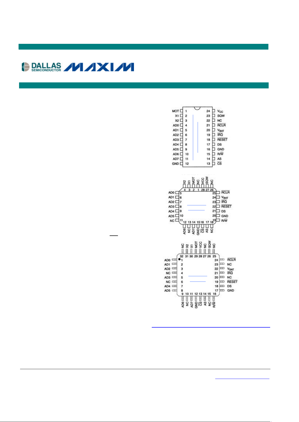
PIN ASSIGNMENT (Top View)
Package Dimension Information
http://www.maxim-ic.com/TechSupport/DallasPackInfo.htm
DS12885/DS12885Q/DS12885T
Real-
Time Clock
www
.
maxim
-ic.com
www.maxim
-
ic.com
DS12885Q
28 PLCC
DS12885T
32 TQFP
DS12885, 24 DIP
DS12885S, 24 SO 300mil

DS12885/DS12885Q/DS12885T
2 of 4
DESCRIPTION
The DS12885 real-time clock plus RAM is designed to be a direct replacement for the DS1285. The
DS12885 is identical in form, fit, and function to the DS1285, and has an additional 64 bytes of general
purpose RAM. Access to this additional RAM space is determined by the logic level presented on AD6
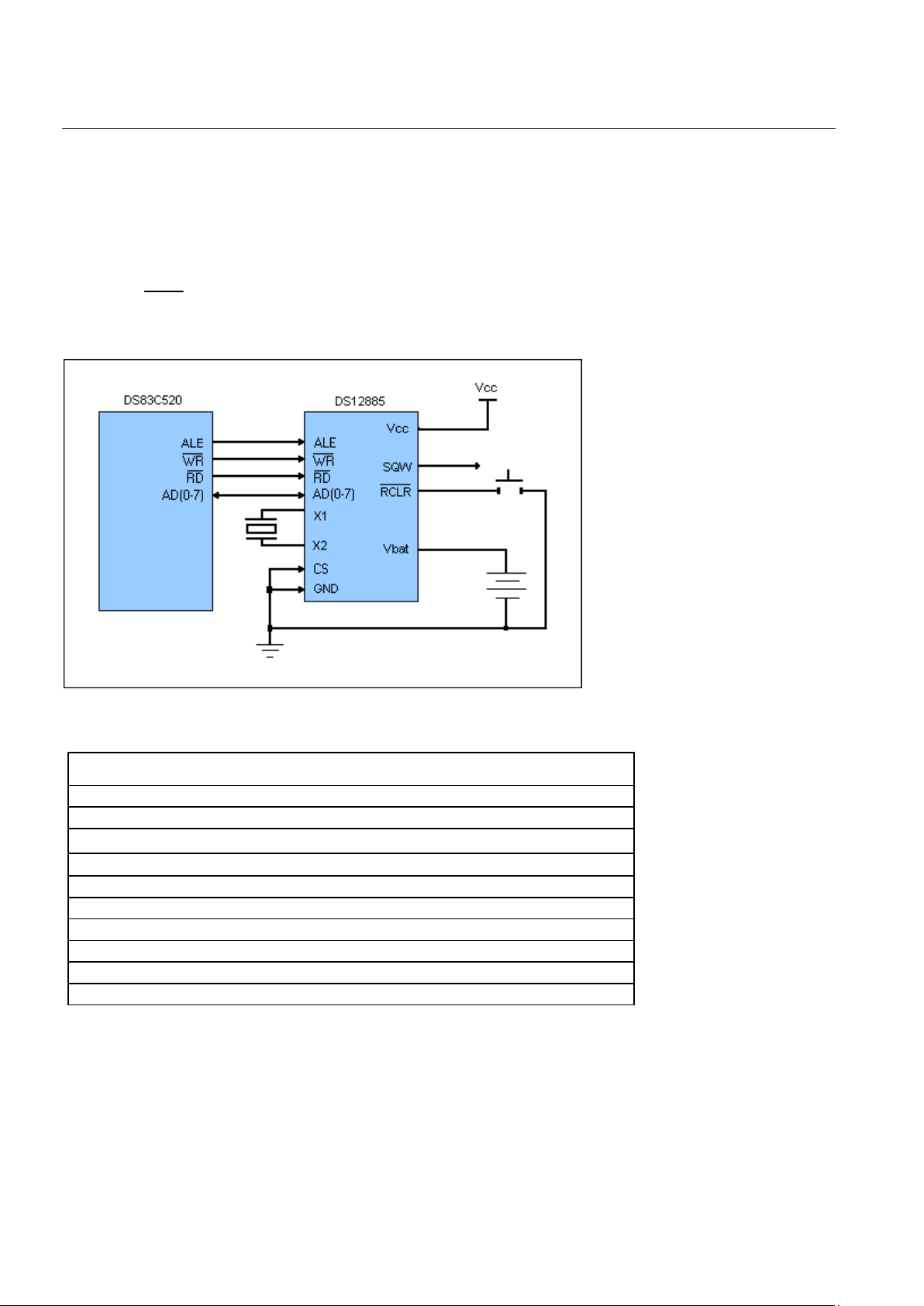
during the address portion of an access cycle. An external crystal and battery are the only components
required to maintain time-of-day and memory status in the absence of power. For a complete description
of operating conditions, electrical characteristics, bus timing, and pin descriptions other than X1, X2,
V
BAT
, and RCLR , see the DS12887 data sheet.
TYPICAL OPERATING CIRCUIT
ORDERING INFORMATION
PART PIN-PACKAGE TEMP RANGE
DS12885 24 DIP 0°C to +70°C
DS12885N 24 DIP -40°C to +85°C
DS12885S
24 SO 0°C to +70°C
DS12885N 24 SO -40°C to +85°C
DS12885Q 28 PLCC 0°C to +70°C
DS12885QN 28 PLCC -40°C to +85°C
DS12885Q/T&R 28 PLCC/Tape and Reel 0°C to +70°C
DS12885T 32 TQFP 0°C to +70°C
DS12885TN 32 TQFP -40°C to +85°C
DS12885T/T&R 32 TQFP/Tape and Reel 0°C to +70°C
 Loading...