Dallas Semiconductor DS1267S-010, DS1267E-100-T-R, DS1267E-100, DS1267E-050-T-R, DS1267E-050 Datasheet
...
1 of 12 102199
VB
NC
H1
L1
W1
RST
CLK
GND
16
15
14
13
12
11
10
9
1
2
3
4
5
6
7
8
V
CC
NC
S
OUT
W0
H0
L0
C
OUT
DQ
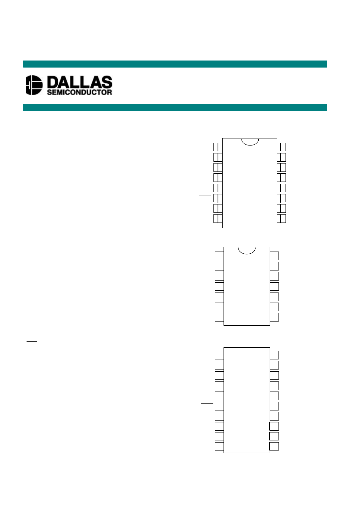
16-Pin SOIC (300-mil)
See Mech. Drawings Section
FEATURES
§ Ultra-low power consumption, quiet,
pumpless design
§ Two digitally controlled, 256-position
potentiometers
§ Serial port provides means for setting and
reading both potentiometers
§ Resistors can be connected in series to
provide increased total resistance
§ 14-pin DIP, 16-pin SOIC, 20-pin TSSOP
packages
§ Resistive elements are temperature
compensated to ±0.3 LSB relative linearity
§ Standard resistance values:
– DS1267-10 ~ 10 kΩ
– DS1267-50 ~ 50 kΩ
– DS1267-100 ~ 100 kΩ
§ Operating Temperature Range:
– Industrial: -40°C to +85°C
PIN ASSIGNMENT
PIN DESCRIPTIONS
L0, L1 - Low End of Resistor
H0, H1 - High End of Resistor
W0, W1 - Wiper Terminal of Resistor
V
B
- Substrate Bias Voltage
S
OUT
- Stacked Configuration Output
RST - Serial Port Reset Input
DQ - Serial Port Data Input
CLK - Serial Port Clock Input
C
OUT
- Cascade Port Output
V
CC
- +5 Volt Supply
GND - Ground
NC - No Internal Connection
14-Pin DIP (300-mil)
See Mech. Drawings Section
VB
H1
L1
W1
RST
CLK
GND
14
13
12
1110981
2
3
4567V
CC
S
OUT
W0
H0L0C
OUT
DQ
DS1267
Dual Digital Potentiometer Chip
www.dalsemi.com
20-Pin TSSOP (173-mil)
VB
NC
H1
L1
W1
RST
CLK
20
19
18
17
16
15
14
1
2
3
4
5
6
7
V
CC
NC
NC
S
OUT
W0
H0L08910131211C
OUT
NCNCNC
GND
DQ

DS1267
2 of 12 102199
DESCRIPTION
The DS1267 Dual Digital Potentiometer Chip consists of two digitally controlled, solid-state
potentiometers. Each potentiometer is composed of 256 resistive sections. Between each resistive section
and both ends of the potentiometer are tap points which are accessible to the wiper. The position of the
wiper on the resistive array is set by an 8-bit value that controls which tap point is connected to the wiper
output. Communication and control of the device are accomplished via a 3-wire serial port interface.
This interface allows the device wiper position to be read or written.
Both potentiometers can be connected in series (or stacked) for an increased total resistance with the
same resolution. For multiple-device, single-processor environments, the DS1267 can be cascaded or
daisy-chained. This feature provides for control of multiple devices over a single 3-wire bus.
The DS1267 is offered in three standard resistance values which include 10, 50, and 100-kohm versions.
Available packages for the device include a 14-pin DIP, 16-pin SOIC, and 20-pin TSSOP.
OPERATION
The DS1267 contains two 256-position potentiometers whose wiper positions are set by an 8-bit value.
These two 8-bit values are written to a 17-bit I/O shift register that is used to store the two wiper positions
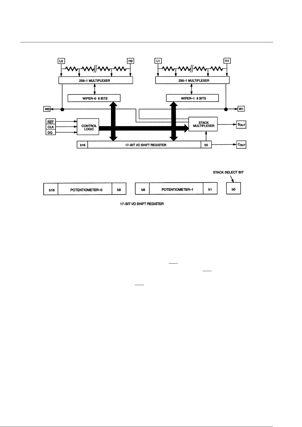
and the stack select bit when the device is powered. A block diagram of the DS1267 is presented in
Figure 1.
Communication and control of the DS1267 are accomplished through a 3-wire serial port interface that
drives an internal control logic unit. The 3-wire serial interface consists of the three input signals: RST ,
CLK, and DQ.
The RST control signal is used to enable the 3-wire serial port operation of the device. The chip is
selected when RST is high; RST must be high to begin any communication to the DS1267. The CLK
signal input is used to provide timing synchronization for data input and output. The DQ signal line is
used to transmit potentiometer wiper settings and the stack select bit configuration to the 17-bit I/O shift
register of the DS1267.
Figure 9(a) presents the 3-wire serial port protocol. As shown, the 3-wire port is inactive when the RST
signal input is low. Communication with the DS1267 requires the transition of the RST input from a low
state to a high state. Once the 3-wire port has been activated, data is entered into the part on the low to
high transition of the CLK signal inputs. Three-wire serial timing requirements are provided in the timing
diagrams of Figure 9(b)-(c).
Data written to the DS1267 over the 3-wire serial interface is stored in the 17-bit I/O shift register (see
Figure 2). The 17-bit I/O shift register contains both 8-bit potentiometer wiper position values and the
stack select bit. The composition of the I/O shift register is presented in Figure 2. Bit 0 of the I/O shift
register contains the stack select bit, which will be discussed in the section entitled "Stacked
Configuration." Bits 1 through 8 of the I/O shift register contain the potentiometer-1 wiper position value.
Bit 1 contains the MSB of the wiper setting for potentiometer-1 and bit 8 the LSB for the wiper setting.
Bits 9 through 16 of the I/O shift register contain the value of the potentiometer-0 wiper position, with the
MSB for the wiper position occupying bit 9 and the LSB bit 16.

DS1267
3 of 12 102199
DS1267 BLOCK DIAGRAM Figure 1
I/O SHIFT REGISTER Figure 2
Transmission of data always begins with the stack select bit followed by the potentiometer-1 wiper
position value and lastly the potentiometer-0 wiper position value.
When wiper position data is to be written to the DS1267, 17 bits (or some integer multiple) of data should
always be transmitted. Transactions which do not send a complete 17-bits (or multiple) will leave the
register incomplete and possibly an error in the desired wiper positions.
After a communication transaction has been completed, the RST signal input should be taken to a low
state to prevent any inadvertent changes to the device shift register. Once RST has reached a low state,
the contents of the I/O shift register are loaded into the respective multiplexers for setting wiper position.
A new wiper position will only engage after a RST transition to the inactive state. On device power-up
the DS1267 wiper positions will be set at 50% of the total resistance or binary value 1000 0000.

DS1267
4 of 12 102199
STACKED CONFIGURATION
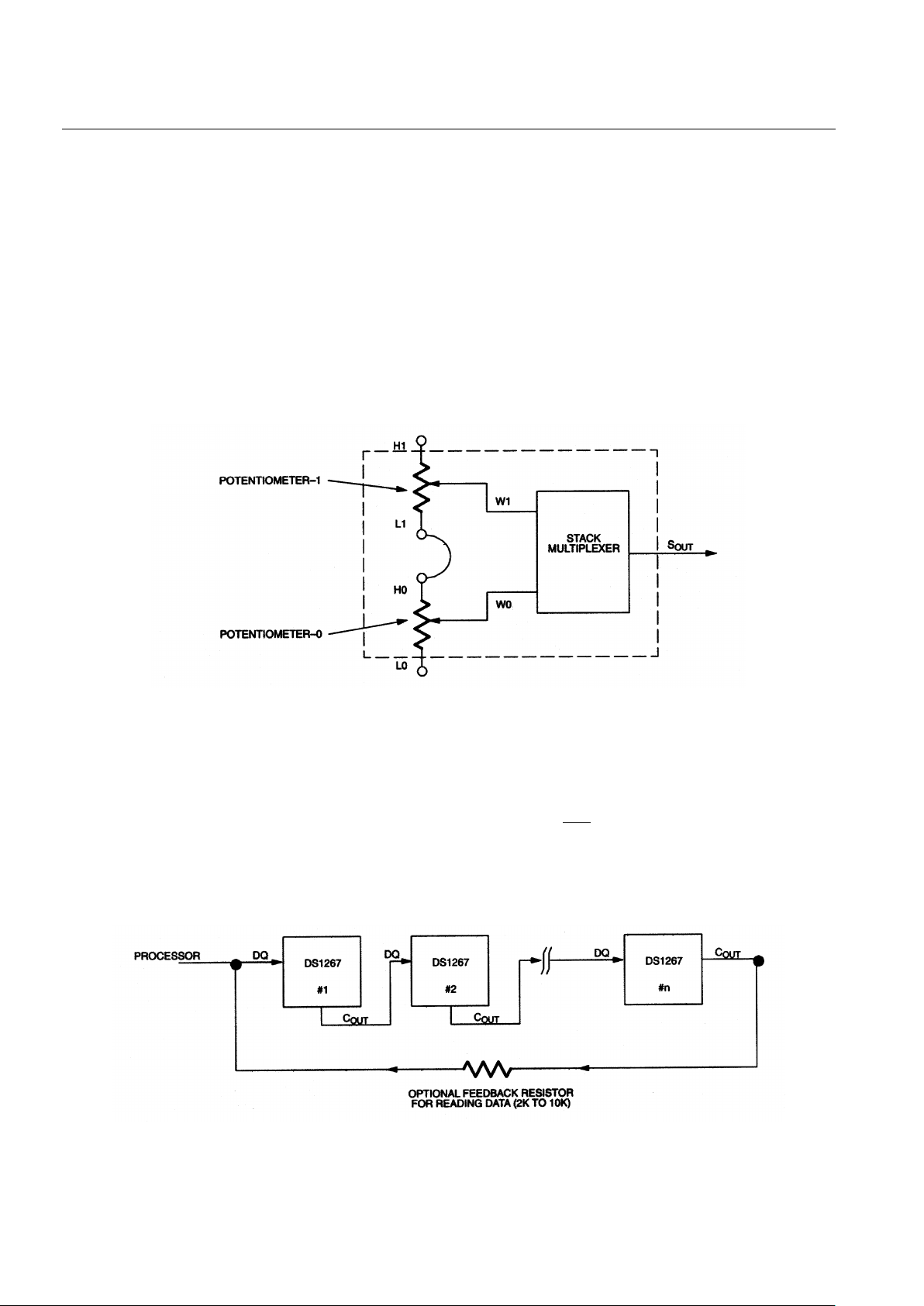
The potentiometers of the DS1267 can be connected in series as shown in Figure 3. This is referred to as
the stacked configuration. The stacked configuration allows the user to double the total end-to-end
resistance of the part and the number of steps to 512 (or 9 bits of resolution).
The wiper output for the combined stacked potentiometer will be taken at the S
OUT
pin, which is the
multiplexed output of the wiper of potentiometer-0 (W0) or potentiometer-1 (W1). The potentiometer
wiper selected at the S
OUT
output is governed by the setting of the stack select bit (bit 0) of the 17-bit I/O
shift register. If the stack select bit has value 0, the multiplexed output, S
OUT
, will be that of the
potentiometer-0 wiper. If the stack select bit has value 1, the multiplexed output, S
OUT
, will be that of the
potentiometer-1 wiper.
STACKED CONFIGURATION Figure 3
CASCADE OPERATION
A feature of the DS1267 is the ability to control multiple devices from a single processor. Multiple
DS1267s can be linked or daisy-chained as shown in Figure 4. As a data bit is entered into the I/O shift
register of the DS1267 a bit will appear at the C
OUT
output within a maximum delay of 50 nanoseconds.
The stack select bit of the DS1267 will always be the first out the part at the beginning of a transaction.
Additionally the C
OUT
pin is always active regardless of the state of RST . This allows one to read the I/O
shift register without changing its value.
CASCADING MULTIPLE DEVICES Figure 4
 Loading...