Dallas Semiconductor DS1238S-5, DS1238S-10, DS1238-5, DS1238-10N, DS1238-10 Datasheet

1 of 14 111899
FEATURES
Holds microprocessor in check during power
transients
Halts and restarts an out-of-control
microprocessor
Warns microprocessor of an impending power
failure
Converts CMOS SRAM into nonvolatile
memory
Unconditionally write-protects memory when
power supply is out of tolerance
Delays write protection until completion of
the current memory cycle
Consumes less than 200 nA of battery current
Controls external power switch for high
current applications
Debounces pushbutton reset
Accurate 10% power supply monitoring
Optional 5% power supply monitoring
designated DS1238-5
Provides orderly shutdown in microprocessor
applications
Pin-for-pin compatible with MAX691
Standard 16-pin DIP or space-saving 16-pin
SOIC
Optional industrial temperature range -40°C
to +85°C
PIN ASSIGNMENT
PIN DESCRIPTION
V
BAT
- +3-Volt Battery Input
V
CCO
- Switched SRAM Supply Output
VCC - +5-Volt Power Supply Input
GND - Ground
PF - Power-Fail
RVT - Reset Voltage Threshold
OSCIN - Oscillator In
OSCSEL - Oscillator Select
IN - Early Warning Input
NMI - Non-Maskable Interrupt
ST - Strobe Input
CEO - Chip Enable Output
CEI - Chip Enable Input
WDS - Watchdog Status
RST - Reset Output (active low)
RST - Reset Output (active high)
DESCRIPTION
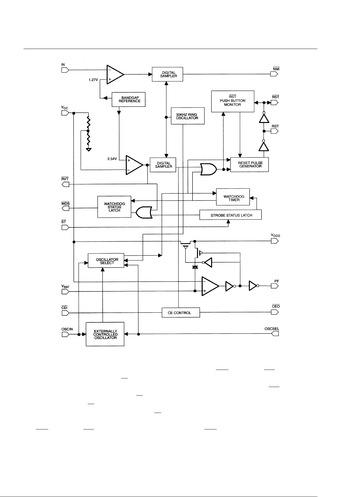
The DS1238 MicroManager provides all the necessary functions for power supply monitoring, reset
control, and memory backup in microprocessor-based systems. A precise internal voltage reference and
comparator circuit monitor power supply status. When an out-of-tolerance condition occurs, the
microprocessor reset and power-fail outputs are forced active, and static RAM control unconditionally
write protects external memory. The DS1238 also provides early warning detection of a user-defined
threshold by driving a non-maskable interrupt. External reset control is provided by a pushbutton reset
DS1238
MicroManage
r
www.dalsemi.com
16-Pin SOIC (300-mil)
See Mech. Drawings Section
VBAT
VCCO
VCC
RST
RST
WDS
1
2
3
16
15
14
GND CEI413
PF
RVT
OSCIN
CEO
ST
NMI
5
6
7
12
11
10
OSCSEL IN89
16-Pin DIP (300-mil)
See Mech. Drawings Section
VBAT
VCCO
VCC
RST
RST
WDS
1
2
3
16
15
14
GND CEI413
PF
RVT
OSCIN
CEO
ST
NMI
5
6
7
12
11
10
OSCSEL IN89

DS1238
2 of 14
debounce circuit connected to the RST pin. An internal watchdog timer can also force the reset outputs to
the active state if the strobe input is not driven low prior to watchdog timeout. Oscillator control pins
OSCSEL and OSCIN provide either external or internal clock timing for both the reset pulse width and
the watchdog timeout period. The Watchdog Status and Reset Voltage Threshold are provided via WDS
and RVT , respectively. A block diagram of the DS1238 is shown in Figure 1.
PIN DESCRIPTION
PIN NAME DESCRIPTION
V
BAT
+3V battery input provides nonvolatile operation of control functions.
V
CCO
VCC output for nonvolatile SRAM applications.
V
CC
+5V primary power input.
GND System ground.
PF
Power-fail indicator, active high, used for external power switching as shown in
Figure 9.
RVT
Reset Voltage Threshold. Indicates that VCC is below the reset voltage threshold.
OSCIN Oscillator input or timing capacitor. See Table 1.
OSCSEL Oscillator Select. Selects internal or external clock functions. See Table 1.
IN
Early warning power-fail input. This voltage sense point can be tied (via resistor
divider) to a user-selected voltage.
NMI
Non-maskable interrupt. Used in conjunction with the IN pin to indicate an impending
power failure.
ST
Strobe input. A high-to-low transition will reset the watchdog timer, indicating that
software is still in control.
CEO
Chip enable output. Write protected. Used with nonvolatile SRAM applications.
CEI
Chip enable input.
WDS
Watchdog Status. Indicates that a watchdog timeout has occurred.
RST
Active low reset output.
RST Active high reset output.
POWER MONITOR
The DS1238 employs a band gap voltage reference and a precision comparator to monitor the 5-volt
supply (VCC) in microprocessor-based systems. When an out-of-tolerance condition occurs, the RVT ,
RST, and RST outputs are driven to the active state. The VCC trip point (V
CCTP
) is set for 10% operation
so that the RVT , RST and RST outputs will become active as VCC falls below 4.5 volts (4.37 typical).
The V
CCTP
for the 5% operation option (DS1238-5) is set for 4.75 volts (4.62 typical). The RST and RST
signals are excellent for microprocessor reset control, as processing is stopped at the last possible moment
of in-tolerance VCC. On power up, RVT will become inactive as soon as VCC rises above V
CCTP
. However,
the RST and RST signals remain active for a minimum of 50 ms (100 ms typical) after V
CCTP
is reached
to allow the power supply and microprocessor to stabilize.

DS1238
3 of 14
DS1238 FUNCTIONAL BLOCK DIAGRAM Figure 1
WATCHDOG TIMER
The DS1238 provides a watchdog timer function which forces the WDS , RST, and RST signals to the
active state when the strobe input (ST) is not stimulated for a predetermined time period. This time period
is described below in Table 1. The watchdog timeout period begins as soon as RST and RST are inactive.
If a high-to-low transition occurs at t he ST input prior to timeout, the watchdog timer is reset and begins
to time out again. The ST input timing is shown in Figure 2. In order to guarantee that the watchdog timer
does not time out, a high-to-low transition on ST must occur at or less than the minimum timeout of the
watchdog as described in the AC Electrical Characteristics. If the watchdog timer is allowed to time out,
the WDS , RST, and RST outputs are driven t o the active state. WDS is a latched signal which indicates
the watchdog status, and is activated as soon as the watchdog timer completes a full period as outlined in

DS1238
4 of 14
Table 1. The WDS pin will remain low until one of three operations occurs. The first is to strobe the ST
pin with a falling edge, which will both set the WDS as well as the wat chdog timer count. The second is
to leave the ST pin open, which disables the watchdog. Lastly, the WDS pin is active low whenever V
CC
falls below V
CCTP
and activates the RVT signal. The ST input can be derived from microprocessor
address, data, or control signals, as well as microcontroller port pins. Under no rmal operating conditions,
these signals would routinely reset the watchdog timer prior to time out. The watchdog is disabled by
leaving the
ST input open, or as soon as V
CC
falls to V
CCTP
.
NON-MASKABLE INTERRUPT
The DS1238 generates a non-maskable interrupt ( NMI ) for early warning of a power failure to the
microprocessor. A precision comparator monitors the voltage level at the IN pin relative to an on-chip
reference generated by an internal band gap. The IN pin is a high impedance input allowing for a userdefined sense point. An external resistor voltage divider network (Figure 5) is used to interface with high
voltage signals. This sense point may be derived from the regulated 5-volt supply, or from a higher DC
voltage level closer to the main system power input. Since the IN trip point VTP is 1.27 volts, the proper
values for R1 and R2 can be determined by the equation as shown in Figure 5. Proper operation of the
DS1238 requires that the voltage at the IN pin be limited to V
IH
. Therefore, the maximum allowable
voltage at the supply being monitored (V
MAX
) can also be derived as shown in Figure 5. A simple
approach to solving this equation is to select a value for R2 of high enough value to keep power
consumption low and solve for R1. The flexibility of the IN input pin allows for detection of power loss
at the earliest point in a power supply system, maximizing the amount of time for microprocessor
shutdown between NMI and RST or RST .
When the supply being monitored decays to the voltage sense point, the DS1238 will force the NMI
output to an active state. Noise is removed from the NMI power-fail detection circuitry using built-in
time domain hysteresis. That is, the monitored supply is sampled periodically at a rate determined by an
internal ring oscillator running at approximately 30kHz (33 µs/cycle). Three consecutive samplings of
out-of-tolerance supply (below V
SENSE
) must occur at the IN pin to active NMI . Therefore, the suppl y
must be below the voltage sense point for approximately 100 µs or the comparator will reset. In this way,
power supply noise is removed from the monitoring function preventing false trips. During a power-up,
any IN pin levels below VTP detected by the compa rator are disabled from reaching the NMI I pin until
V
CC
rises to V
CCTP
. As a result, any potential active NMI will not be initiated until VCC reaches V
CCTP
.
Removal of an active low level on the
NMI pin is controlled by the subsequent rise of the IN pin above
VTP. The initiation and removal of the NMI signal during power up depends on the relative voltage
relationship between VCC and the IN pin voltage. Note that a fast-slewing power supply may cause the
NMI to be virtually nonexistent on power up. This is of no consequence, however, since an RST will be
active. The NMI voltage will follow VCC down until VCC decays to V
BAT
. Once VCC decays to VBAT , the
NMI pin will enter a tri-state mode.
ST INPUT TIMING Figure 2

DS1238
5 of 14
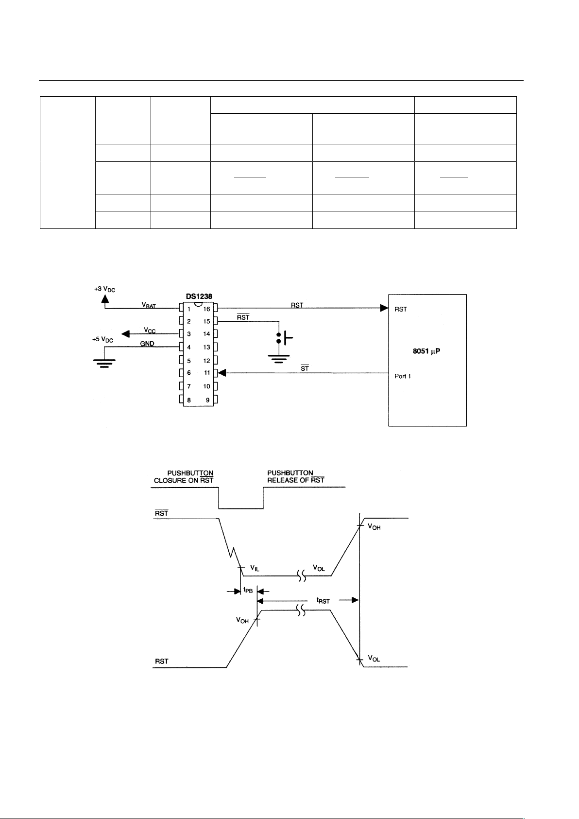
OSCILLATOR CONTROLS Table 1
Watchdog Timeout Period (typ)
OSCIN OSCSEL
First Period
Following a Reset
Other Timeout
Reset Active
Duration
Ext Clk Low 20480 Clks 5120 Clocks 641 Clks
Ext Cap Low
≅
pf 47
sec2.2
X Cpf ≅
pf 47
ms550
X Cpf ≅
pf 47
ms 69
X Cpf
Low Hi/Open 2.7 sec 170 ms 85 ms
External
Internal
Hi/Open Hi/Open 2.7 sec 2.7 sec 85 ms
Note that the OSCIN and OSCSEL pins are tri-stated when VCC is below V
BAT
.
POWER MONITOR, WATCHDOG TIMER, AND PUSHBUTTON RESET Figure 3
PUSHBUTTON RESET TIMING Figure 4
 Loading...