

dallas semiconductor DS1135L service manual
www.maxim-ic.com
DS1135L
3V 3-in-1 High-Speed
Silicon Delay Line
FEATURES
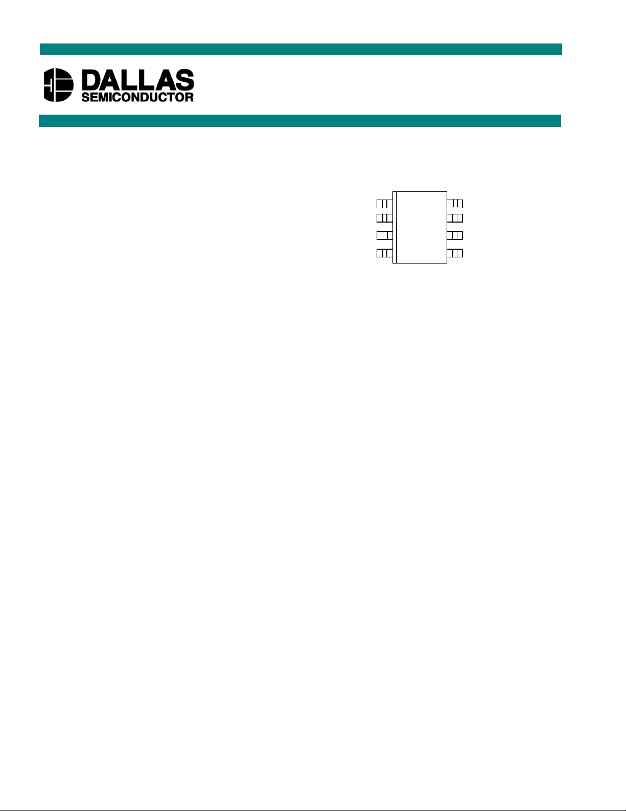
PIN ASSIGNMENT
§ All-silicon timing circuit
§ Three independent buffered delays
§ Stable and precise over temperature and
voltage
§ Leading and trailing edge precision preserves
the input symmetry
§ Standard 8-pin SO
(150mil), and 8-Pin µSOP (118mil)
§ Vapor phase and IR reflow solderable
§ Available in Tape and Reel
§ Delays specified over both commercial and
IN1
IN2
IN3
GND
1
2
3
4
DS1135LZ 8-Pin SO (150mil)
DS1135LU 8-Pin µSOP (118mil)
See Mech. Drawings Section
8
V
CC
7
OUT1
6
OUT2
5
OUT3
industrial temperature ranges
§ 3V operation
§ Recommended replacement for DS1033
PIN DESCRIPTION
IN1-IN3 - Input Signals
OUT1-OUT3 - Output Signals
V
CC
- +3V Supply
GND - Ground
DESCRIPTION
The DS1135L series is a low-power, 3V high-speed version of the popular DS1013, DS1033, DS1035
series.
The DS1135L series of delay lines have three independent logic buffered delays in a single package. The
device is Dallas Semiconductor’s fastest 3-in-1 delay line. It is available in a standard 8-pin 118mil
µSOP and 150mil 8-pin Mini-SO.
The device features precise leading and trailing edge accuracy. It has the inherent reliability of an allsilicon delay line solution.
Standard delay values are indicated in Table 1. Customers may contact Dallas Semiconductor at (972)
371-4348 for further information on custom delay values.
1 of 6 011402
LOGIC DIAGRAM Figure 1
DS1135-L
TIME DELAY
ONE OF THREE
PART NUMBER DELAY TABLE (t
DELAY PER
OUTPUT
PART NUMBER
DS1135LX-10 10/10/10
DS1135LX-12 12/12/12
DS1135LX-15 15/15/15
DS1135LX-20 20/20/20
DS1135LX-25 25/25/25
DS1135LX-30 30/30/30
(ns)
, t
PLH
INITIAL
TOLERANCE
(Note 1)
±1.0ns ±2.0ns ±3.0ns
±1.0ns ±2.0ns ±3.0ns
±1.0ns ±2.5ns ±4.0ns
±1.0ns ±2.5ns ±4.0ns
±1.5ns ±3.0ns ±5.0ns
±1.5ns ±3.0ns ±5.0ns
NOTES:
1. Nominal conditions are +25°C and VCC = +3.3V.
) Table 1
PHL
OUTIN
TOLERANCE OVER
TEMP AND VOLTAGE
(Note 2)
0°C to +70°C -40°C to +85°C
2. Voltage range of 2.7V to 3.6V.
3. Delay accuracies is for both leading and trailing edges.
4. X in Part number denotes package: U indicates µSOP, Z indicates SO.
TEST SETUP DESCRIPTION
Figure 2 illustrates the hardware configuration used for measuring the timing parameters of the DS1135L.
The input waveform is produced by a precision pulse generator under software control. Time delays are
measured by a time interval counter (20 ps resolution) connected to the output. The DS1135L output taps
are selected and connected to the interval counter by a VHF switch control unit. All measurements are
fully automated with each instrument controlled by the computer over an IEEE 488 bus.
2 of 6
 Loading...