dallas semiconductor DS1065 service manual

DS1065
EconOscillator/Divider
www.dalsemi.com
VIEW
Dallas
1 2 3
查询DS1065T-060供应商
FEATURES
PIN ASSIGNMENT
§ 30 kHz to 100 MHz output frequencies
§ User-programmable on-chip dividers (from 1-
DS1065
513)
§ User-programmable on-chip prescaler (1, 2,
4)
§ No external components
§ ±0.5% initial tolerance
§ ±3% variation over temperature and voltage
1 2 3
§ Single 5V supply
FREQUENCY OPTIONS
BOTTOM
Part No. Max O/P freq.
DS1065-100 100.000 MHz
DS1065-80 80.000 MHz
DS1065-66 66.667 MHz
DS1065-60 60.000 MHz
PIN DESCRIPTION
TO-92
1 I/O - Input/Output
2 V
CC
- Power Supply
3 GND - Ground
DESCRIPTION
The DS1065 is a fixed frequency oscillator requiring no external components for operation. Numerous
operating frequencies are possible in the range of approximately 30 kHz to 100 MHz through the use of
an on-chip programmable prescaler and divider.
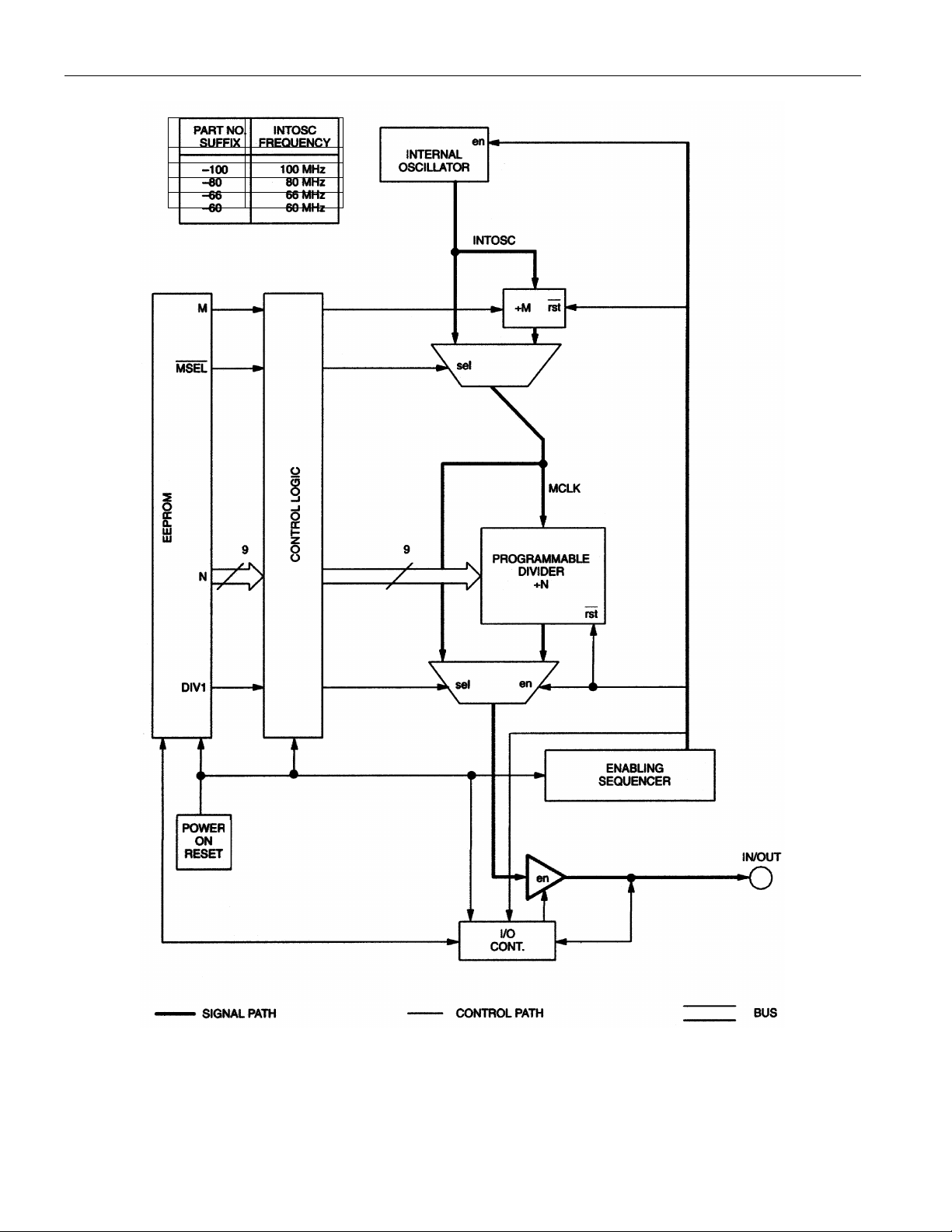
The DS1065 features a master oscillator followed by a prescaler and then a programmable divider. The
prescaler and programmable divider are user-programmable with the desired values being stored in
nonvolatile memory. This allows the user to buy an off the shelf component and program it on site prior
to board production. Design changes can be accommodated easily by simply programming different
values into the device (or reprogramming previously programmed devices). The DS1065 is shipped from
the factory configured for half the maximum operating frequency. Contact the factory for specially
programmed devices.
The DS1065 features a dual-purpose Input/Output pin. If the device is powered up in Program mode this
pin can be used to input serial data to the on-chip registers. After a write command this data is stored in
nonvolatile memory. When the chip is subsequently powered up in operating mode these values are
automatically restored to the on-chip registers and the Input/Output pin becomes the oscillator output.
The DS1065 is available in TO-92 (3 LEAD) package, allowing the generation of a clock signal easily,
economically and using minimal board area.
1 of 10 093099

BLOCK DIAGRAM Figure 1
DS1065
PART NO.
SUFFIX
-100 100.000 MHz
-80 80.000 MHz
-66 66.667 MHz
-60 60.000 MHz
INTOSC
FREQUENCY
2 of 10

DS1065
PIN DESCRIPTIONS
Input/Output Pin (IN/OUT): This pin is the main oscillator output, with a frequency determined by
clock reference, M and N dividers. Except in programming mode this pin is always an output and will be
referred to as “OUT”. In programming mode this pin will be referred to as “IN”.
USER-PROGRAMMABLE REGISTERS
The following registers can be programmed by the user to determine device operating frequency and
mode of operation. Details of how these registers are programmed can be found in a later section; in this
section the function of the registers are described. The register settings are nonvolatile, the values being
stored automatically in EEPROM when the registers are programmed.
NOTE: The register bits cannot be used to make frequency changes on the fly. Changes can only be
made by powering the device up in “Programming” mode. For them to be become effective the device
must then be powered down and powered up again in “Operation” mode.
For programming purposes the register bits are divided into two 9-bit words; the “MUX” word
determines mode prescaler values and the “DIV” word sets the value of the programmable divider.
MUX WORD Figure 2
(MSB) (LSB)
0* 0* 0* 1* 1* M
MSEL
DIV1 0*
*These bits must be set to the indicated values
DIV1
This bit allows the master clock to be routed directly to the output (DIV1=1). The N programmable
divider is bypassed so the programmed value of N is ignored. The frequency of the output (f
) will be
OUT
INTCLK or EXTCLK depending on which reference has been selected. If the Internal clock is selected
the M prescaler is also bypassed (the bit values of MSEL and M are ignored), so in this case f
OUT
=
INTOSC (which also equals MCLK and INTCLK). If DIV1=0 the prescaler and programmable divider
function normally.
MSEL
This bit determines whether or not the M prescaler is bypassed. MSEL =1 will bypass the prescaler.
MSEL =0 will switch in the prescaler (unless overridden by DIV1=1), with a divide-by number
determined by the M bit.
M
This bit sets the divide-by number for the prescaler. M = 0 results in divide-by-4, M=1 results in divideby-2. The setting of this bit is irrelevant if either DIV1=1 or MSEL =1.
Table 2
DIV1
BIT
MSEL
BIT
0 0 0 INTERNAL OSCILLATOR DIVIDED BY 4*N
0 0 1 INTERNAL OSCILLATOR DIVIDED BY 2*N
0 1 X INTERNAL OSCILLATOR DIVIDED BY N
M
BIT OPERATION
3 of 10
 Loading...