dallas semiconductor DS1012 service manual

查询DS1012供应商
DS1012
DS1012
2-in-1 Sub-Miniature Silicon
Delay Line with Logic
FEATURES
• All-silicon time delay
• 53 µW max. CMOS quiescent mode
• Surface mount 8-pin mini-SOIC and standard 8-pin
DIP
• 2 independent buffered delays per input
• Option of complemented output(s)
• Option of timed AND, NAND, OR, NOR, XOR, XNOR,
HALF-XOR and HALF-XNOR logic outputs
• Delay tolerance: ±1.5 ns (delays: 3-10 ns),
±2.0 ns (delays: 11-40 ns)
• Vapor phase, IR and wave solderability
• Economical
• TTL/CMOS-compatible
• Quick turn prototypes
• Custom delays and logic options available
DESCRIPTION
In its most simple configuration, the DS1012 2-in-1
Sub-Miniature Silicon Delay Line Chip provides two inputs, each of which in turn provides independent delays
to a pair of outputs. The DS1012-1 and DS1012-3 are
examples of catalog parts having this basic configuration. Any of the four outputs can be inverted at the time
of manufacture.
For applications requiring two-input timed logic functions, at the time of manufacture the simple delay on
OUT4 can be replaced by one of the following: OR,
NOR, XOR, or XNOR. Similarly, a timed AND, NAND,
HALF-XOR (D3 AND D4
D4) can be substituted for the simple delay on OUT3.
DS1012-2, DS1012-4, and DS1012-5 are examples of
), or NOT HALF-XOR (D3 OR
PIN ASSIGNMENT
IN1
1
8
V
2
OUT3
OUT1
3
GND
4
DS1012M 8-PIN DIP (300 MIL)
See Mech. Drawings
Section
1
IN1
OUT3
OUT1
GND
2
3
4
DS1012Z 8-PIN SOIC (150 MIL)
See Mech. Drawings
Section
CC
7
IN2
OUT2
6
5
OUT4
8
V
CC
7
IN2
6
OUT2
5
OUT4
PIN DESCRIPTION
IN1, IN2 – Inputs
OUT1, OUT2 – Outputs (delays)
OUT3, OUT4 – Outputs (delays, logic)
GND – Ground
V
CC
catalog parts configured with logic functions on OUT3
and OUT4. Note that DS1012-2 also utilizes an output
inversion on OUT2.
In any configuration, delays D1 (t
specified within the range of ~3 ns to 10 ns. Delays D3
(tD3) and D4 (tD4) can be specified to have values between ~3 ns and 40 ns. The worst case leading edge
delay accuracy at nominal voltage and room temperature is ±2 ns. The DS1012 is offered in two packages: an
8-pin DIP and an 8-pin 150 mil wide mini-SOIC.
Dallas Semiconductor offers the DS1012 in a wide variety of custom delay and logic configurations. For special
requests and quick turn delivery, call (972) 371–4348.
– +5 Volts
) and D2 (tD2) can be
D1
021798 1/7

DS1012
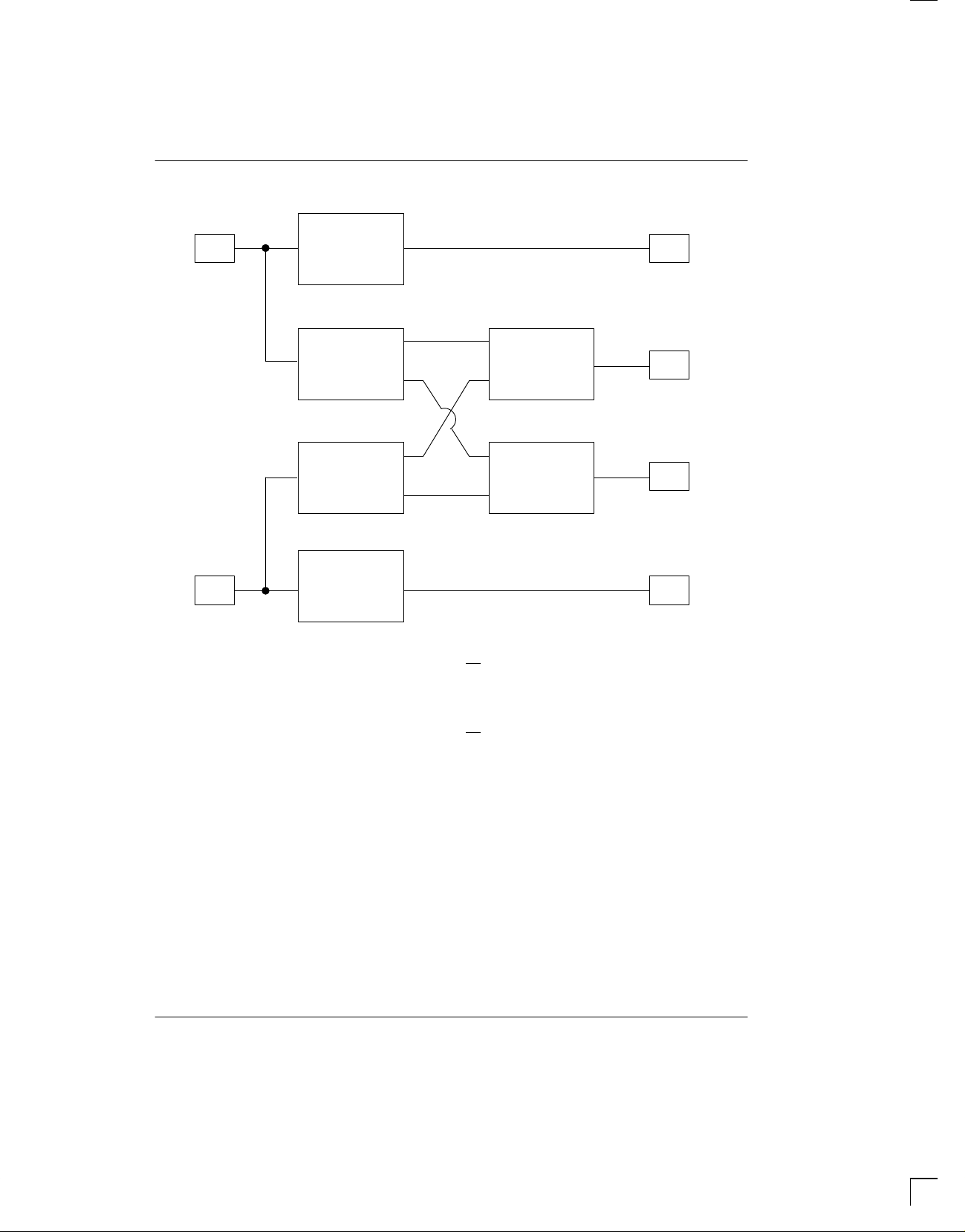
LOGIC DIAGRAM Figure 1
IN1
IN2
DELAY
D1
DELAY
D3
DELAY
D4
DELAY
D2
Function f3 can be one of the following:
D3
D3 AND D4
D3 HALF-XOR D4
Function f4 can be one of the following:
D4
D3 OR D4
D3 XOR D4
FUNCTION
f3
FUNCTION
f4
D3
D3 NAND D4
D3 HALF-XNOR D4
D4
D3 NOR D4
D3 XNOR D4
OUT1
OUT3
OUT4
OUT2
NOTE: Any output(s) can be inverted at time of manufacture.
If D1 > 10 ns, D1 = D3.
If D2 > 10 ns, D2 = D4.
021798 2/7

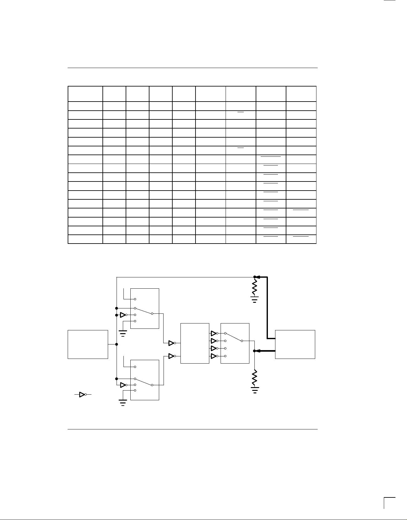
PART NUMBER DELAY AND CONFIGURATION Table 1
CATALOG
P/N
DS1012-1 5 5 10 10 D1 D2 D3 D4
DS1012-2 5 5 10 10 D1 D2 D3.D4 D3+D4
DS1012-3 3 7 10 40 D1 D2 D3 D4
DS1012-4 5 5 25 25 D1 D2 D3HXD4 D3XD4
DS1012-5 10 10 5 5 D1 D2 D3.D4 D3+D4
DS1012-7 15 4 4 14 D1 D2 D3 D3XD4
DS1012–9 5 25 5 25 D1 D2 D3HXD4 D3XD4
DS1012-D16 4 19.6 4 19.6 D1 D2 D3.D4 D3XD4
DS1012-D20 4 16.5 4 16.5 D1 D2 D3.D4 D3XD4
DS1012-D25 4 14 4 14 D1 D2 D3.D4 D3XD4
DS1012-D33 4 11.5 4 11.5 D1 D2 D3.D4 D3XD4
DS1012-D50 4 9 4 9 D1 D2 D3.D4 D3XD4
DS1012-V20 25 50 25 50 D1 D2 D3.D4 D3+D4
DS1012-V40 12.5 25 12.5 25 D1 D2 D3.D4 D3XD4
DS1012-V50 10 20 10 20 D1 D2 D3.D4 D3XD4
DS1012-V60 8.3 8.3 8.3 8.3 D1 D2 D3.D4 D3+D4
t
D1
(ns)
t
D2
(ns)
t
D3
(ns)
t
D4
(ns)
OUT1 OUT2 OUT3 OUT4
DS1012
NOTE: . = AND, + = OR, X = XOR, HX = HALF–XOR
Contact Dallas Semiconductor for information on custom configurations and timing delays.
TEST CIRCUIT Figure 2
PULSE
GENERATOR
74F04
+5V
+5V
CONTROL UNIT
VHF SWITCH
UNDER
TEST
= 50 Ω
Z
0
VHFDEVICE
SWITCH
CONTROL
UNIT
STOP
TIP
Z
0
= 50 Ω
START TIP
(TIME INTERVAL
PROBE)
TIME
INTERVAL
COUNTER
021798 3/7
 Loading...