

Dallas Maxim DS12885, Maxim DS12887A, Maxim DS12C887A, Maxim DS12C887, Maxim DS12887 User Manual
General Description
The DS12885, DS12887, and DS12C887 real-time
clocks (RTCs) are designed to be direct replacements
for the DS1285 and DS1287. The devices provide a
real-time clock/calendar, one time-of-day alarm, three
maskable interrupts with a common interrupt output, a
programmable square wave, and 114 bytes of batterybacked static RAM (113 bytes in the DS12C887 and
DS12C887A). The DS12887 integrates a quartz crystal
and lithium energy source into a 24-pin encapsulated
DIP package. The DS12C887 adds a century byte at
address 32h. For all devices, the date at the end of the
month is automatically adjusted for months with fewer
than 31 days, including correction for leap years. The
devices also operate in either 24-hour or
12-hour format with an AM/PM indicator. A precision
temperature-compensated circuit monitors the status of
VCC. If a primary power failure is detected, the device
automatically switches to a backup supply. A lithium
coin-cell battery can be connected to the V
BAT
input
pin on the DS12885 to maintain time and date operation
when primary power is absent. The device is accessed
through a multiplexed byte-wide interface, which supports both Intel and Motorola modes.
Applications
Embedded Systems
Utility Meters
Security Systems
Network Hubs, Bridges, and Routers
Features
♦ Drop-In Replacement for IBM AT Computer
Clock/Calendar
♦ RTC Counts Seconds, Minutes, Hours, Day, Date,
Month, and Year with Leap Year Compensation
Through 2099
♦ Binary or BCD Time Representation
♦ 12-Hour or 24-Hour Clock with AM and PM in
12-Hour Mode
♦ Daylight Saving Time Option
♦ Selectable Intel or Motorola Bus Timing
♦ Interfaced with Software as 128 RAM Locations
♦ 14 Bytes of Clock and Control Registers
♦ 114 Bytes of General-Purpose, Battery-Backed
RAM (113 Bytes in the DS12C887 and
DS12C887A)
♦ RAM Clear Function (DS12885, DS12887A, and
DS12C887A)
♦ Interrupt Output with Three Independently
Maskable Interrupt Flags
♦ Time-of-Day Alarm Once Per Second to Once
Per Day
♦ Periodic Rates from 122μs to 500ms
♦ End-of-Clock Update Cycle Flag
♦ Programmable Square-Wave Output
♦ Automatic Power-Fail Detect and Switch Circuitry
♦ Optional 28-Pin PLCC Surface Mount Package or
32-Pin TQFP (DS12885)
♦ Optional Encapsulated DIP (EDIP) Package with
Integrated Crystal and Battery (DS12887,
DS12887A, DS12C887, DS12C887A)
♦ Optional Industrial Temperature Range Available
♦ Underwriters Laboratory (UL) Recognized
DS12885/DS12887/DS12887A/DS12C887/DS12C887A
Real-Time Clock
______________________________________________
Maxim Integrated Products
1
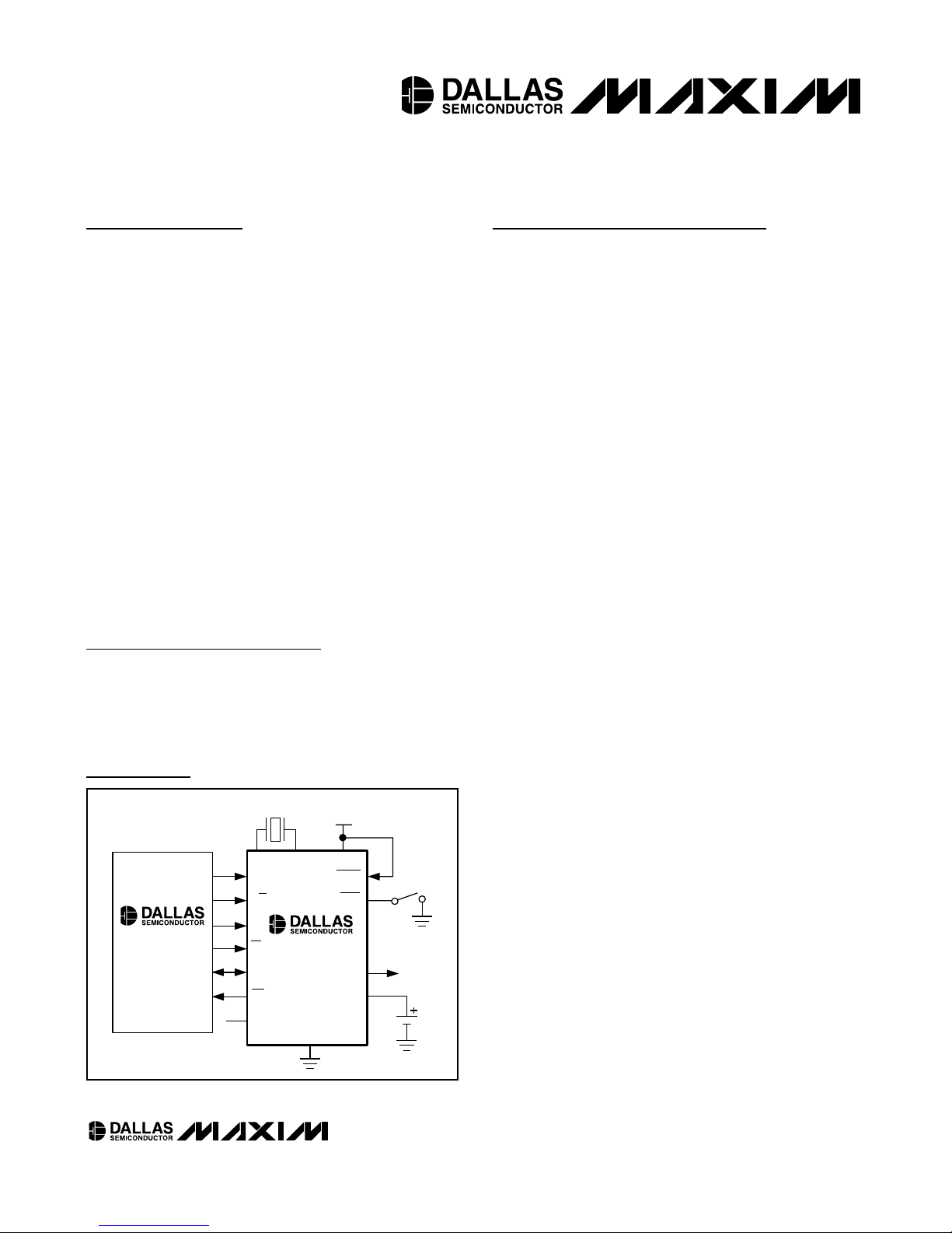
Typical Operating Circuit
Rev 3; 2/07
For pricing, delivery, and ordering information, please contact Maxim/Dallas Direct! at
1-888-629-4642, or visit Maxim’s website at www.maxim-ic.com.
Pin Configurations and Ordering Information appear at end of data sheet.
DS83C520
CRYSTAL
AS
R/W
DS
CS
AD(0–7) SQW
IRQ
MOT
X2X1
DS12885
GND
V
CC
V
CC
RESET
RCLR
V
BAT
DS12885/DS12887/DS12887A/DS12C887/DS12C887A
Real-Time Clock
2 _____________________________________________________________________
ABSOLUTE MAXIMUM RATINGS
Stresses beyond those listed under “Absolute Maximum Ratings” may cause permanent damage to the device. These are stress ratings only, and functional
operation of the device at these or any other conditions beyond those indicated in the operational sections of the specifications is not implied. Exposure to
absolute maximum rating conditions for extended periods may affect device reliability.
Voltage Range on VCCPin Relative to Ground .....-0.3V to +6.0V
Operating Temperature Range ...................................................
Commercial (noncondensing) .............................0°C to +70°C
Operating Temperature Range ...................................................
Industrial (noncondensing)...............................-40°C to +85°C
Storage Temperature Range .............................-55°C to +125°C
Soldering Temperature .......................................See IPC/JEDEC
J-STD-020 Specification (Note 1)
Soldering Temperature (leads, 10s) ................................+260°C
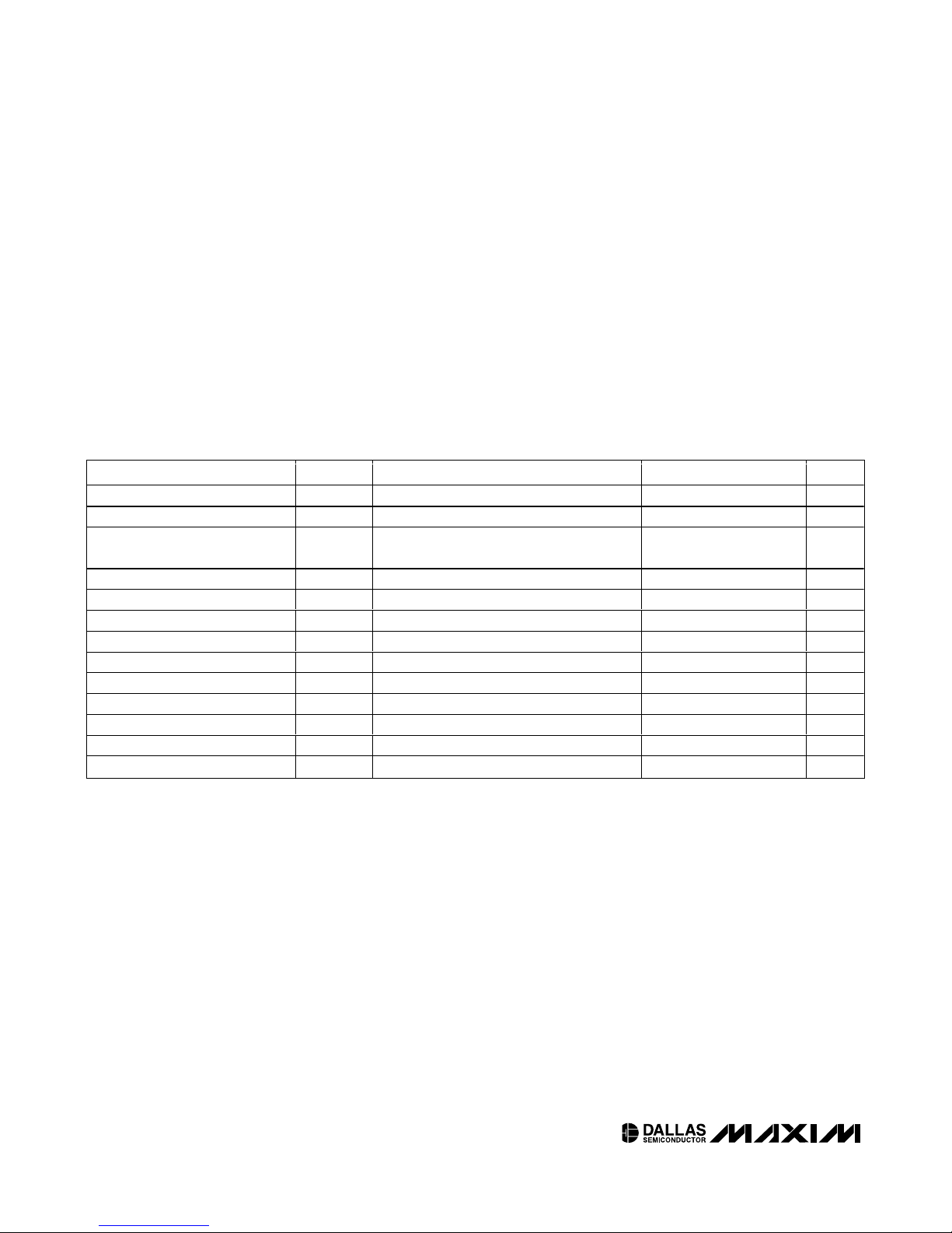
DC ELECTRICAL CHARACTERISTICS
(V
CC
= +4.5V to +5.5V, TA= over the operating range, unless otherwise noted.) (Note 2)
Supply Voltage V
V
BAT
Input Logic 1 V
Input Logic 0 V
VCC Power-Supply Current I
VCC Standby Current I
Input Leakage I
I/O Leakage I
Input Current I
Output at 2.4V I
Output at 0.4V I
Power-Fail Voltage V
VRT Trip Point VRT
PARAMETER SYMBOL CONDITIONS MIN TYP MAX UNITS
(Note 3) 4.5 5.5 V
(Note 3) 2.5 4.0 V
(Note 3) 2.2
IH
(Note 3) -0.3 +0.8 V
IL
(Note 4) 15 mA
(Note 5) mA
IL
(Note 6) -1.0 +1.0 µA
(Note 7) -1.0 +500 µA
(Note 3) -1.0 mA
(Note 3) 4.0 mA
(Note 3) 4.0 4.25 4.5 V
PF
TRIP
Input Voltage V
CC
BAT
CC1
CCS
OL
MOT
OH
OL
V
+
CC
0.3
-1.0 +1.0 µA
1.3 V
V
DS12885/DS12887/DS12887A/DS12C887/DS12C887A
Real-Time Clock
_____________________________________________________________________ 3
DC ELECTRICAL CHARACTERISTICS
(VCC= 0V, V
BAT
= 3.0V, TA= over the operating range, unless otherwise noted.) (Note 2)
AC ELECTRICAL CHARACTERISTICS
(VCC= 4.5V to 5.5V, TA= over the operating range.) (Note 2)
V
Current (OSC On);
BAT
T
= +25°C, V
A
V
Current (Oscillator Off) I
BAT
PARAMETER SYMBOL CONDITIONS MIN TYP MAX UNITS
BACKUP
= 3.0V
I
BAT
BATDR
(Note 8) 500 nA
(Note 8) 100 nA
PARAMETER SYMBOL CONDITIONS MIN TYP MAX UNITS
Cycle Time t
Pulse Width, DS Low or R/W High PW
Pulse Width, DS High or R/W Low PW
Input Rise and Fall tR, t
R/W Hold Time t
R/W Setup Time Before DS/E t
Chip-Select Setup Time Before
DS or R/W
Chip-Select Hold Time t
Read-Data Hold Time t
Write-Data Hold Time t
Address Valid Time to AS Fall t
Address Hold Time to AS Fall t
Delay Time DS/E to AS Rise t
Pulse Width AS High PW
Delay Time, AS to DS/E Rise t
Output Data Delay Time from DS
or R/W
Data Setup Time t
Reset Pulse Width t
IRQ Release from DS t
IRQ Release from RESET t
CYC
EL
EH
RWH
RWS
t
CS
CH
DHR
DHW
ASL
AHL
ASD
ASH
ASED
t
DDR
DSW
RWL
IRDS
IRR
F
385 DC ns
150 ns
125 ns
30 ns
10 ns
50 ns
20 ns
0ns
10 80 ns
0ns
30 ns
10 ns
20 ns
60 ns
40 ns
20 120 ns
100 ns
5µs
2µs
2µs
DS12885/DS12887/DS12887A/DS12C887/DS12C887A
Real-Time Clock
4 _____________________________________________________________________
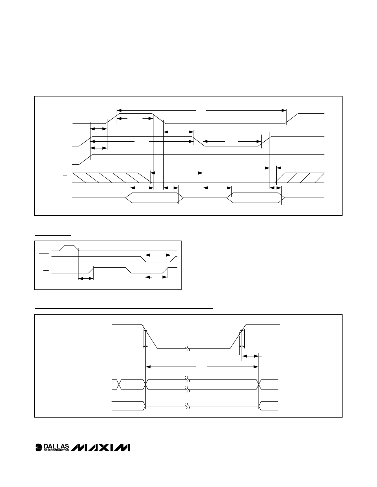
Motorola Bus Read/Write Timing
Intel Bus Write Timing
PW
ASH
PW
EL
PW
EH
t
CS
t
AHL
t
ASL
t
DSW
t
DHW
t
CH
t
ASD
t
ASD
t
CYC
CS
R/W
AS
DS
AD0–AD7
WRITE
t
ASED
AS
t
ASD
PW
ASH
t
ASED
t
CYC
DS
R/ W
CS
AD0–AD7
WRITE
AD0–AD7
READ
PW
PW
t
DDR
EH
t
RWH
t
CH
t
DSW
t
t
DHW
DHR
EL
t
RWS
t
CS
t
ASL
t
AHL
DS12885/DS12887/DS12887A/DS12C887/DS12C887A
Real-Time Clock
_____________________________________________________________________ 5
Intel Bus Read Timing
t
RWL
t
IRR
t
IRDS
DS
RESET
IRQ
IRQ
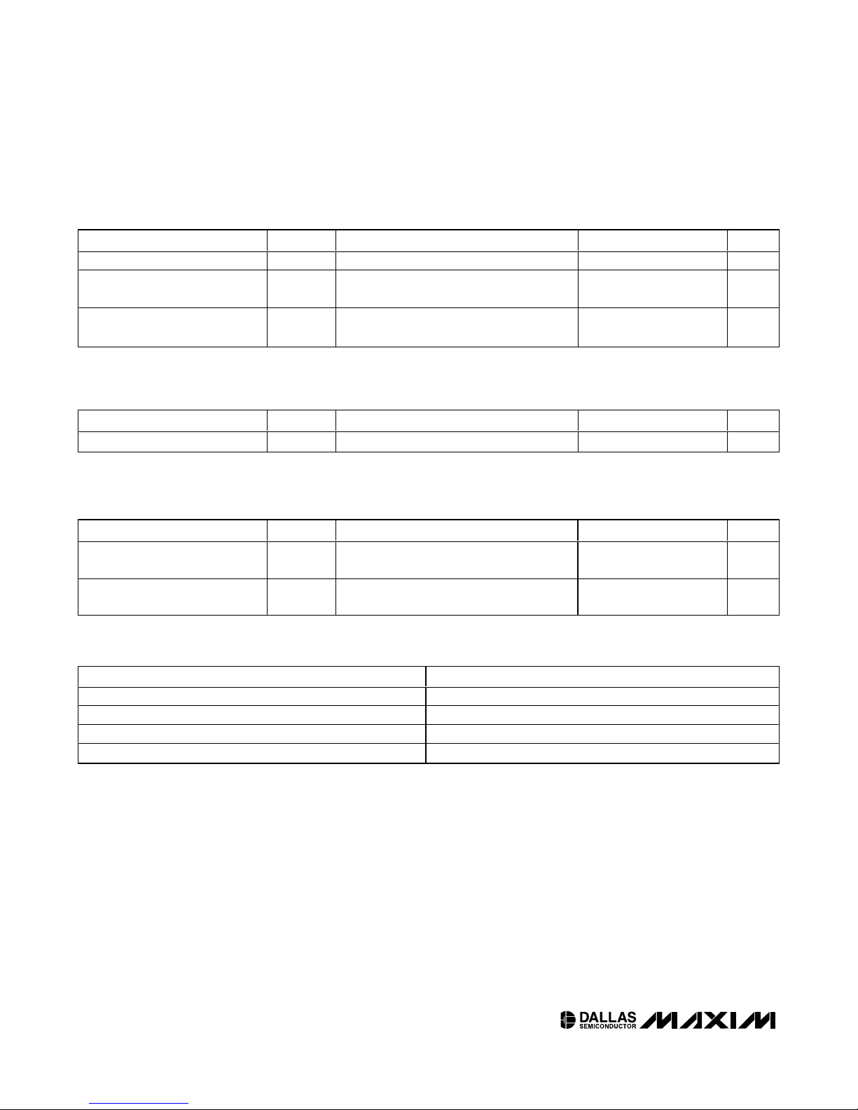
Release Delay Timing
OUTPUTS
INPUTS
HIGH-Z
DON'T CARE
VALID
RECOGNIZED
RECOGNIZED
VALID
V
CC
t
F
V
PF(MAX)
V
PF(MIN)
t
RPU
t
R
t
DR
Power-Up/Power-Down Timing
R/W
AD0–AD7
AS
DS
CS
PW
ASH
t
ASD
PW
t
ASD
EL
t
ASL
t
ASED
t
CS
t
CYC
PW
EH
t
CH
t
AHL
t
DDR
t
DHR
DS12885/DS12887/DS12887A/DS12C887/DS12C887A
Real-Time Clock
6 _____________________________________________________________________
POWER-UP/POWER-DOWN CHARACTERISTICS
(TA= -40°C to +85°C) (Note 2)
CAPACITANCE
(TA= +25°C) (Note 9)
DATA RETENTION
(TA= +25°C)
AC TEST CONDITIONS
WARNING: Negative undershoots below -0.3V while the part is in battery-backed mode may cause loss of data.
Note 1: RTC modules can be successfully processed through conventional wave-soldering techniques as long as temperature
exposure to the lithium energy source contained within does not exceed +85°C. However, post-solder cleaning with waterwashing techniques is acceptable, provided that ultrasonic vibrations are not used to prevent crystal damage.
Note 2: Limits at -40°C are guaranteed by design and not production tested.
Note 3: All voltages are referenced to ground.
Note 4: All outputs are open.
Note 5: Specified with CS = DS = R/W = RESET = V
CC
; MOT, AS, AD0–AD7 = 0; V
BACKUP
open.
Note 6: Applies to the AD0 to AD7 pins, the IRQ pin, and the SQW pin when each is in a high-impedance state.
Note 7: The MOT pin has an internal 20kΩ pulldown.
Note 8: Measured with a 32.768kHz crystal attached to X1 and X2.
Note 9: Guaranteed by design. Not production tested.
Note 10: Measured with a 50pF capacitance load.
Recovery at Power-Up t
VCC Fall Time; V
V
PF(MIN)
VCC Rise Time; V
V
PF(MAX)
Expected Data Retention t
Capacitance on All Input Pins
Except X1 and X2
Capacitance on IRQ, SQW, and
DQ Pins
PARAMETER SYMBOL CONDITIONS MIN TYP MAX UNITS
RPU
PF(MIN)
to
to
C
C
t
t
DR
F
R
IN
IO
PF(MAX)
PARAMETER SYMBOL CONDITIONS MIN TYP MAX UNITS
PARAMETER SYMBOL CONDITIONS MIN TYP MAX UNITS
20 200 ms
300 µs
0µs
10 years
5pF
7pF
PARAMETER TEST CONDITIONS
Input Pulse Levels 0 to 3.0V
Output Load Including Scope and Jig 50pF + 1TTL Gate
Input and Output Timing Measurement Reference Levels Input/Output: VIL maximum and VIH minimum
Input-Pulse Rise and Fall Times 5ns
DS12885/DS12887/DS12887A/DS12C887/DS12C887A
Real-Time Clock
_____________________________________________________________________
7
Typical Operating Characteristics
(VCC= +5.0V, TA= +25°C, unless otherwise noted.)
OSCILLATOR FREQUENCY
vs. V
CC
DS12885 toc02
VCC (V)
FREQUENCY (Hz)
5.3
5.04.8
32768.10
32768.20
32768.30
32768.40
32768.50
32768.60
32768.70
32768.00
4.5 5.5
I
BAT1
vs. V
BAT
vs. TEMPERATURE
DS12885 toc01
V
BAT
(V)
I
BAT
(nA)
3.82.8
3.0
3.3
3.5
200
300
250
150
2.5
4.0
VCC = 0V
+85°C
+25°C
0°C
-40°C
+70°C
+40°C
Functional Diagram
X1
X2
V
CC
GND
V
BAT
CS
R/W
DS
RESET
AD0–AD7
AS
MOT
RLCR
OSC
POWER
CONTROL
BUS
INTERFACE
DIVIDE
BY 8
DS12885
CLOCK/CALENDAR
UPDATE LOGIC
DIVIDE
BY 64
16:1 MUX
DIVIDE
BY 64
SQUARE-
WAVE
GENERATOR
IRQ
GENERATOR
REGISTERS A, B, C, D
CLOCK/CALENDAR AND
ALARM REGISTERS
BUFFERED CLOCK/
CALENDAR AND ALARM
REGISTERS
USER RAM
114 BYTES
SQW
IRQ
 Loading...