

Dallas DS87C550 User Manual Supplement

DS87C550
High-Speed Microcontroller
User’s Guide Supplement
www.dalsemi.com
Section 1:Introduction
This document is provided as a supplement to the High-Speed Microcontrollers User’s Guide, covering
new or modified features specific to the DS87C550. This document must be used in conjunction with
the High-Speed Microcontroller User’s Guide, available from Dallas Semiconductor. Addenda are
arranged by section number, which correspond to sections in the High-Speed Microcontroller User’s
Guide.
The following additions and changes, with respect to the High-Speed Microcontroller User’s Guide, are
contained in this document. This document is a work in progress, and updates/additions will be added as
available.
Section 2:Ordering Information
Information on new members of the High-Speed Microcontroller family has been added.
Section 3:Architecture
No Changes. Information containing new architectural features is contained in the DS87C550 data sheet.
Section 4:Programming Model
Descriptions of new and modified Special Function Registers in the DS87C550 have been included.
Section 5:CPU Timing
Descriptions of the clock multiply/divide modes have been added.
Section 6:Memory Access
Information on EPROM size and the DPTR auto-select feature have been added.
Section 7:Power Management
Changes in the power management clock divisor are discussed.
Section 8:Reset Conditions
A discussion of the reset output has been included.
Section 9: Interrupts
The interrupt structure found on the DS87C550 is described.
Section 10:Parallel I/O
Descriptions of the new I/O ports have been added.
Section 11:Programmable Timers
New clock multiply and divide functions added to the DS87C550’s Timers are described.
1 of 93 3/09/00

DS87C550 High-Speed Microcontroller User’s Guide Supplement
Section 12:Serial I/O
No changes.
Section 13:Timed Access Protection
Additional/modified Timed Access bits in the DS87C550 are listed.
Section 14:Real-Time Clock
No changes.
Section 15:Battery Backup
No changes.
Section 16:Instruction Set Details
No changes.
Section 17:Troubleshoooting
No changes.
Section 18:Analog-to-Digital Converter
This is a new section describing the A/D converter found on the DS87C550.
Section 19:Pulse Width Modulator
This is a new section describing the PWM functions found on the DS87C550.
2 of 93

DS87C550 High-Speed Microcontroller User’s Guide Supplement
SECTION 2:ORDERING INFORMATION
The High-Speed Microcontroller family follows the part numbering convention shown below. Note that
not all combinations of devices are planned to be made available. Refer to individual data sheet for
available versions.
DS87C550-QCL
SPEED: D 18 MHz
G 25 MHz
L 33 MHz
R 40 MHz
S 50 MHz
TEMPERATURE: C 0 °C to 70 °C
PACKAGE: M DIP
QPLCC
E Thin Quad Flat Pack (TQFP)
F Quad Flat Pack (QFP)
W Windowed Ceramic DIP
K Windowed Ceramic PLCC
OPERATING VOLTAGE: 0 +5V
3 +3V OR WIDE VOLTAGE
MEMORY TYPE: 0 ROMLESS
3 FACTORY PROGRAMMED MASK ROM
7 EPROM (WINDOWED OR OTP
PACKAGES)
9FLASH
3 of 93

SECTION 3:ARCHITECTURE
No changes.
DS87C550 High-Speed Microcontroller User’s Guide Supplement
4 of 93
DS87C550 High-Speed Microcontroller User’s Guide Supplement
S
SECTION 4:PROGRAMMING MODEL
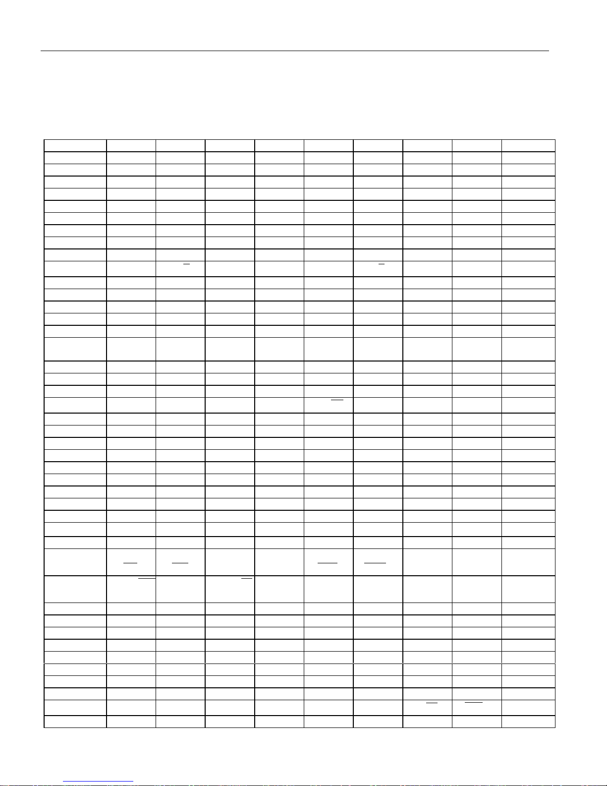
SPECIAL FUNCTION REGISTERS
The following table identifies the complete SFR map for the DS87C550.
DS87C550 SPECIAL FUNCTION REGISTER LOCATIONS : Table 550UG-1
REGISTER BIT 7 BIT 6 BIT 5 BIT 4 BIT 3 BIT 2 BIT 1 BIT 0 ADDRESS
P0 P0.7 P0.6 P0.5 P0.4 P0.3 P0.2 P0.1 P0.0 80h
SP 81h
DPL 82h
DPH 83h
DPL1 84h
DPH1 85h
DPS
PCON SMOD_0 SMOD0
TCON TF1 TR1 TF0 TR0 IE1 IT1 IE0 IT0 88h
TMOD GATE
TL0 8Ah
TL1 8Bh
TH0 8Ch
TH1 8Dh
CKCON WD1 WD0 T2M T1M T 0M MD2 MD1 MD0 8Eh
P1 P1.7
RCON
SCON0
SBUF0 99h
PMR
P2 P2.7 P2.6 P2.5 P2.4 P2.3 P2.2 P2.1 P2.0 A0
SADDR0
SADDR1
IE EA EAD ES1 ES0 ET1 EX1 ET0 EX0 A8h
CMPL0
CMPL1
CMPL2
CPTL0
CPTL1
CPTL2
CPTL3
P3 P3.7
ADCON1
ID1 ID0 TSL
OFDF OFDE
T/C
P1.6
TXD1
- - - - CKRDY RGMD RGSL BGS 91h
SM0/FE_0
CD1 CD0 SWB
RD
TRT
RXD1
SM1_0 SM2_0 REN_0 TB8_0 RB8_0 TI_0 RI_0 98h
P3.6
WR
BSY/
EOC
M1 M0 GATE
P1.5
T2EX
P3.5
T1
SS/CONT
- - - - SEL 86h
GF1 GF0 STOP IDLE 87h
T/C
P1.4
T2
CTM
P3.4
T0
ADEX WCQ WCM ADON WCIO
P1.3
INT5/CT3
X2/X4
P3.3
1INT
P1.2
INT4/CT2
ALEOFF DME1 DME0 9Fh
P3.2
0INT
M1 M0 89h
P1.1
INT3/CT1
P3.1
TXD0
P1.0
INT2/CT0
P3.0
RXD0
90h
A1h
A2h
A9h
AAh
ABh
ACh
ADh
AEh
AFh
B0h
B2h
ADCON2 OUTCF MUX2 MUX1 MUX0 APS3 APS2 APS1 APS0
ADMSB
ADLSB
WINHI
WINLO
IP SADEN0 B9h
SADEN1 BAh
T2CON
T2MOD
TF2 EXF2 RCLK TCLK EXEN2 TR2
- - - - - - T2OE DCEN BFh
PAD PS1
B3h
B4h
B5h
B6h
B7h
PS0 PT1 PX1 PT0 PX0 B8h
2T/C
2RL
BEh
5 of 93

DS87C550 High-Speed Microcontroller User’s Guide Supplement
REGISTER BIT 7 BIT 6 BIT 5 BIT 4 BIT 3 BIT 2 BIT 1 BIT 0 ADDRESS
P4 P4.7
CMT1
ROMSIZE - - - - - RMS2 RMS1 RMS0 C2h
STATUS
TA 1 1 1 1 1 1 1 1 C7h
T2IR - CM2F CM1F CM0F IE5/CF3 IE4/CF2 IE3/CF1 IE2/CF0
CMPH0
CMPH1
CMPH2
CPTH0
CPTH1
CPTH2
CPTH3
PSW CY AC F0 RS1 RS0 OV F1 P D0h
PW0FG
PW1FG
PW2FG
PW3FG
PWMADR ADRS - - - - - PWE1 PWE0
SCON1
SBUF1
PWM0
PWM1
PWM2
PWM3
ACC E0h
PW01CS PW0S2 PW0S1 PW0S0 PW0EN PW1S2 PW1S1 PW1S0 PW1EN
PW23CS PW2S2 PW2S1 PW2S0 PW2EN PW3S2 PW3S1 PW3S0 PW3EN
PW01CON PW0F PW0DC PW0OE PW0T/C PW1F PW1DC PW1OE PW1T/C
PW23CON PW2F PW2DC PW2OE PW2T/C PW3F PW3DC PW3OE PW3T/C
RLOADL
RLOADH
EIE ET2 ECM2 ECM1 ECM0 EX5/EC3 EX4/EC2 EX3/EC1 EX2/EC0 E8h
T2SEL TF2S TF2BS - TF2B - - T2P1 T2P0
CTCON
TL2
TH2
SETR TGFF1 TGFF0 CMS5 CMS4 CMS3 CMS2 CMS1 CMS0
RSTR CMT1 CMT0 CMR5 CMR4 CMR3 CMR2 CMR1 CMR0
B FOh
P6 P6.7 P6.6 P6.5 P6.4 P6.3 P6.2 P6.1 P6.0
EIP PT2 PCM2 PCM1 PCM0 PX5/PC3 PX4/PC2 PX3/PC1 PX2/PC0 F8h
WDCON SMOD_1 POR EPFI PFI WDIF WTRF EWT RWT
PIP HIP LIP - SPTA1 SPRA1 SPTA0 SPRA0 C5h
SM0/FE_1
P4.6
CMT0
SM1_1 SM2_1 REN_1 TB8_1 RB8_1 TI_1 RI_1
3CT
CT3
P4.5
CMSR5
2CT
P4.4
CMSR4
CT2
P4.3
CMSR3
1CT
P4.2
CMSR2
CT1
P4.1
CMSR1
0CT
P4.0
CMSR0
CT0
C0h
C8h
C9h
CAh
CBh
CCh
CDh
CEh
CFh
D2h
D3h
D4h
D5h
D6h
D8h
D9h
DCh
DDh
DEh
DFh
E1h
E2h
E3h
E4h
E6h
E7h
EAh
EBh
ECh
EDh
EEh
EFh
F1h
FFh
Note: Registers and bits in bold are new to the DS87C550. Registers and bits in bold AND Italic existed in
previous high-speed microcon tro ll ers, but at diffe ren t loca tions.
6 of 93

DS87C550 High-Speed Microcontroller User’s Guide Supplement
DS87C550 SPECIAL FUNCTION REGISTER RESET VALUES : Table 550UG-2
REGISTER BIT 7 BIT 6 BIT 5 BIT 4 BIT 3 BIT 2 BIT 1 BIT 0 ADDRESS
P0 1111111180h
SP 0000011181h
DPL 0000000082h
DPH 0000000083h
DPL1 0000000084h
DPH1 0 0 0 0 0 0 0 0 85h
DPS 0000010086h
PCON 0 0 Special 0 0 0 0 0 87h
TCON 0000000088h
TMOD 0000000089h
TL0 000000008Ah
TL1 000000008Bh
TH0 000000008Ch
TH1 000000008Dh
CKCON 000000018Eh
P1 1111111190h
RCON - - - - Special Special Special 0 91h
SCON0 0 0 0 0 0 0 0 0 98h
SBUF0 0000000099h
PMR 100000009Fh
P2 11111111A0
SADDR0 0 0 0 0 0 0 0 0 A1h
SADDR1 0 0 0 0 0 0 0 0 A2h
IE 00000000A8h
CMPL0 00000000A9h
CMPL1 00000000AAh
CMPL2 00000000ABh
CPTL0 0 0 0 0 0 0 0 0 ACh
CPTL1 00000000ADh
CPTL2 0 0 0 0 0 0 0 0 AEh
CPTL3 00000000AFh
P3 11111111B0h
ADCON1 0 0 0 0 0 0 0 0 B2h
ADCON2 0 0 0 0 0 0 0 0 B3h
ADMSB 00000000B4h
ADLSB 00000000B5h
WINHI 0 0 0 0 0 0 0 0 B6h
WINLO 00000000B7h
IP - 0 0 0 0 0 0 0 B8h
SADEN0 0 0 0 0 0 0 0 0 B9h
SADEN1 0 0 0 0 0 0 0 0 BAh
T2CON 00000000BEh
T2MOD ------00BFh
P4 11111111C0h
ROMSIZE00001100C2h
P5 11111111C4h
STATUS00010000C5h
TA 11111111C7h
T2IR - 0 0 0 0 0 0 0 C8h
CMPH0 00000000C9h
CMPH1 00000000CAh
CMPH2 00000000CBh
CPTH0 00000000CCh
CPTH1 00000000CDh
7 of 93

DS87C550 High-Speed Microcontroller User’s Guide Supplement
REGISTER BIT 7 BIT 6 BIT 5 BIT 4 BIT 3 BIT 2 BIT 1 BIT 0 ADDRESS
CPTH2 00000000CEh
CPTH3 00000000CFh
PSW 00000000D0h
PW0FG 0 0 0 0 0 0 0 0 D2h
PW1FG 0 0 0 0 0 0 0 0 D3h
PW2FG 0 0 0 0 0 0 0 0 D4h
PW3FG 0 0 0 0 0 0 0 0 D5h
PWMADR0 - ----00D6h
SCON1 0 0 0 0 0 0 0 0 D8h
SBUF1 00000000D9h
PWM0 00000000DCh
PWM1 00000000DDh
PWM2 00000000DEh
PWM3 00000000DFh
ACC 00000000E0h
PW01CS00000000E1h
PW23CS00000000E2h
PW01CON00000000E3h
PW23CON00000000E4h
RLOADL 0 0 0 0 0 0 0 0 E6h
RLOADH00000000E7h
EIE 00000000E8h
T2SEL 0 0 -0--00EAh
CTCON 0 0 0 0 0 0 0 0 EBh
TL2 00000000ECh
TH2 00000000EDh
SETR 1 10 0 0 0 0 0 EEh
RSTR 00000000EFh
B 00000000FOh
P6 1 - 1 1 1 1 1 1 F1h
EIP 00000000F8h
WDCON 0 Special 0 Special 0 Special Special 0 FFh
8 of 93

DS87C550 High-Speed Microcontroller User’s Guide Supplement
Port 0 (P0)
76543210
SFR 80h P0.7 P0.6 P0.5 P0.4 P0.3 P0.2 P0.1 P0.0
RW-1 RW-1 RW-1 RW-1 RW-1 RW-1 RW-1 RW-1
R=Unrestricted Read, W=Unrestricted Write, -n=Value after Reset
P0.7-0
Port 0. This port functions as a multiplexed address/data bus during external
memory access, and as a general purpose I/O port on devices with internal
program memory. During external memory cycles, this port drives the LSB of the
address when ALE is high, and data when ALE is low. When used as a general
purpose I/O, this port is open-drain and requires pull-ups. Writing a 1 to any pin
of this port places it in a high impedance mode, which is required if the pin is to
be used as an input. Pull-ups are not required when used as a memory interface.
Stack Pointer (SP)
76543210
SFR 81h SP.7 SP.6 SP.5 SP.4 SP.3 SP.2 SP.1 SP.0
RW-0 RW-0 RW-0 RW-0 RW-0 RW-1 RW-1 RW-1
R=Unrestricted Read, W=Unrestricted Write, -n=Value after Reset
SP.7-0
Bits 7-0
Stack Pointer. This stack pointer identifies the location where the stack will
begin. The stack pointer is incremented before every PUSH operation. This
register defaults to 07h after reset.
Data Pointer Low 0 (DPL)
76543210
SFR 82h DPL.7 DPL.6 DPL.5 DPL.4 DPL.3 DPL.2 DPL.1 DPL.0
RW-0 RW-0 RW-0 RW-0 RW-0 RW-0 RW-0 RW-0
R=Unrestricted Read, W=Unrestricted Write, -n=Value after Reset
DPL.7-0
Bits 7-0
Data Pointer Low 0. This register is the low byte of the standard 80C32 16-bit
data pointer. DPL and DPH are used to point to non-scratchpad data RAM.
Data Pointer High 0 (DPH)
76543210
SFR 83h DPH.7 DPH.6 DPH.5 DPH.4 DPH.3 DPH.2 DPH.1 DPH.0
RW-0 RW-0 RW-0 RW-0 RW-0 RW-0 RW-0 RW-0
R=Unrestricted Read, W=Unrestricted Write, -n=Value after Reset
DPH.7-0
Bits 7-0
Data Pointer High 0. This register is the high byte of the standard 80C32 16-bit
data pointer. DPL and DPH are used to point to non-scratchpad data RAM.
9 of 93

DS87C550 High-Speed Microcontroller User’s Guide Supplement
Data Pointer Low 1 (DPL1)
76543210
SFR 84h DPL1.7 DPL1.6 DPL1.5 DPL1.4 DPL1.3 DPL1.2 DPL1.1 DL1H.0
RW-0 RW-0 RW-0 RW-0 RW-0 RW-0 RW-0 RW-0
R=Unrestricted Read, W=Unrestricted Write, -n=Value after Reset
DPL1.7-0
Bits 7-0
Data Pointer Low 1. This register is the low byte of the auxiliary 16-bit data
pointer. When the SEL bit (DPS.0) is set, DPL1 and DPH1 are used in place of
DPL and DPH during DPTR operations.
Data Pointer High 1 (DPH1)
76543210
SFR 85h DPH1.7 DPH1.6 DPH1.5 DPH1.4 DPH1.3 DPH1.2 DPH1.1 DPH1.0
RW-0 RW-0 RW-0 RW-0 RW-0 RW-0 RW-0 RW-0
R=Unrestricted Read, W=Unrestricted Write, -n=Value after Reset
DPH1.7-0
Bits 7-0
Data Pointer High 1. This register is the high byte of the auxiliary 16-bit data
pointer. When the SEL bit (DPS.0) is set, DPL1 and DPH1 are used in place of
DPL and DPH during DPTR operations.
Data Pointer Select (DPS)
76543210
SFR 86hID1ID0TSL0----SEL
ID1, ID0
Bits 7-6
TSL
Bit 5
Bits 4-1
SEL
Bit 0
RW-0 RW-0 RW-0 R-0 R-0 R-0 R-0 RW-0
R=Unrestricted Read, W=Unrestricted Write, -n=Value after Reset
Increment/Decrement Select Bits These bits define how the INC DPTR
instruction functions in relation to the current DPTR as selected by SEL.
ID1 ID0 SEL = 0 SEL = 1
0 0 Increment DPTR Increment DPTR1
0 1 Decrement DPTR Increment DPTR1
1 0 Increment DPTR Decrement DPTR1
1 1 Decrement DPTR Decrement DPTR1
Toggle Select Bit Enable This bit allows any instruction involving the data
pointer to toggle the SEL bit automatically. When this bit is logic 1, the SEL
bit will automatically toggle, otherwise it will not.
Reserved. Read will be indeterminate.
Data Pointer Select. This bit selects the active data pointer.
0 = Instructions that use the DPTR will use DPL and DPH.
1= Instructions that use the DPTR will use DPL1 and DPH1.
10 of 93

DS87C550 High-Speed Microcontroller User’s Guide Supplement
Power Control (PCON)
76543210
SFR 87h SMOD_0 SMOD0 OFDF OFDE GF1 GF0 STOP IDLE
RW-0 RW-0 RW-* RW-0 RW-0 RW-0 RW-0 RW-0
R=Unrestricted Read, W=Unrestricted Write, -n=Value after Reset; *=see description
SMOD_0
Bit 7
SMOD0
Bit 6
OFDF
Bit 5
OFDE
Bit 4
Serial Port 0 Baud Rate Doubler Enable. This bit enables/disables the
serial baud rate doubling function for Serial Port 0.
0 = Serial Port 0 baud rate will be that defined by baud rate generation
equation.
1 = Serial Port 0 baud rate will be double that defined by baud rate generation
equation.
Framing Error Detection Enable. This bit selects function of the
SCON0.7 and SCON1.7 bits.
0 = SCON0.7 and SCON1.7 control the SM0 function defined for the
SCON0 and SCON1 registers.
1 = SCON0.7 and SCON1.7 are converted to the Framing Error (FE) flag for
the respective Serial Port.
Oscillator Fail Detect Flag. This bit is set if a reset is caused by oscillator
failure and must be cleared by software.
Oscillator Fail Detect Enable. This bit enables the oscillator fail detect circuitry
when 1 and disables the feature when 0.
GF1
Bit 3
GF0
Bit 2
STOP
Bit 1
IDLE
Bit 0
General Purpose User Flag 1. This is a general purpose flag for software
control.
General Purpose User Flag 0. This is a general purpose flag for software
control.
Stop Mode Select. Setting this bit will stop program execution, halt the CPU
oscillator and internal timers, and place the CPU in a low-power mode. This bit
will always be read as a 0. Setting this bit while the Idle bit is set will place the
device in an undefined state.
Idle Mode Select. Setting this bit will stop program execution but leave the CPU
oscillator, timers, serial ports, and interrupts active. This bit will always be read
as a 0.
11 of 93

DS87C550 High-Speed Microcontroller User’s Guide Supplement
Timer/Counter Control (TCON)
76543210
SFR 88h TF1 TR1 TF0 TR0 IE1 IT1 IE0 IT0
RW-0 RW-0 RW-0 RW-0 RW-0 RW-0 RW-0 RW-0
R=Unrestricted Read, W=Unrestricted Write, -n=Value after Reset
TF1
Bit 7
TR1
Bit 6
TF0
Bit 5
TR0
Bit 4
Timer 1 Overflow Flag. This bit indicates when Timer 1 overflows its
maximum count as defined by the current mode. This bit can be cleared by
software and is automatically cleared when the CPU vectors to the Timer 1
interrupt service routine.
0 = No Timer 1 overflow has been detected.
1 = Timer 1 has overflowed its maximum count.
Timer 1 Run Control. This bit enables/disables the operation of Timer 1.
0 = Timer 1 is halted.
1 = Timer 1 is enabled.
Timer 0 Overflow Flag. This bit indicates when Timer 0 overflows its
maximum count as defined by the current mode. This bit can be cleared by
software and is automatically cleared when the CPU vectors to the Timer 0
interrupt service routine or by software.
0 = No Timer 0 overflow has been detected.
1 = Timer 0 has overflowed its maximum count.
Timer 0 Run Control. This bit enables/disables the operation of Timer 0.
Halting this timer will preserve the current count in THO and TL0.
0 = Timer 0 is halted.
1 = Timer 0 is enabled.
IE1
Bit 3
IT1
Bit 2
IE0
Bit 1
IT0
Bit 0
Interrupt 1 Edge Detect. This bit is set when an edge/level of the type defined
by IT1 is detected. If IT1=1, this bit will remain set until cleared in software or
the start of the External Interrupt 1 service routine. If IT1=0, this bit will
inversely reflect the state of the INT1 pin.
Interrupt 1 Type Select. This bit selects whether the
INT1pin will detect edge
or level triggered interrupts.
0 = INT1 is level triggered.
1 = INT1 is edge triggered.
Interrupt 0 Edge Detect. This bit is set when an edge/level of the type defined
by IT0 is detected. If IT0=1, this bit will remain set until cleared in software or
the start of the External Interrupt 0 service routine. If IT0=0, this bit will
inversely reflect the state of the 0INT pin
Interrupt 0 Type Select. This bit selects whether the
0INT pin will detect edge
or level triggered interrupts.
0 =
0INT is level triggered.
1 = 0INT is edge triggered.
12 of 93

Timer Mode Control (TMOD)
76543210
DS87C550 High-Speed Microcontroller User’s Guide Supplement
SFR 89h GATE
RW-0 RW-0 RW-0 RW-0 RW-0 RW-0 RW-0 RW-0
R=Unrestricted Read, W=Unrestricted Write, -n=Value after Reset
GATE
Bit 7
T/C
Bit 6
M1, M0
Bits 5-4
T/C
M1 M0 GATE
T/C
M1 M0
Timer 1 Gate Control. This bit enable/disables the ability of Timer 1 to
increment.
0 = Timer 1 will clock when TR1=1, regardless of the state of
INT1.
1 = Timer 1 will clock only when TR1=1 and INT1=1.
Timer 1 Counter/Timer Select.
0 = Timer 1 is incremented by internal clocks (timer).
1 = Timer 1 is incremented by pulses on T1 when TR1 (TCON.6) is 1 (counter).
Timer 1 Mode Select. These bits select the operating mode of Timer 1.
M1 M0 Mode
0 0 Mode 0: 8 bit with 5-bit prescale
0 1 Mode 1: 16 bit with no prescale.
1 0 Mode 2: 8 bit with auto-reload
1 1 Mode 3: Timer 1 is halted, but holds its count.
GATE
Bit 3
T/C
Bit 2
M1, M0
Bits 1-0
Timer 0 Gate Control. This bit enables/disables that ability of Timer 0 to
increment.
0 = Timer 0 will clock when TR0=1, regardless of the state of 0INT .
1 = Timer 0 will clock only when TR0=1 and 0INT = 1.
Timer 0 Counter/Timer Select.
0 = Timer incremented by internal clocks (timer).
1 = Timer 1 is incremented by pulses on T0 when TR0 (TCON.4) is 1 (counter).
Timer 0 Mode Select. These bits select the operating mode of Timer 0.
When Timer 0 is in mode 3, TL0 is started/stopped by TR0 and TH0 is
started/stopped by TR1. Run control for Timer 1 is then provided via the
Timer 1 mode selection.
M1 M0 Mode
0 0 Mode 0: 8 bit with 5-bit prescale
0 1 Mode 1: 16 bit no prescale
1 0 Mode 2: 8 bit with auto-reload
1 1 Mode 3: Timer 0 is two 8 bit counters.
13 of 93

DS87C550 High-Speed Microcontroller User’s Guide Supplement
Timer 0 LSB (TL0)
76543210
SFR 8Ah TL0.7 TL0.6 TL0.5 TL0.4 TL0.3 TL0.2 TL0.1 TL0.0
RW-0 RW-0 RW-0 RW-0 RW-0 RW-0 RW-0 RW-0
R=Unrestricted Read, W=Unrestricted Write, -n=Value after Reset
TL0.7-0
Bits 7-0
Timer 0 LSB. This register contains the least significant byte of Timer 0.
Timer 1 LSB (TL1)
76543210
SFR 8Bh TL1.7 TL1.6 TL1.5 TL1.4 TL1.3 TL1.2 TL1.1 TL1.0
RW-0 RW-0 RW-0 RW-0 RW-0 RW-0 RW-0 RW-0
R=Unrestricted Read, W=Unrestricted Write, -n=Value after Reset
TL1.7-0
Bits 7-0
Timer 1 LSB. This register contains the least significant byte of Timer 1.
Timer 0 MSB (TH0)
76543210
SFR 8Ch TH0.7 TH0.6 TH0.5 TH0.4 TH0.3 TH0.2 TH0.1 TH0.0
RW-0 RW-0 RW-0 RW-0 RW-0 RW-0 RW-0 RW-0
R=Unrestricted Read, W=Unrestricted Write, -n=Value after Reset
TH0.7-0
Bits 7-0
Timer 0 MSB. This register contains the most significant byte of Timer 0.
Timer 1 MSB (TH1)
76543210
SFR 8Dh TH1.7 TH1.6 TH1.5 TH1.4 TH1.3 TH1.2 TH1.1 TH1.0
RW-0 RW-0 RW-0 RW-0 RW-0 RW-0 RW-0 RW-0
R=Unrestricted Read, W=Unrestricted Write, -n=Value after Reset
TH1.7-0
Bits 7-0
Timer 1 MSB. This register contains the most significant byte of Timer 1.
14 of 93
DS87C550 High-Speed Microcontroller User’s Guide Supplement
Clock Control (CKCON)
76543210
SFR 8Eh WD1 WD0 T2M T1M T0M MD2 MD1 MD0
RW-0 RW-0 RW-0 RW-0 RW-0 RW-0 RW-0 RW-1
R=Unrestricted Read, W=Unrestricted Write, -n=Value after Reset
WD1, WD0
Bits 7-6
T2M
Bit 5
Watchdog Timer Mode Select 1-0. These bits determine the watchdog timer
time-out period. The timer divides the crystal (or external oscillator) frequency
by a programmable value as shown below. The divider value is expressed in
crystal (oscillator) cycles. The settings of the system clock control bits X2/X4
(PMR.3) and CD1:0 (PMR.7-6) will affect the clock input to the watchdog
timer and therefore its time-out period as shown below. All Watchdog Timer
reset time-outs follow the setting of the interrupt flag by 512 clocks. The
DS87C550 does not incorporate a watchdog interrupt, but a similar effect may
be achieved by polling its flag.
Watchdog Interrupt Flag Time-Out Periods (in crystal clocks)
CD1:0 WD1:0=00 WD1:0=01 WD1:0=10 WD1:0=11
X2/X4
100 2
000 2
X01 2
X10 2
X11 2
15
16
17
17
25
18
2
19
2
20
2
20
2
28
2
21
2
22
2
23
2
23
2
31
2
24
2
25
2
26
2
26
2
34
2
Timer 2 Clock Select. This bit controls the division of the system clock that
drives Timer 2. This bit has no effect when the timer is in baud rate generator or
clock output modes. Clearing this bit to 0 maintains 80C32 compatibility. This
bit has no effect on instruction cycle timing.
T1M
Bit 4
T0M
Bit 3
0 = Timer 2 uses a divide by 12 of the crystal frequency.
1 = The divide ratio of Timer 2 is determined by the CD1, CD0, and 4X/
X2 as
shown below.
Timer 1 Clock Select. This bit controls the division of the system clock that
drives Timer 1. Clearing this bit to 0 maintains 80C32 compatibility. This bit
has no effect on instruction cycle timing.
0 = Timer 1 uses a divide by 12 of the crystal frequency.
1 = The divide ratio of Timer 1 is determined by the CD1, CD0, and 4X/
X2 as
shown below.
Timer 0 Clock Select. This bit controls the division of the system clock that
drives Timer 0. Clearing this bit to 0 maintains 80C32 compatibility. This bit
has no effect on instruction cycle timing.
0 = Timer 0 uses a divide by 12 of the crystal frequency.
1 = The divide ratio of Timer 0 is determined by the CD1, CD0, and 4X/
X2 as
shown below.
15 of 93

DS87C550 High-Speed Microcontroller User’s Guide Supplement
Timer 0, 1, and 2 values as a function of various clock control settings
OSCILLATOR
CYCLES PER
MACHINE.
CD1:0
4X/2X
00 1 1 12 1 2 3 1 64 32
00 0 2 12 2 2 6 2 64 32
01 x Reserved
10 x 4 12 4 2 12 4 64 32
11 x 1024 3072 1024 512 3072 1024 64 32
MD2, MD1, MD0
Bits 2-0
CYCLE
Stretch MOVX Select 2-0. These bits select the time by which external MOVX
cycles are to be stretched. This allows slower memory or peripherals to be
OSC CYCLES
PER TIMER 0/1/2
CLOCK.
TxM=0 TxM=1
OSC CYCLES
PER TIMER 2
CLK, BAUD
RATE GEN.
OSC CYCLES PER
SERIAL PORT CLK,
MODE 0
SM2=0 SM2=1 SMOD=0 SMOD=1
OSC CYCLES PER
SERIAL PORT CLK,
MODE 2
accessed without using ports or manual software intervention. The RD or
WR strobe will be stretched by the specified interval, which will be transparent to
the software except for the increased time to execute to MOVX instruction. All
internal MOVX instructions on devices containing MOVX SRAM are performed
at the 2 machine cycle rate.
MD2 MD1 MD0 Stretch Value MOVX Duration
0 0 0 0 2 Machine Cycles
0 0 1 1 3 Machine Cycles (reset default)
0 1 0 2 4 Machine Cycles
0 1 1 3 5 Machine Cycles
1 0 0 4 9 Machine Cycles
1 0 1 5 10 Machine Cycles
1 1 0 6 11 Machine Cycles
1 1 1 7 12 Machine Cycles
16 of 93

Port 1 (P1)
DS87C550 High-Speed Microcontroller User’s Guide Supplement
76543210
SFR 90h
P1.7-0
Bits 7-0
TXD1
Bit 7
RXD1
Bit 6
T2EX
Bit 5
P1.7
TXD1
P1.6
RXD1
P1.5
T2EX
P1.4
T2
P1.3
P1.2
3CT/5INT
2CT/4INT
P1.1
1CT/3INT
RW-1 RW-1 RW-1 RW-1 RW-1 RW-1 RW-1 RW-1
R=Unrestricted Read, W=Unrestricted Write, -n=Value after Reset
General Purpose I/O Port 1. This register functions as a general purpose I/O
port. In addition, all the pins have an alternative function listed below. P1.2-7
contain functions that are new to the 80C32 architecture. The Timer 2 functions
on pins P1.1-0 are available on the 80C32, but not the 80C31. Each of the
functions is controlled by several other SFRs. The associated Port 1 latch bit
must contain a logic one before the pin can be used in its alternate function
capacity.
Serial Port 1 Transmit. This pin transmits the serial port 1 data in serial port
modes 1, 2, 3 and emits the synchronizing clock in serial port mode 0.
Serial Port 1 Receive. This pin receives the serial port 1 data in serial port
modes 1, 2, 3 and is a bi-directional data transfer pin in serial port mode 0.
Timer 2 Capture/Reload Trigger. A 1 to 0 transition on this pin will cause the
value in the T2 registers to be transferred into the capture registers if enabled by
EXEN2 (T2CON.3). When in auto–reload mode, a 1 to 0 transition on this pin
will reload the timer 2 registers with the value in RCAP2L and RCAP2H if
enabled by EXEN2 (T2CON.3).
P1.0
0CT/2INT
T2
Bit 4
Bit 3
Bit 2
Bit 1
Bit 0
Timer 2 External Input. A 1 to 0 transition on this pin will cause timer 2
increment or decrement depending on the timer configuration. This mode of
operation is enabled by setting the 2T/C bit (T2CON.1).
3CT/5INT
External Interrupt 5/Capture 3 Input. In normal operation, a falling edge on
this pin will cause an external interrupt 5 (if enabled). If capture channel 3 is
enabled, this pin acts as a capture command input.
2CT/4INT
External Interrupt 4/Capture 2 Input. In normal operation, a falling edge on
this pin will cause an external interrupt 4 (if enabled). If capture channel 2 is
enabled, this pin acts as a capture command input.
1CT/3INT
External Interrupt 3/Capture 1 Input. In normal operation, a falling edge on
this pin will cause an external interrupt 3 (if enabled). If capture channel 1 is
enabled, this pin acts as a capture command input.
0CT/2INT
External Interrupt 2/Capture 0 Input. In normal operation, a falling edge on
this pin will cause an external interrupt 2 (if enabled). If capture channel 0 is
enabled, this pin acts as a capture command input.
17 of 93

DS87C550 High-Speed Microcontroller User’s Guide Supplement
Ring Oscillator Control (RCON)
76543210
SFR 91h - - - - CKRDY RGMD RGSL BGS
R-* R-* RW-* RT-0
R=Unrestricted Read, W=Unrestricted Write, T=Timed Access Write Only, -n =Value after
Reset, * = See Description
Bits 7 – 4 Reserved. Read data will be indeterminate.
CKRDY
Bit 3
RGMD
Bit 2
RGSL
Bit 1
Clock Ready This bit indicates the status of the start-up period delay used to
establish the crystal oscillator or crystal multiplier warm-up period of 65536
crystal oscillator periods. A 1 indicates that the period is complete otherwise it is
not. This bit is cleared after a reset or when exiting STOP mode. It is also cleared
when the clock multiplier is enabled (CTM bit of the PMR register set). Once the
CKRDY bit is set, the lockout preventing CD1:CD0 from being modified is
removed, and clock multiplier may then be selected as the clock source.
Ring Oscillator Mode This bit indicates the status of the ring oscillator. If 0, the
ring is not being used, and if 1, the system is running from the ring. This bit must
be cleared before the RGSL can be modified, before the Clock Control divider
bits (CD1:CD0) can be changed to any condition other than divide by 4 mode,
and before enabling the clock multiplier (setting the CTM bit).
Ring Oscillator Select This bit enables (1) or disables (0) the ring oscillator. If
enabled, the ring oscillator will be used as the system clock source after exiting
STOP mode until the end of start-up period delay (65536 crystal oscillator
periods). At the end of this delay, the crystal oscillator will automatically be
switched in as the system clock source. This bit is reset only by a Power-On
Reset.
BGS
Bit 0
Band Gap Select This bit enables (1) or disables (0) the band-gap voltage
reference in STOP mode.
18 of 93

DS87C550 High-Speed Microcontroller User’s Guide Supplement
Serial Port 0 Control (SCON0)
76543210
SFR 98h SM0/FE_0 SM1_0 SM2_0 REN_0 TB8_0 RB8_0 T1_0 R1_0
RW-0 RW-0 RW-0 RW-0 RW-0 RW-0 RW-0 RW-0
R=Unrestricted Read, W=Unrestricted Write, -n=Value after Reset
SM0-2
Bits 7-5
Serial Port Mode These bits control the mode of serial port 0. In addition the
SM0 and SM2_0 bits have secondary functions as shown below.
SM0 SM1 SM2 MODE FUNCTION LENGTH PERIOD
0 0 0 0 Synchronous 8 bits 12 t
0 0 1 0 Synchronous 8 bits 4 t
CLK
CLK
0 1 X 1 Asynchronous 10 bits Timer 1 or 2 baud rate equation
1 0 0 2 Asynchronous 11 bits 64 t
32 t
1 0 1 1 Asynchronous w/
Multiprocessor
communication
11 bits 64 t
32 t
(SMOD=0)
CLK
(SMOD=1)
CLK
(SMOD=0)
CLK
(SMOD=1)
CLK
1 1 0 3 Asynchronous 11 bits Timer 1 or 2 baud rate equation
1 1 1 3 Asynchronous w/
11 bits Timer 1 or 2 baud rate equation
Multiprocessor
communication
SM0/FE_0
Bit 7
SM1_0
Bit 6
SM2_0
Bit 5
Framing Error Flag. When SMOD0 (PCON.6)=0, this bit (SM0) is used to
select the mode for serial port 0. When SMOD0=1, this bit (FE) will be set upon
detection of an invalid stop bit. When used as FE, this bit must be cleared in
software. Once the SMOD0 bit is set, modifications to this bit will not affect the
serial port mode settings. Although accessed from the same register, internally the
data for bits SM0 and FE are stored in different locations.
No alternate function.
Multiple CPU Communications. The function of this bit is dependent on the
serial port 0 mode.
Mode 0: Selects 12 t
CLK
or 4 t
period for synchronous serial port 0 data
CLK
transfers.
Mode 1: When set, reception is ignored (RI_0 is not set) if invalid stop bit
received.
Mode 2/3: When this bit is set, multiprocessor communications are enabled in
modes 2 and 3. This will prevent the RI_0 bit from being set, and an
interrupt being asserted, if the 9
th
bit received is not 1.
19 of 93

DS87C550 High-Speed Microcontroller User’s Guide Supplement
REN_0
Bit 4
TB8_0
Bit 3
RB8_0
Bit 2
TI_0
Bit 1
RI_0
Bit 0
Receiver Enable. This bit enable/disables the serial port 0 receiver shift register.
0 = Serial port 0 reception disabled.
1= Serial port 0 receiver enabled (modes 1, 2, 3). Setting this bit will initiate
synchronous reception in mode 0.
9th Transmission Bit State. This bit defines the state of the 9th transmission bit
in serial port 0 modes 2 and 3.
9th Received Bit State. This bit identifies that state of the 9th reception bit of
received data in serial port 0 modes 2 and 3. In serial port mode 1, when
SM2_0=0, RB8_0 is the state of the stop bit. RB8_0 is not used in mode 0.
Transmitter Interrupt Flag. This bit indicates that data in the serial port 0
buffer has been completely shifted out. In serial port mode 0, TI_0 is set at the
end of the 8th data bit. In all other modes, this bit is set at the end of the last data
bit. This bit must be manually cleared by software.
Receiver Interrupt Flag. This bit indicates that a byte of data has been received
in the serial port 0 buffer. In serial port mode 0, RI_0 is set at the end of the 8
th
bit. In serial port mode 1, RI_0 is set after the last sample of the incoming stop bit
subject to the state of SM2_0. In modes 2 and 3, RI_0 is set after the last sample
of RB8_0. This bit must be manually cleared by software.
Serial Data Buffer 0 (SBUF0)
76543210
SFR 99h SBUF0.7 SBUF0.6 SBUF0.5 SBUF0.4 SBUF0.3 SBUF0.2 SBUF0.1 SBUF0.0
RW-0 RW-0 RW-0 RW-0 RW-0 RW-0 RW-0 RW-0
R=Unrestricted Read, W=Unrestricted Write, -n=Value after Reset
SBUF0.7-0
Bits 7-0
Serial Data Buffer 0. Data for serial port 0 is read from or written to this
location. The serial transmit and receive buffers are separate registers, but both
are addressed at this location.
20 of 93

DS87C550 High-Speed Microcontroller User’s Guide Supplement
Power Management Register (PMR)
76543210
SFR 9Fh CD1 CD0 SWB CTM
R*-1 R*-0 RW-0 R*-0 R*-0 RW-0 RW-0 RW-0
R=Unrestricted Read, W=Unrestricted Write, -n=Value after Reset; * = See Description
CD1,CD0
Bits 7, 6
Clock Divide Control : These bits select the source of the system clock and
determine the number of clocks per machine cycle as indicated in the table.
CD1 CD0 Clock source; divisor
00Crystal multiplier; 1 or 2 clocks per machine cycle (as determined
by the
X2/X4 bit.
01Reserved.
10Crystal/external oscillator; 4 clocks per machine cycle (default)
11Crystal/external oscillator; 1024 clocks per machine cycle.
A default of 10b is selected after all forms of reset and Stop mode exits. When
changing these bits certain restrictions must be observed. The default state is the
only state that any other state can be changed to or from. As an example,
attempting to change from the crystal multiplier clock source (either divide by 1
or 2) directly to the crystal/external oscillator divided by 1024 will result in CD1
and CD0 remaining unchanged.
ALEOFF DME1 DME0
X2/X4
SWB
Bit 5
CTM
Bit 4
Bit 3
Switch Back Enable This bit enables (1) or disables (0) the switch-back
function. When enabled, switchback will allow the processor to automatically
switch from divide by 1024 mode to divide by 4 mode when an external interrupt
is acknowledged or when a start bit of a serial character is recognized on an
active serial port.
Crystal Multiplier Enable This bit enables (1) or disables (0) the crystal
multiplier function. By clearing this bit, the power required by this circuitry can
be saved. Setting this bit will automatically clear the CKRDY bit and initiate the
start-up period delay. Until the start-up period has elapsed, CKRDY will remain
cleared and it will be impossible to change the CD1 & CD0 bits to select the
crystal multiplier. Also, CTM cannot be changed unless CD1 & CD0 = 10b and
RGMD is cleared to 0. This bit is automatically cleared to 0 when the processor
enters Stop mode.
X2/X4
Clock Multiplier Selection This bit selects the clock multiplication factor as
shown.
X2/X4 = 0 Sets the frequency multiplier to 2 times the incoming clock.
X2/X4 = 1 Sets the frequency multiplier to 4 times the incoming clock.
This bit can only be altered when the Crystal Multiplier Enable bit (CTM) is
cleared. Therefore it must be set for the desired multiplication factor prior to
setting the CTM bit.
21 of 93

ALEOFF
Bit 2
DS87C550 High-Speed Microcontroller User’s Guide Supplement
ALE Disable When set to 1, this bit disables ALE during on-board memory
accesses. Any off-chip memory access will cause ALE to automatically toggle
regardless of the state of this bit. When this bit is 0, ALE toggles for all memory
accesses whether the memory is inside or outside of the chip.
DME1,DME0
Bits 1, 0
DME1 DME0 Data Memory Range Memory Access
0 0 0000h – FFFFh External data memory (default)
0 1 0000h – 03FFh 1K Internal SRAM data memory
0400h – FFFFh External data memory
1 0 Reserved Reserved
1 0 0000h – 3FFFh 1K Internal SRAM data memory
0400h – FFFBh Reserved.
FFFCh System control byte (EPROM
Read-Only).
FFFDh – FFFF Reserved.
Port 2 (P2)
76543210
SFR A0h P2.7 P2.6 P2.5 P2.4 P2.3 P2.2 P2.1 P2.0
RW-1 RW-1 RW-1 RW-1 RW-1 RW-1 RW-1 RW-1
R=Unrestricted Read, W=Unrestricted Write, -n=Value after Reset
P2.7-0
Bits 7-0
Port 2. This port functions as an address bus during external memory access, and
as a general purpose I/O port on devices which incorporate internal program
memory. During external memory cycles, this port will contain the MSB of the
address. The Port 2 latch does not control general purpose I/O pins on ROMLESS
devices, but is still used to hold the address MSB during register-indirect data
memory operations such as MOVX A, @R1.
Slave Address Register 0 (SADDR0)
76543210
SFR A1h
SADDR0.7-0
Bits 7-0
SADDR0.7 SADDR0.6 SADDR0.5 SADDR0.4 SADDR0.3 SADDR0.2 SADDR0.1 SADDR0.0
RW-0 RW-0 RW-0 RW-0 RW-0 RW-0 RW-0 RW-0
R=Unrestricted Read, W=Unrestricted Write, -n=Value after Reset
Slave Address Register 0. This register is programmed by the user with the
given or broadcast address assigned to serial port 0.
22 of 93

DS87C550 High-Speed Microcontroller User’s Guide Supplement
Slave Address Register 1 (SADDR1)
76543210
SFR A2h
SADDR1.7 SADDR1.6 SADDR1.5 SADDR1.4 SADDR1.3 SADDR1.2 SADDR1.1 SADDR1.0
RW-0 RW-0 RW-0 RW-0 RW-0 RW-0 RW-0 RW-0
R=Unrestricted Read, W=Unrestricted Write, -n=Value after Reset
SADDR1.7-0
Bits 7-0
Slave Address Register 1. This register is programmed by the user with the
given or broadcast address assigned to serial port 1.
Interrupt Enable (IE)
76543210
SFR A8h EA EAD ES1 ES0 ET1 EX1 ET0 EX0
RW-0 RW-0 RW-0 RW-0 RW-0 RW-0 RW-0 RW-0
R=Unrestricted Read, W=Unrestricted Write, -n=Value after Reset
EA
Bit 7
EAD
Bit 6
Global Interrupt Enable. This bit controls the global masking of all interrupts
except Power-Fail Interrupt, which is enabled by the EPFI bit (WDCON.5).
0 = Disable all interrupt sources. This bit overrides individual interrupt mask
settings.
1 = Enable all individual interrupt masks. Individual interrupts will occur if
enabled.
A/D Interrupt Enable. This bit controls the masking of the A/D Converter
interrupt.
0 = Disable the A/D interrupt.
ES1
Bit 5
ES0
Bit 4
ET1
Bit 3
1 = Enable interrupt requests generated by the EOC (ADCON.6) flag.
Enable Serial Port 1 Interrupt. This bit controls the masking of the Serial Port
1 interrupt.
0 = Disable all Serial Port 1 interrupts.
1 = Enable interrupt requests generated by the RI_1 (SCON1.0) or TI_1
(SCON1.1) flags.
Enable Serial Port 0 Interrupt. This bit controls the masking of the Serial port
0 interrupt.
0 = Disable all serial port 0 interrupts.
1 = Enable interrupt requests generated by the RI_0 (SCON0.0) or TI_0
(SCON0.1) flags.
Enable Timer 1 Interrupt. This bit controls the masking of the Timer 1
interrupt.
0 = Disable all Timer 1 interrupts.
1 = Enable all interrupt requests generated by the TF1 flag (TCON.7).
23 of 93

DS87C550 High-Speed Microcontroller User’s Guide Supplement
EX1
Bit 2
Enable External Interrupt 1. This bit controls the masking of external interrupt
1.
0 = Disable external interrupt 1.
1 = Enable all interrupt requests generated by the 1INT pin.
ET0
Bit 1
Enable Timer 0 Interrupt. This bit controls the masking of the Timer 0
interrupt.
0 = Disable all Timer 0 interrupts.
1 = Enable all interrupt requests generated by the TF0 flag (TCON.5).
EX0
Bit 0
Enable External Interrupt 0. This bit controls the masking of external interrupt
0.
0 = Disable external interrupt 0.
1 = Enable all interrupt requests generated by the 0INT pin.
Compare Register Zero LSB (CMPL0)
76543210
SFR A9h
CMPL0.7 CMPL0.6 CMPL0.5 CMPL0.4 CMPL0.3 CMPL0.2 CMPL0.1 CMPL0.0
RW-0 RW-0 RW-0 RW-0 RW-0 RW-0 RW-0 RW-0
R=Unrestricted Read, W=Unrestricted Write, -n=Value after Reset
CMPL0.7-0
Bits 7-0
Compare Register Zero LSB. This register is one of three used to store the least
significant 8-bit value for the Timer 2’s comparison functions. When a match
occurs between Timer 2 and the contents of 16-bit register pair made of CMPH0
& CMPL0, port pins P4.5 through P4.0 are set if the corresponding compare
match set enable bits (CMS5:0=SETR.5:0) are set.
Compare Register One LSB (CMPL1)
76543210
SFR AAh
CMPL1.7-0
Bits 7-0
CMPL1.7 CMPL1.6 CMPL1.5 CMPL1.4 CMPL1.3 CMPL1.2 CMPL1.1 CMPL1.0
RW-0 RW-0 RW-0 RW-0 RW-0 RW-0 RW-0 RW-0
R=Unrestricted Read, W=Unrestricted Write, -n=Value after Reset
Compare Register One LSB. This register is one of three used to store the least
significant 8-bit value for the Timer 2’s comparison functions. When a match
occurs between Timer 2 and the contents of 16-bit register pair made of CMPH1
& CMPL1, port pins P4.5 through P4.0 are reset if the corresponding compare
match reset enable bits (CMR5:0=RSTR.5:0) are set.
24 of 93

DS87C550 High-Speed Microcontroller User’s Guide Supplement
Compare Register Two LSB (CMPL2)
76543210
SFR ABh
CMPL2.7 CMPL2.6 CMPL2.5 CMPL2.4 CMPL2.3 CMPL2.2 CMPL2.1 CMPL2.0
RW-0 RW-0 RW-0 RW-0 RW-0 RW-0 RW-0 RW-0
R=Unrestricted Read, W=Unrestricted Write, -n=Value after Reset
CMPL2.7-0
Bits 7-0
Compare Register Two LSB. This register is one of three used to store the least
significant 8-bit value for the Timer 2’s comparison functions. When a match
occurs between Timer 2 and the contents of 16-bit register pair made of CMPH2
& CMPL2, port pin P4.6 will toggle if the corresponding compare match toggle
enable bit CMTE0 (RSTR.6) is set. Similarly on a match, P4.7 will toggle if the
corresponding compare match toggle enable bit CMTE1 (RSTR.7) is set.
Capture Register Zero LSB (CPTL0)
76543210
SFR ACh CPTL0.7 CPTL0.6 CPTL0.5 CPTL0.4 CPTL0.3 CPTL0.2 CPTL0.1 CPTL0.0
RW-0 RW-0 RW-0 RW-0 RW-0 RW-0 RW-0 RW-0
R=Unrestricted Read, W=Unrestricted Write, -n=Value after Reset
CPTL0.7-0
Bits 7-0
Capture Register Zero LSB. This register is used to capture the least significant
8-bit value for the Timer 2’s channel 0 capture function. When a transition
occurs on the INT2/CT0 pin, the LSB of Timer 2 is captured in this register on
the rising edge if the CT0=CTCON.0 enable bit is set or on the falling edge if the
0CT =CTCON.1 enable is set. Setting both enable bits will cause a capture to
occur on both edges.
Capture Register One LSB (CPTL1)
76543210
SFR ADh CPTL1.7 CPTL1.6 CPTL1.5 CPTL1.4 CPTL1.3 CPTL1.2 CPTL1.1 CPTL1.0
RW-0 RW-0 RW-0 RW-0 RW-0 RW-0 RW-0 RW-0
R=Unrestricted Read, W=Unrestricted Write, -n=Value after Reset
CPTL1.7-0
Bits 7-0
Capture Register One LSB. This register is used to capture the least significant
8-bit value for the Timer 2’s channel 1 capture function. When a transition
occurs on the INT3/CT1 pin, the LSB of Timer 2 is captured in this register on
the rising edge if the CT1=CTCON.1 enable bit is set or on the falling edge if the
1CT =CTCON.3 enable is set. Setting both enable bits will cause a capture to
occur on both edges.
25 of 93

DS87C550 High-Speed Microcontroller User’s Guide Supplement
Capture Register Two LSB (CPTL2)
76543210
SFR AEh CPTL2.7 CPTL2.6 CPTL2.5 CPTL2.4 CPTL2.3 CPTL2.2 CPTL2.1 CPTL2.0
RW-0 RW-0 RW-0 RW-0 RW-0 RW-0 RW-0 RW-0
R=Unrestricted Read, W=Unrestricted Write, -n=Value after Reset
CPTL2.7-0
Bits 7-0
Capture Register Two LSB. This register is used to capture the least significant
8-bit value for the Timer 2’s channel 2 capture function. When a transition
occurs on the INT4/CT2 pin, the LSB of Timer 2 is captured in this register on
the rising edge if the CT2=CTCON.4 enable bit is set or on the falling edge if the
2CT =CTCON.5 enable is set. Setting both enable bits will cause a capture to
occur on both edges.
Capture Register Three LSB (CPTL3)
76543210
SFR AFh CPTL3.7 CPTL3.6 CPTL3.5 CPTL3.4 CPTL3.3 CPTL3.2 CPTL3.1 CPTL3.0
RW-0 RW-0 RW-0 RW-0 RW-0 RW-0 RW-0 RW-0
R=Unrestricted Read, W=Unrestricted Write, -n=Value after Reset
CPTL3.7-0
Bits 7-0
Capture Register Three LSB. This register is used to capture the least
significant 8-bit value for the Timer 2’s channel 3 capture function. When a
transition occurs on the INT5/CT3 pin, the LSB of Timer 2 is captured in this
register on the rising edge if the CT3=CTCON.6 enable bit is set or on the falling
edge if the 3CT =CTCON.7 enable is set. Setting both enable bits will cause a
capture to occur on both edges.
26 of 93

Port 3 (P3)
DS87C550 High-Speed Microcontroller User’s Guide Supplement
76543210
SFR B0h P3.7
RD
RW-1 RW-1 RW-1 RW-1 RW-1 RW-1 RW-1 RW-1
R=Unrestricted Read, W=Unrestricted Write, -n=Value after Reset
P3.7-0
Bits 7-0
RD
Bit 7
WR
Bit 6
T1
Bit 5
P3.6
WR
P3.5
T1
P3.4
T0
P3.3
P3.2
1INT
0INT
P3.1
TXD0
P3.0
RXD0
General Purpose I/O Port 3. This register functions as a general purpose I/O
port. In addition, all the pins have an alternative function listed below. Each of
the functions is controlled by several other SFRs. The associated Port 3 latch bit
must contain a logic one before the pin can be used in its alternate function
capacity.
External Data Memory Read Strobe. This pin provides an active low read
strobe to an external memory or peripheral device.
External Data Memory Write Strobe. This pin provides an active low write
strobe to an external memory or peripheral device.
Timer/Counter External Input. A 1 to 0 transition on this pin will increment
Timer 1 if counter mode is enabled.
T0
Bit 4
1INT
Bit 3
0INT
Bit 2
TXD0
Bit 1
RXD0
Bit 0
Timer/Counter External Input. A 1 to 0 transition on this pin will increment
Timer 0 if counter mode is enabled.
External Interrupt 1. A falling edge/low level on this pin will cause an external
interrupt 1 if enabled.
External Interrupt 0. A falling edge/low level on this pin will cause an external
interrupt 0 if enabled.
Serial Port 0 Transmit. This pin transmits the serial port 0 data in serial port
modes 1, 2, 3 and emits the synchronizing clock in serial port mode 0.
Serial Port 0 Receive. This pin receives the serial port 0 data in serial port
modes 1, 2, 3 and is a bi-directional data transfer pin in serial port mode 0.
27 of 93

DS87C550 High-Speed Microcontroller User’s Guide Supplement
A/D Converter Control Register 1 (ADCON1)
76543210
SFR B2h
BSY/STRT
Bit 7
EOC
Bit 6
Bit 5
ADEX
Bit 4
BSY/STRT
EOC
SS/CONT
ADEX WCQ WCM ADON WCIO
R*-0 RW-0 RW-0 RW-0 RW-0 R-0 RW-0 RW-0
R=Unrestricted Read, W=Unrestricted Write, -n=Value after Reset; *=See description
Start/Busy. When this bit is changed from a 0 to a 1, an A/D conversion starts. It
remains set for the duration of the conversion process (regardless of attempts to
write 0). Hardware automatically clears this bit upon completion of conversion.
End Of Conversion. This bit is set by hardware when a conversion is complete.
It also serves as an interrupt flag qualified by WCQ and enabled by EAD (IE.7).
This bit must be cleared by software and can be set or cleared by software
anytime.
SS/CONT
Continuous/Single Shot. When set to 1, the A/D converter operates in
continuous mode and repeatedly runs conversions once a conversion is initiated.
When this bit is cleared, the A/D converter performs one conversion and stops.
A/D External Start. When set, this bit allows an A/D conversion to be initiated
by the detection of a falling edge on the STADC pin.
WCQ
Bit 3
WCM
Bit 2
ADON
Bit 1
WCIO
Bit 0
Window Comparator Qualifier. If set, this bit allows an A/D converter
interrupt to occur only when both EOC and WCM bits are set at the end of a
conversion. If this bit is cleared, an interrupt will occur (if enabled) every time
EOC is set.
Window Comparator Match. This bit is set by hardware at the end of an A/D
conversion result that matches the criteria set by WINHI, WINLO, and WCIO.
This bit is not set if there is no match, and it must be cleared by software.
A/D On. This bit enables (ADON=1) or disables (ADON=0) the A/D function.
Changing this bit from a 0 to a 1 requires a warm-up period of 4 µs before a
proper conversion can be performed. This bit can be cleared to save power when
no conversion is required, and clearing it aborts any conversion in progress. This
action also resets the BSY/STRT bit.
Window Compare Inside/Outside. When set to 1, the window comparison
function looks for A/D results that are outside of the window bounded by the
limits set by WINHI and WINLO. When this bit is cleared, the check is for values
inside these limits.
28 of 93
 Loading...