

Dallas DS80C390 User Manual
r
Dual CAN High-Speed Microprocesso
www.maxim-ic.com
GENERAL DESCRIPTION
The DS80C390 is a fast 8051-compatible
microprocessor with dual CAN 2.0B controllers. The
redesigned processor core executes 8051
instructions up to 3X faster than the original for the
same crystal speed. The DS80C390 supports a
maximum crystal speed of 40MHz, resulting in
apparent execution speeds of 100MHz
(approximately 2.5X). An optional internal frequency
multiplier allows the microprocessor to operate at full
speed with a reduced crystal frequency, reducing
EMI. A hardware math accelerator further increases
the speed of 32-bit and 16-bit multiply and divide
operations as well as high-speed shift, normalization,
and accumulate functions.
The High-Speed Microcontroller User’s Guide and High-Speed
Microcontroller User’s Guide: DS80C390 Supplement must be
used in conjunction with this data sheet. Download both at:
www.maxim-ic.com/microcontrollers
.
APPLICATIONS
Industrial Controls Agricultural Equipment
Factory Automation Gaming Equipment
Medical Equipment
Automotive
Heating, Ventilation, and
Air Conditioning
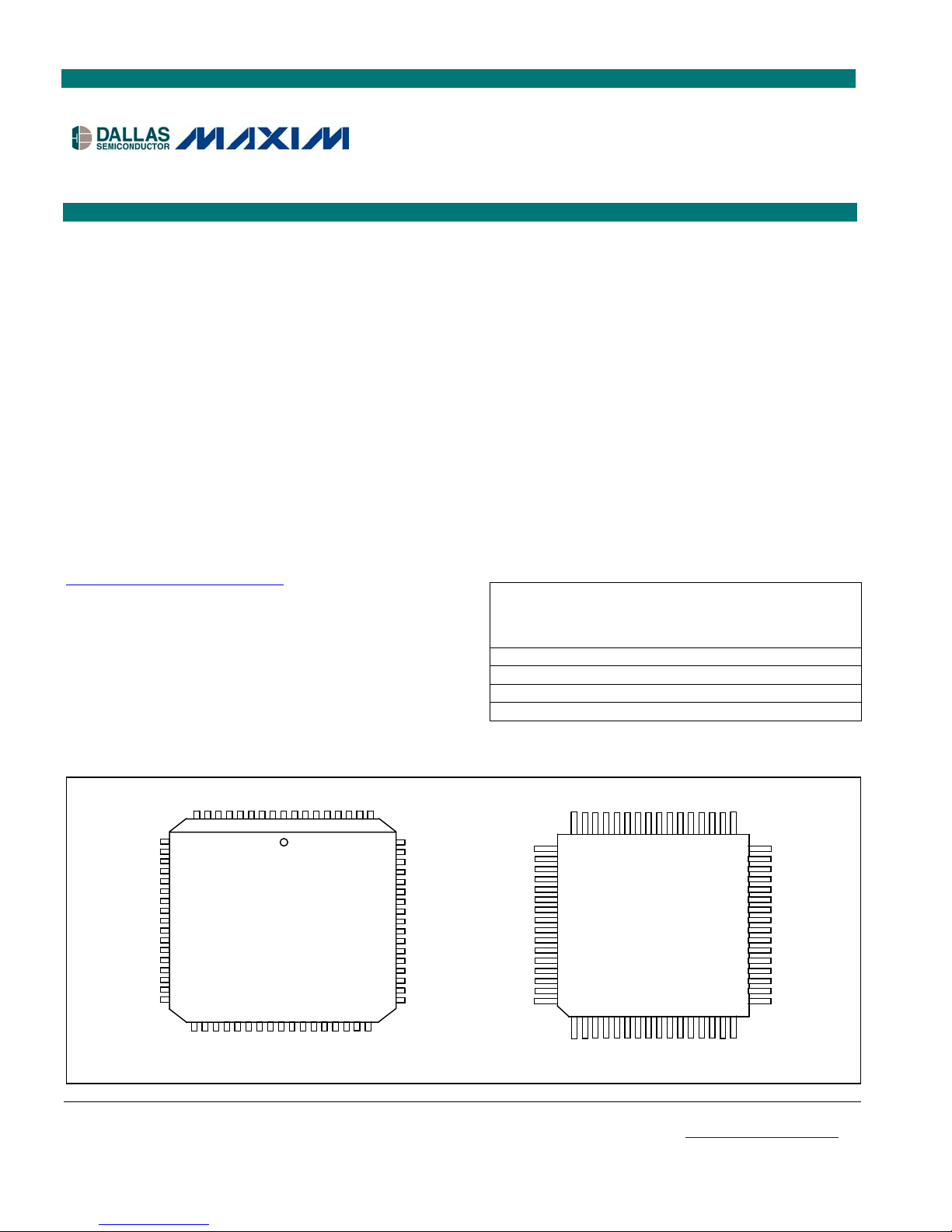
PIN CONFIGURATIONS
DS80C390
FEATURES
§ 80C52 Compatible
§ High-Speed Architecture
§ 4kB Internal SRAM Usable as Program/
Data/Stack Memory
§ Enhanced Memory Architecture
§ Two Full-Function CAN 2.0B Controllers
§ Two Full-Duplex Hardware Serial Ports
§ Programmable IrDA Clock
§ High Integration Controller
§ 16 Interrupt Sources with Six External
§ Available in 64-Pin LQFP, 68-Pin PLCC
See page 29 for a complete list of features.
ORDERING INFORMATION
MAX
PART TEMP RANGE
DS80C390-QCR 0°C to +70°C
DS80C390-QNR -40°C to +85°C
DS80C390-FCR 0°C to +70°C
DS80C390-FNR -40°C to +85°C
CLOCK
SPEED
(MHz)
40
40
40
40
PINPACKAGE
68 PLCC
68 PLCC
64 LQFP
64 LQFP
TOP VIEW
Dallas Semiconductor
DS80C390
PLCC
Note: Some revisions of this device may incorporate deviations from published specifications known as errata. Multiple revisions of any device
may be simultaneously available through various sales channels. For information about device errata, click here: www.maxim-ic.com/errata
1 of 54
48 33
49
Dallas Semiconductor
32
DS80C390
64
17
16 1
LQFP
.
REV: 022305

DS80C390 Dual CAN High-Speed Microprocessor
ABSOLUTE MAXIMUM RATINGS
Voltage Range on Any Pin Relative to Ground……………………………………………………….-0.3V to (VCC + 0.5V)
Voltage Range on V
Relative to Ground……………………………………………………………………-0.3V to +6.0V
CC
Operating Temperature Range………………………………………………………………………………..-40°C to +85°C
Storage Temperature Range………………………………………………………………………………...-55°C to +125°C
Soldering Temperature…..……………………………………………………………………..See IPC/JEDEC J-STD-020
Stresses beyond those listed under “Absolute Maximum Ratings” may cause permanent damage to the device. These are stress ratings only,
and functional operation of the device at these or any other conditions beyond those indicated in the operational sections of the specifications is
not implied. Exposure to the absolute maximum rating conditions for extended periods may affect device reliability.
DC ELECTRICAL CHARACTERISTICS (Note 10)
PARAMETER SYMBOL MIN TYP MAX UNITS
Supply Voltage VCC V
Power-Fail Warning V
Minimum Operating Voltage V
4.10 4.38 4.60 V
PFW
3.85 4.13 4.35 V
RST
Supply Current, Active Mode (Note 1) ICC 80 150 mA
Supply Current, Idle Mode (Note 2) I
Supply Current, Stop Mode (Note 3) I
Supply Current, Stop Mode, Bandgap Enabled (Note 3) I
40 75 mA
IDLE
1 120
STOP
150 350
SPBG
Input Low Level VIL -0.5 +0.8 V
Input High Level VIH 2.0 VCC +0.5 V
Input High Level for XTAL1, RST V
Output Low Voltage for Port 1, 3, 4, 5 at IOL = 1.6mA V
Output Low Voltage for Port 0, 1, 2, 4, 5, RD, WR, RSTOL, PSEN,
and ALE at I
= 3.2mA (Note 5)
OL
Output High Voltage for Port 1, 3, 4, 5 at IOH = -50mA (Note 4)
Output High Voltage for Port 1, 3, 4, 5 at IOH = -1.5mA (Note 6) V
Output High Voltage for Port 0, 1, 2, 4, 5, RD, WR, RSTOL, PSEN,
and ALE at I
= -8mA (Note 5, 7)
OH
0.7 x VCC VCC +0.5 V
IH2
0.45 V
OL1
V
0.45 V
OL2
2.4 V
V
OH1
2.4 V
OH2
V
2.4 V
OH3
Input Low Current for Port 1, 3, 4, 5 at 0.45V (Note 8) IIL -55
Logic 1 to 0 Transition Current for Port 1, 3, 4, 5 (Note 9) IT1 -650
Input Leakage Current for Port 0 (Input Mode Only) IL -300 +300
RST Pulldown Resistance R
50 170
RST
Note 1:
Note 2:
Note 3:
Note 4:
Note 5:
Note 6:
Note 7:
Note 8:
Note 9:
Note 10:
Active current measured with 40MHz clock source on XTAL1, V
Idle mode current measured with 40MHz clock source on XTAL1, V
Stop mode current measured with XTAL1 = RST = EA = V
RST = V
Applies to port pins when they are used to address external memory or as CAN interface signals.
This measurement reflects the port during a 0-to-1 transition in I/O mode. During this period a one-shot circuit drives the ports hard
for two clock cycles. If a port 4 or 5 pin is functioning in memory mode with pin state of 0 and the SFR bit contains a 1, changing
the pin to an I/O mode (by writing to P4CNT) will not enable the 2-cycle strong pullup. During Stop or Idle mode the pins switch to
I/O mode, and so port 2 and port 1 (in nonmultiplexed mode) will not exhibit the 2-cycle strong pullup when entering Stop or Idle
mode.
Port 3 pins 3.6 and 3.7 have a stronger than normal pullup drive for one oscillator period following the transition of either the RD or
WR from a 0-to-1 transition.
This is the current required from an external circuit to hold a logic low level on an I/O pin while the corresponding port latch bit is
set to 1. This is only the current required to hold the low level; transitions from 1 to 0 on an I/O pin also have to overcome the
transition current.
Ports 1(in I/O mode), 3, 4, and 5 source transition current when being pulled down externally. It reaches its maximum at
approximately 2V.
Specifications to -40°C are guaranteed by design and not production tested.
. This condition mimics operation of pins in I/O mode.
CC
= RST = 5.5V, all other pins disconnected.
CC
= 5.5V, RST = EA = VSS, all other pins disconnected.
CC
, VCC = 5.5V, all other pins disconnected.
SS
5.0 5.5 V
RST
mA
mA
mA
mA
mA
kW
2 of 54
DS80C390 Dual CAN High-Speed Microprocessor
AC ELECTRICAL CHARACTERISTICS—(MULTIPLEXED ADDRESS/DATA BUS)
(Note 10, Note 11)
PARAMETER SYMBOL CONDITIONS
Oscillator Frequency 1 / t
ALE Pulse Width t
Port 0 Instruction Address or CE0–4
Valid to ALE Low
External oscillator 0 40 0 40
LHLL
t
AVLL
CLCL
External crystal 1 40 1 40
0.125 t
40MHz VARIABLE CLOCK
MIN MAX MIN MAX
0.375 t
MCS
- 5
- 5 ns
MCS
ns
UNITS
MHz
Address Hold After ALE Low t
ALE Low to Valid Instruction In t
ALE Low to PSEN Low
PSEN Pulse Width
PSEN Low to Valid Instruction In
Input Instruction Hold After PSEN
Input Instruction Float After PSEN
Port 0 Address to Valid Instruction In t
Port 2, 4 Address to Valid Instruction
In
PSEN Low to Address Float
Note 11:
All parameters apply to both commercial and industrial temperature operation unless otherwise noted. The value t
of the machine cycle clock in terms of the processor’s input clock frequency. These relationships are described in the Stretch Value
Timing table. All signals characterized with load capacitance of 80pF except Port 0, ALE, PSEN, RD, and WR with 100pF.
Interfacing to memory devices with float times (turn off times) over 25ns can cause bus contention. This does not damage the
parts, but causes an increase in operating current. Specifications assume a 50% duty cycle for the oscillator. Port 2 and ALE timing
changes in relation to duty cycle variation. Some AC timing characteristic drawings contain references to the CLK signal. This
waveform is provided to assist in determining the relative occurrence of events and cannot be used to determine the timing of
signals relative to the external clock. AC timing is characterized and guaranteed by design but is not production tested.
0.125 t
LLAX1
0.625 t
LLIV
t
0.125 t
LLPL
t
0.5 t
PLPH
t
0.5 t
PLIV
t
0 0 ns
PXIX
t
0.25 t
PXIZ
0.75 t
AVIV1
t
0.875 t
AVIV2
t
0 0 ns
PLAZ
- 5 ns
MCS
- 20 ns
MCS
- 5 ns
MCS
- 8 ns
MCS
- 20 ns
MCS
- 5 ns
MCS
- 22 ns
MCS
- 30 ns
MCS
MCS
is a function
3 of 54

DS80C390 Dual CAN High-Speed Microprocessor
AC SYMBOLS
The DS80C390 uses timing parameters and symbols similar to the original 8051 family. The following list of timing
symbols is provided as an aid to understanding the timing diagrams.
SYMBOL FUNCTION
t Time
A Address
C Clock
CE Chip Enable
D Input Data
H Logic Level High
L Logic Level Low
I Instruction
P
Q Output Data
R
V Valid
W
X No longer a valid logic level.
Z Tri-State
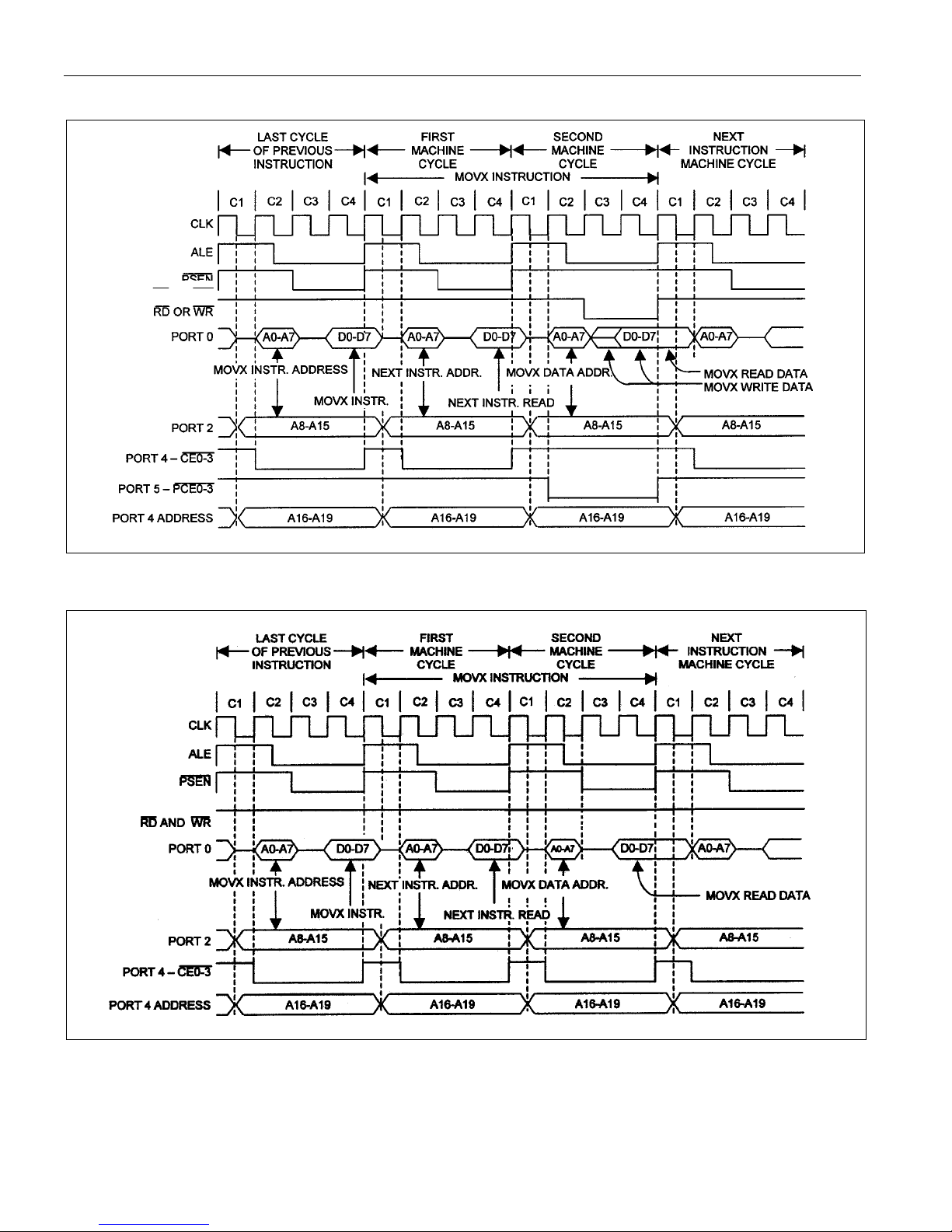
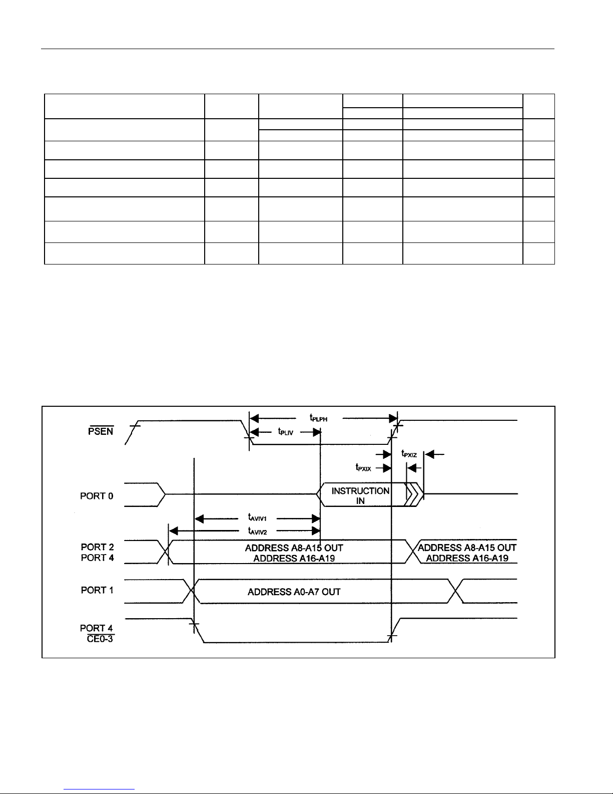
Figure 1. Multiplexed External Program Memory Read Cycle
PSEN
RD Signal
WR Signal
4 of 54

DS80C390 Dual CAN High-Speed Microprocessor
MOVX CHARACTERISTICS (MULTIPLEXED ADDRESS/DATA BUS) (Note 12)
PARAMETER SYMBOL MIN MAX UNITS
C
MOVX ALE Pulse Width t
Port 0 MOVX Address, CE0–4,
PCE0–4 Valid to ALE Low
Address Hold After MOVX
Read/Write
RD Pulse Width
WR Pulse Width
RD Low to Valid Data In
Data Hold After Read t
Data Float After Read t
ALE Low to Valid Data In t
Port 0 Address, Port 4 CE, Port 5
PCE to Valid Data In
Port 2, 4 Address to Valid Data In t
ALE Low to RD or WR Low
Port 0 Address, Port 4 CE, Port 5
PCE to RD or WR Low
Port 2, 4 Address to or WR Low
Data Valid to WR Transition
Data Hold After WR High
RD Low to Address Float
RD or WR High to ALE, Port 4 CE
or Port 5 PCE High
Note 12:
All parameters apply to both commercial and industrial temperature operation. CST is the stretch cycle value determined by the
MD2:0 bits. t
except Port 0, ALE, PSEN, RD, and WR with 100pF. Interfacing to memory devices with float times over 25ns can cause bus
contention and an increase in operating current. Specifications assume a 50% duty cycle for the oscillator; port 2 and ALE timing
changes in relation to duty cycle variation. Some AC timing characteristic drawings show the CLK signal, provided to determine the
relative occurrence of events and not the timing of signals relative to the external clock. During the external addressing mode, weak
latches maintain the previously driven value from the processor on Port 0 until Port 0 is overdriven by external memory; and on Port
1, 2 and 4 for one XTAL1 cycle prior to change in output address from Port 1, 2, and 4.
is a time period shown in the t
MCS
0.375 t
LHLL2
0.5 t
1.5 t
0.125 t
t
AVLL2
0.25t
1.25 t
t
LLAX2
t
LLAX3
t
RLRH
t
WLWH
t
RLDV
0 ns
RHDX
RHDZ
LLDV
t
AVDV1
AVDV2
0.25t
0.125 t
1.25 t
0.5 t
C
ST
0.5 t
C
ST
0.125 t
t
LLWL
0.25t
1.25 t
0.25 t
t
AVWL1
0.5t
2.5 t
0.375 t
t
AVWL2
0.625t
2.625 t
t
-8 ns
QVWX
0.25 t
t
WHQX
0.5t
1.5 t
t
RLAZ
t
WHLH
0.25 t
1.25 t
Time Periods table. All signals characterized with load capacitance of 80pF
MCS
- 5 ns CST = 0
MCS
- 5 ns
MCS
- 10 ns
MCS
- 5 ns CST = 0
MCS
- 5 ns
MCS
- 10 ns
MCS
-5 ns CST = 0
MCS
- 5 ns
MCS
- 5 ns
MCS
- 6 ns CST = 0
MCS
x t
- 10 ns
MCS
- 6 ns CST = 0
MCS
x t
- 10 ns
MCS
0.5 t
C
ST
0.25 t
0.5t
1.5 t
0.625 t
(CST + 0.25) x t
(C
+ 1.25) x t
ST
0.75 t
(4CST + 0.5) x t
(4C
+ 2.5) x t
ST
0.75 t
(4CST + 0.5) x t
(4CST + 2.5) x t
- 5 0.125 t
MCS
- 5 0.25t
MCS
- 5 1.25 t
MCS
- 11 ns CST = 0
MCS
- 11 ns
MCS
- 11 ns
MCS
- 11 ns CST = 0
MCS
- 11 ns
MCS
- 11 ns
MCS
- 8 ns CST = 0
MCS
- 10 ns
MCS
- 10 ns
MCS
See Note 12
- 20 ns CST = 0
MCS
x t
- 25 ns
MCS
- 5 ns CST = 0
MCS
- 5
MCS
- 5
MCS
- 20 ns CST = 0
MCS
- 20 ns
MCS
- 20 ns
MCS
- 26 ns CST = 0
MCS
- 30 ns
MCS
- 30 ns
MCS
- 30 ns CST = 0
MCS
- 30 ns
MCS
- 30 ns
MCS
+ 10 ns CST =0
MCS
+ 10 ns
MCS
+ 10 ns
MCS
ns
ns
-5 +10 ns CST = 0
- 7 0.25 t
MCS
- 7 1.25 t
MCS
+ 5 ns
MCS
+10 ns
MCS
STRETCH
VALUES
(MD2:0)
ST
£ 3
1 £ C
ST
£ 7
4 £ C
ST
£ 3
1£ C
ST
£ 7
4 £ C
ST
£ 3
1£ C
ST
£ 7
4 £ C
ST
£ 7
1 £ C
ST
£ 7
1 £ C
ST
£ 7
1 £ C
ST
£ 3
1 £ C
ST
£ 7
4 £ C
ST
£ 3
1 £ C
ST
£ 7
4 £ C
ST
£ 3
1£ C
ST
£ 7
4 £ C
ST
£ 3
1 £ C
ST
£ 7
4 £ C
ST
£ 3
1 £ C
ST
£ 7
4 £ C
ST
£ 3
1 £ C
ST
£ 7
4 £ C
ST
£ 3
1 £ C
ST
£ 7
4 £ C
ST
£ 3
1 £ C
ST
£ 7
4 £ C
ST
£ 3
1 £ C
ST
£ 7
4 £ C
ST
5 of 54

DS80C390 Dual CAN High-Speed Microprocessor
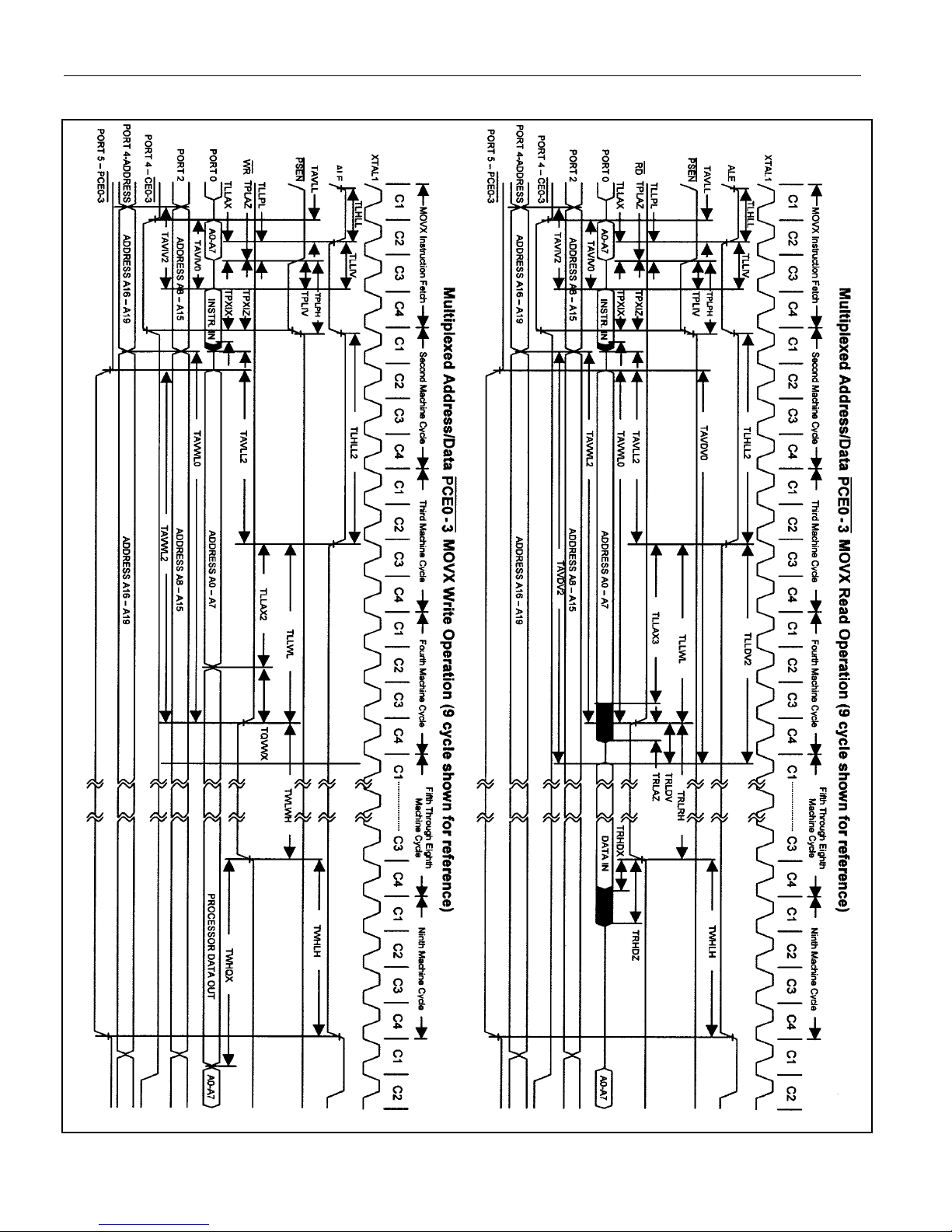
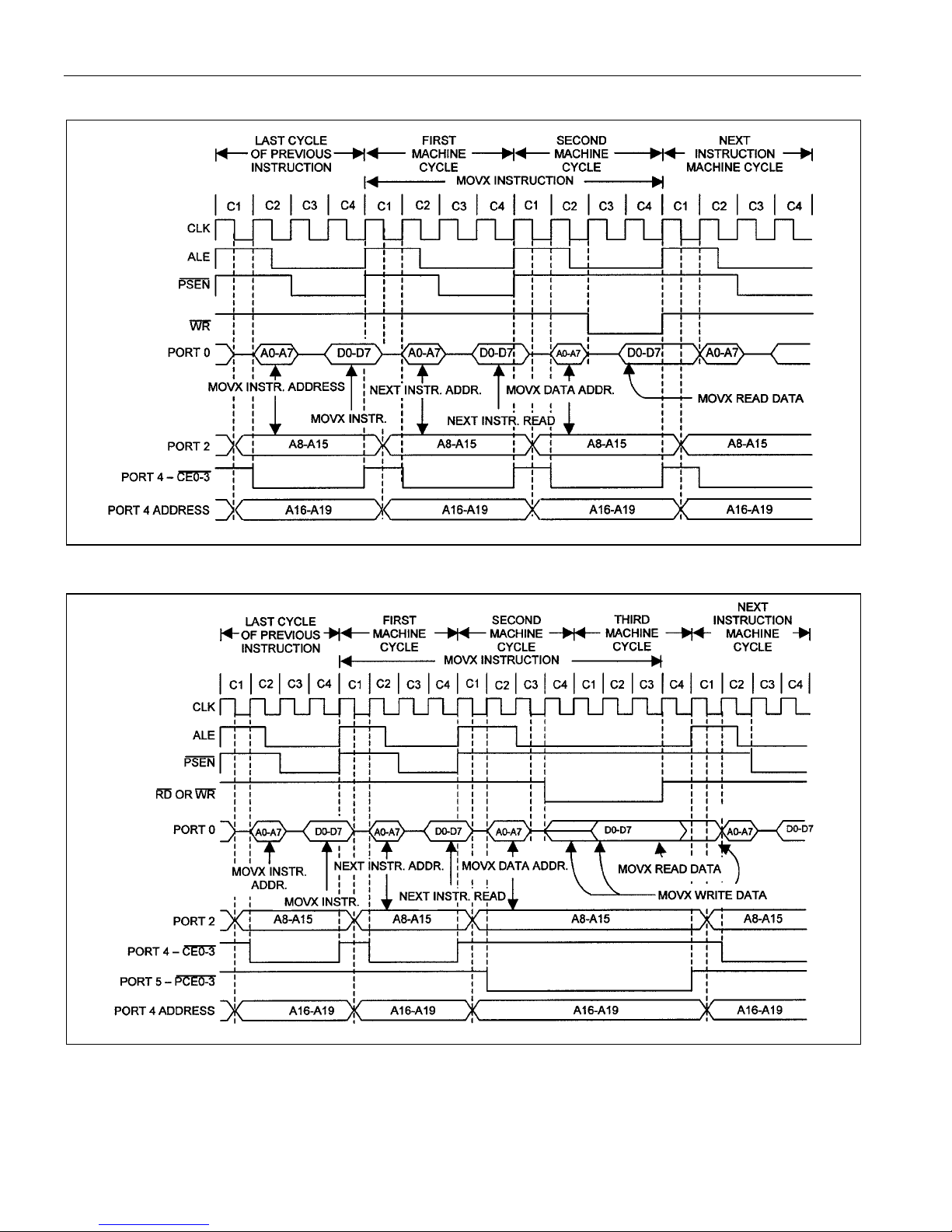
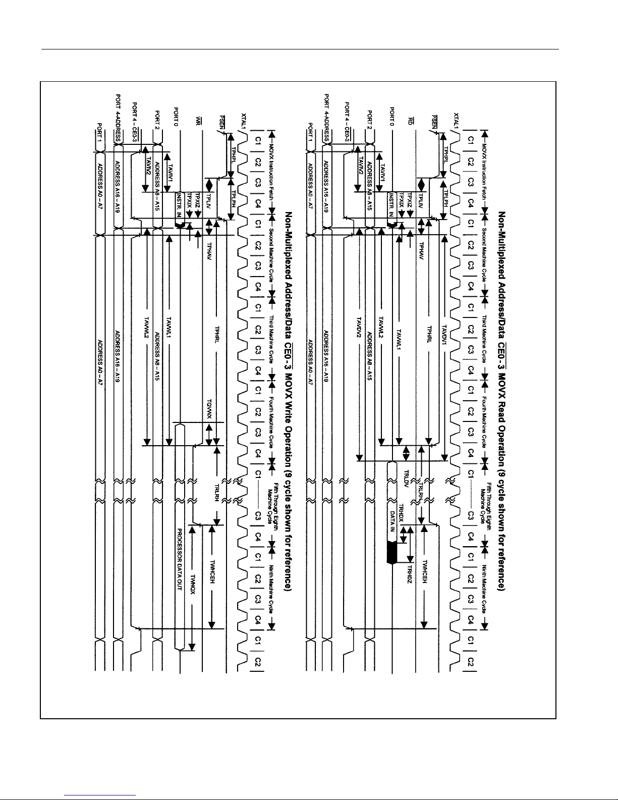
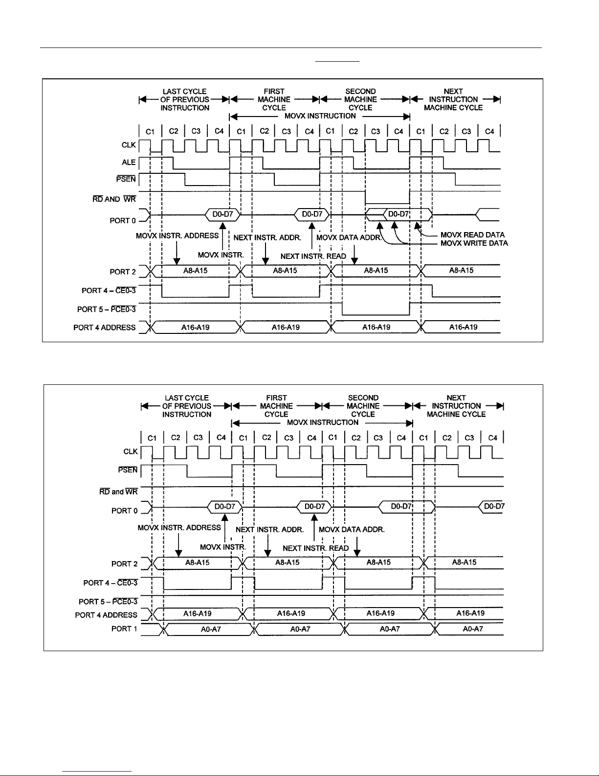
Figure 2. Multiplexed 9-Cycle Address/Data CE0-3 MOVX Read/Write Operation
6 of 54
DS80C390 Dual CAN High-Speed Microprocessor
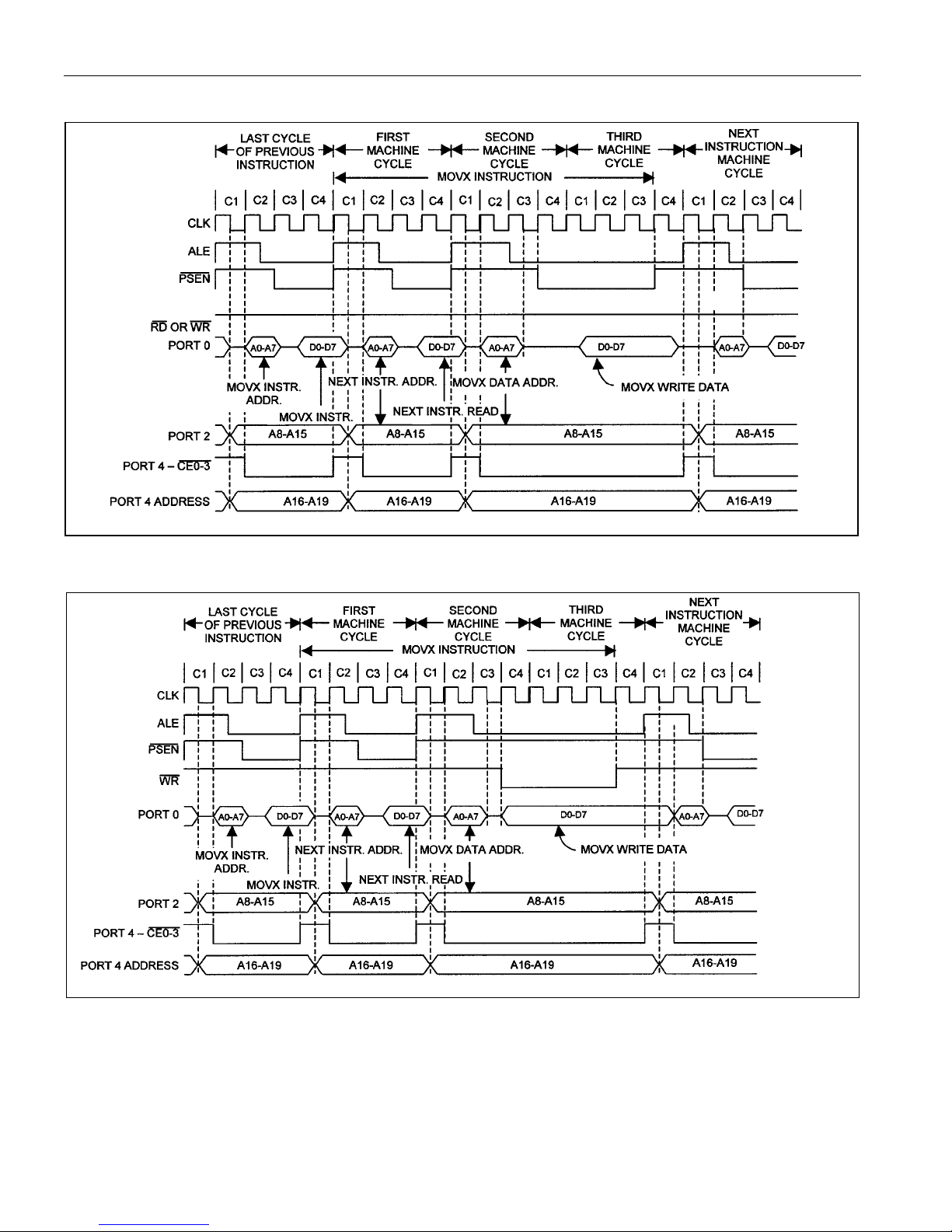
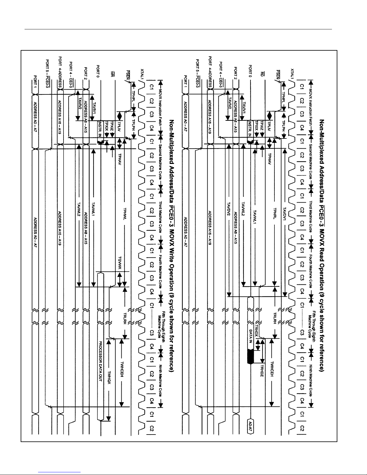
Figure 3. Multiplexed 9-Cycle Address/Data PCE0-3 MOVX Read/Write Operation
7 of 54
DS80C390 Dual CAN High-Speed Microprocessor
Figure 4. Multiplexed 2-Cycle Data Memory PCE0-3 Read or Write
Figure 5. Multiplexed 2-Cycle Data Memory CE0-3 Read
8 of 54
DS80C390 Dual CAN High-Speed Microprocessor
Figure 6. Multiplexed 2-Cycle Data Memory CE0-3 Write
Figure 7. Multiplexed 3-Cycle Data Memory PCE0-3 Read or Write
9 of 54
DS80C390 Dual CAN High-Speed Microprocessor
Figure 8. Multiplexed 3-Cycle Data Memory CE0-3 Read
Figure 9. Multiplexed 3-Cycle Data Memory CE0-3 Write
10 of 54
DS80C390 Dual CAN High-Speed Microprocessor
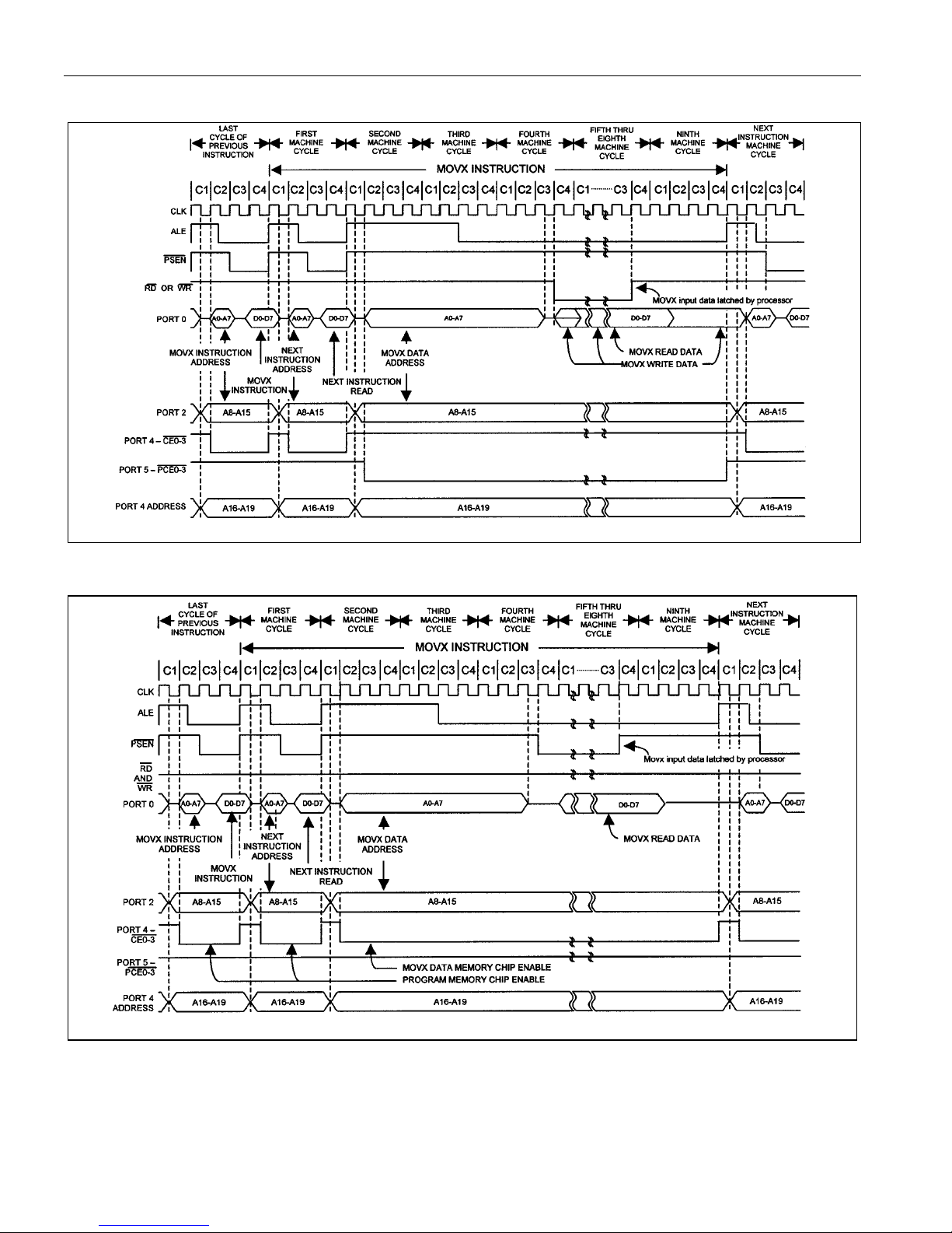
Figure 10. Multiplexed 9-Cycle Data Memory PEC0-3 Read or Write
Figure 11. Multiplexed 9-Cycle Data Memory CE0-3 Read
11 of 54
DS80C390 Dual CAN High-Speed Microprocessor
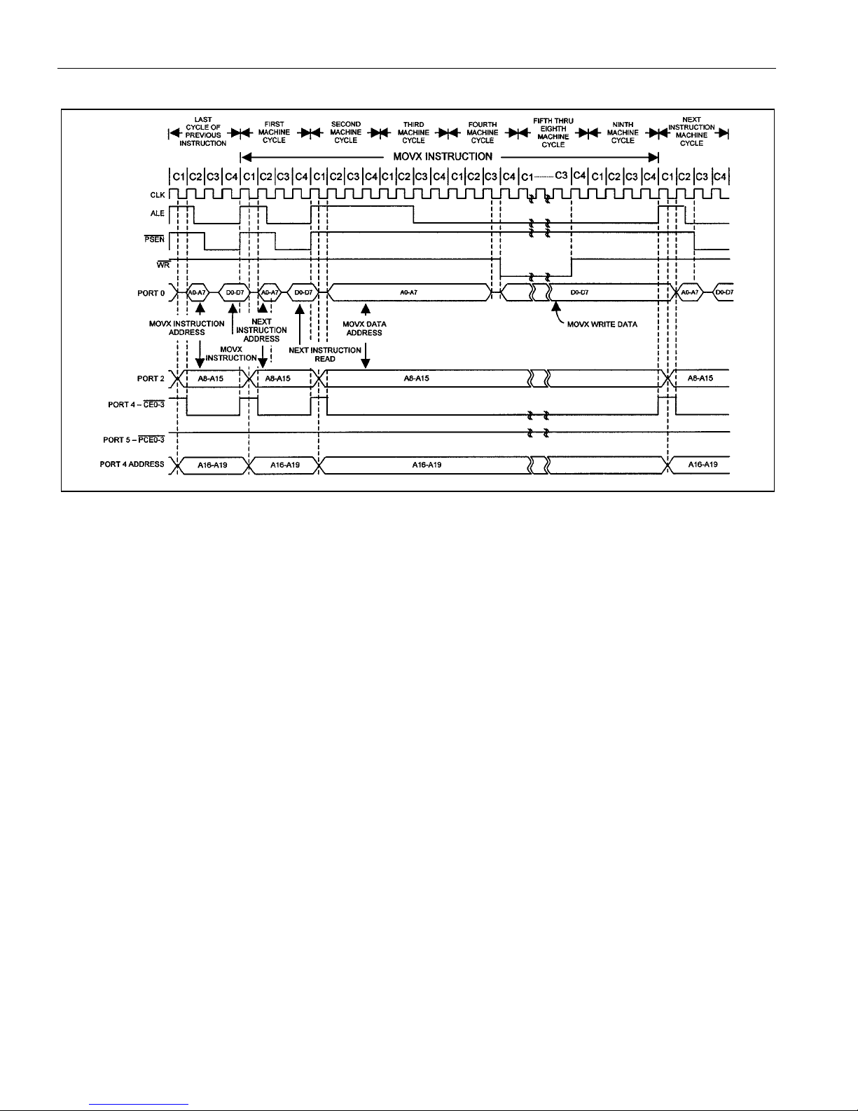
Figure 12. Multiplexed 9-Cycle Data Memory CE0-3 Write
12 of 54
DS80C390 Dual CAN High-Speed Microprocessor
ELECTRICAL CHARACTERISTICS—(NONMULTIPLEXED ADDRESS/DATA BUS)
(Note 13)
PARAMETER SYMBOL CONDITIONS
Oscillator Frequency 1 / t
PSEN Pulse Width
PSEN Low to Valid Instruction In
Input Instruction Hold After PSEN
Input Instruction Float After PSEN
Port 1 Address, Port 4 CE to Valid
Instruction In
Port 2, 4 Address to Valid Instruction
In
Note 13:
All parameters apply to both commercial and industrial temperature operation unless otherwise noted. The value t
the machine cycle clock in terms of the processor’s input clock frequency. These relationships are described in the Stretch Value
Timing table. All signals characterized with load capacitance of 80pF except Port 0, ALE, PSEN, RD, and WR with 100pF. Interfacing
to memory devices with float times (turn off times) over 25ns can cause bus contention. This does not damage the parts, but causes
an increase in operating current. Specifications assume a 50% duty cycle for the oscillator. Port 2 and ALE timing changes in relation
to duty cycle variation. Some AC timing characteristic drawings contain references to the CLK signal. This waveform is provided to
assist in determining the relative occurrence of events and cannot be used to determine the timing of signals relative to the external
clock.
External oscillator 0 40 0 40
CLCL
External crystal 1 40 1 40
0.5 t
t
PLPH
t
0.5 t
PLIV
t
0 0 ns
PXIX
t
PXIZ
t
0.75 t
AVIV1
0.875 t
t
AVIV2
40MHz VARIABLE CLOCK
MIN MAX MIN MAX
- 8 ns
MCS
- 20 ns
MCS
See MOVX
Characteristics
- 22 ns
MCS
- 30 ns
MCS
is a function of
MCS
UNITS
MHz
ns
Figure 13. Nonmultiplexed External Program Memory Read Cycle
13 of 54
DS80C390 Dual CAN High-Speed Microprocessor
MOVX CHARACTERISTICS (NONMULTIPLEXED ADDRESS/DATA BUS)
PARAMETER SYMBOL MIN MAX UNITS
RD Pulse Width
WR Pulse Width
RD Low to Valid Data In
Data Hold After Read t
Data Float After Read t
Port 1 Address, Port 4 CE, Port 5
PCE to Valid Data In
Port 2, 4 Address to Valid Data In t
Port 0 Address, Port 4 CE, Port 5
PCE to RD or WR Low
Port 2, 4 Address to RD or WR Low
Data Valid to WR Transition
Data Hold After WR High
RD or WR High to ALE, Port 4 CE or
Port 5 PCE High
t
RLRH
t
WLWH
t
RLDV
0 ns
RHDX
RHDZ
t
AVDV1
AVDV2
0.5 t
C
0.5 t
C
ST
ST
0.25 t
t
AVWL1
0.5 t
2.5 t
0.375 t
0.625t
t
AVWL2
2.625 t
t
-8 ns
QVWX
0.25 t
t
WHQX
0.5t
1.5 t
t
WHLH
0.25 t
1.25 t
- 6 CST = 0
MCS
x t
- 6
MCS
- 6 CST = 0
MCS
x t
- 6
MCS
0.5 t
C
0.125 t
0.375t
1.375 t
0.75 t
(4CST + 0.5) x t
(4C
ST
0.75 t
(4CST + 0.625) x t
(4CST + 2.625) x t
- 11 CST = 0
MCS
- 11
MCS
- 11
MCS
- 11 CST = 0
MCS
- 11
MCS
- 11
MCS
- 8 CST = 0
MCS
- 10
MCS
- 10
MCS
- 20 CST = 0
MCS
x t
ST
+ 2.5) x t
- 25
MCS
- 5 CST = 0
MCS
- 5
MCS
- 5
MCS
- 26 CST = 0
MCS
- 30
MCS
- 30
MCS
- 30 CST = 0
MCS
- 30
MCS
- 30
MCS
ns
ns
ns
ns
ns
ns
ns
ns
ns
-5 10 CST = 0
- 7 0.25 t
MCS
- 7 1.25 t
MCS
MCS
MCS
+ 10
+ 10
ns
STRETCH
VALUES
(MD2:0)
C
ST
£ 7
1 £ C
ST
1 £ C
£ 7
ST
£ 7
1 £ C
ST
£ 3
1 £ C
ST
4 £ C
£ 7
ST
£ 3
1 £ C
ST
4 £ C
£ 7
ST
£ 3
1 £ C
ST
£ 7
4 £ C
ST
£ 3
1 £ C
ST
£ 7
4 £ C
ST
£ 3
1 £ C
ST
4 £ C
£ 7
ST
£ 3
1 £ C
ST
£ 7
4 £ C
ST
£ 3
1 £ C
ST
4 £ C
£ 7
ST
14 of 54
DS80C390 Dual CAN High-Speed Microprocessor
Figure 14. Nonmultiplexed 9-Cycle Address/Data CE0-3 MOVX Read/Write Operation
15 of 54
DS80C390 Dual CAN High-Speed Microprocessor
Figure 15. Nonmultiplexed 9-Cycle Address/Data PCE0-3 MOVX Read/Write Operation
16 of 54
DS80C390 Dual CAN High-Speed Microprocessor
Figure 16. Nonmultiplexed 2-Cycle Data Memory 3-PCE0 Read or Write
Figure 17. Nonmultiplexed 2-Cycle Data Memory CE0-3 Read
17 of 54
 Loading...