

Dallas DS1666, DS1666S Service Manual
DS1666, DS1666S
DS1666, DS1666S
Audio Digital Resistor
FEATURES
• 128 position, digitally controlled potentiometer
• Operates from a +5 volts power supply with TTL sig-
nal inputs
• Wide analog voltage range of ±5 volts
• Resistive elements are temperature compensated to
±20 percent end to end
• Low–power CMOS
• 14–pin DIP or 16–pin SOIC for surface mount applica-
tions
• Default position on power up sets wiper position at
10%
• Operating temperature range
– –40°C to +85°C; industrial
Resistance values Low End High End –3dB Point
DS1666–10 10KΩ 24Ω 152Ω 1.1 MHz
DS1666–50 50KΩ 122Ω 759Ω 200 KHz
DS1666–100100KΩ 243Ω 1.519KΩ 100 KHz
DESCRIPTION
The DS1666 is a solid–state potentiometer which is set
to value by digitally controlled resistive elements. The
potentiometer is composed of 127 resistive sections.
Between each resistive section and both ends of the potentiometer are T AP points accessible to the wiper. The
position of the wiper on the resistance array is controlled
by the CS
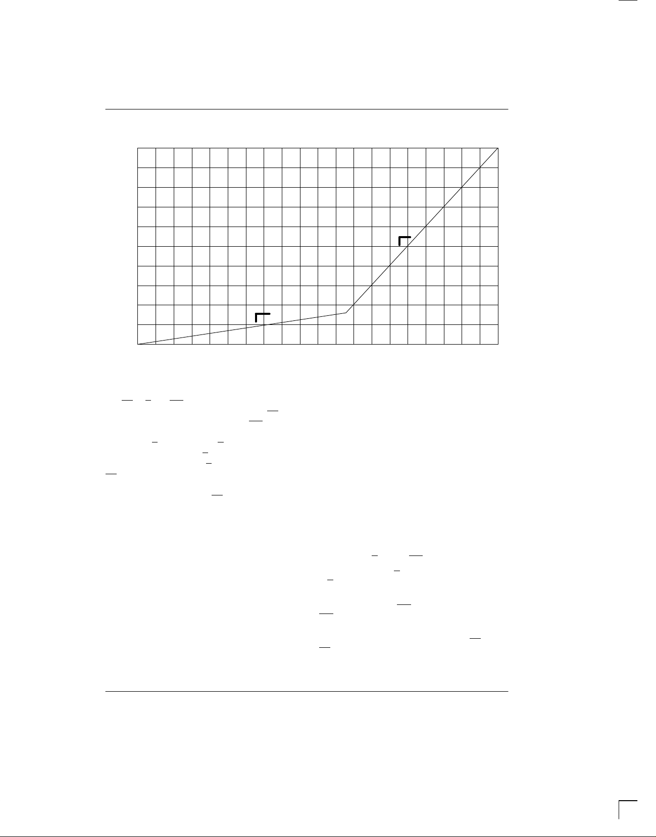
defaults to the 10% position on power up. The resolution of the DS1666 is shown in Figure 1.
, U/D and INC inputs. The position of the wiper
Resolution/Step
PIN ASSIGNMENT
1
NC
2
U/D
3
INC
4
CS
GND
5
NC
6
NC
7
14–PIN DIP (300 MIL)
See Mech. Drawings Section
U/D
NC
NC
INC
NC
CS
NC
GND
1
2
3
4
5
6
7
8
16–PIN SOIC (300 MIL)
See Mech. Drawings Section
NC
14
V
13
CC
12
V
B
11
V
W
V
10
H
V
9
L
8
NC
16
V
CC
15
NC
14
V
B
13
V
W
12
V
H
11
NC
10
NC
9
V
L
PIN DESCRIPTION
V
H
V
L
V
W
U/D
INC – Wiper Movement Control
CS – Chip Select for Wiper Movement
NC – No Connection
V
CC
GND – Ground
V
B
The DS1666 Digital Audio Resistor is uniquely designed
to provide a potentiometer that is logarithmic rather than
linear across its entire range. The lower half of the potentiometer advances 1% of total resistance for each
3% of scale advanced, providing for precise amplification of low volume signals. The upper half of the potentiometer advances 2% of resistance for every 1% of
scale advanced, providing for the lower resolution gain
required for high volume amplification.
– High Terminal of Resistor
– Low Terminal of Resistor
– Wiper Terminal of Resistor
– Up/Down Control
– +5 Volts
– 0 to –5 Volts
022698 1/7
DS1666, DS1666S
GRAPH OF AUDIO TAPER Figure 1
100
90
80
70
60
50
40
30
20
PERCENT TOTAL RESISTANCE
10
0
0 5 10 15 20 25 30 35 40 45 50 55 60 65 70 75 80 85 90 95 100
LOW TERMINAL
3
1
% OF ACTIVE DIGITAL TAPS
OPERATION
The CS, U/D and INC inputs control the position of the
wiper along the resistor array (Figure 1). When CS
tive (low), a high to low transition on the INC will increment or decrement an internal counter depending on the
level of the U/D pin. When the U/D pin is low, the counter
will decrement. When the U/D
increment. The state of the U/D
is active allowing for precise adjustment during cali-
CS
pin is high, the counter will
pin can be changed while
bration. The output of the counter is decoded to set the
position of the wiper. When the CS input transitions to the
high (inactive) level, the value of the counter is stored and
the wiper position is maintained until power (VCC) is lost.
When power is restored, the DS1666 returns to the default setting and positions the wiper to 10 percent. The
value of the end–to–end and end–to–wiper position is indeterminate while V
is not applied.
CC
The DS1666 has a resistor array that resembles an audio taper potentiometer as shown in Figure 1 1. Since
the taper is not linear, exact resistance values for each
of the 128 positions of the resistor is not specified. However, the end-to-end resistance is specified to be within
±20 percent of the stated resistor value over an industrial temperature range of –40°C to +85°C.
is ac-
1
2
HIGH TERMINAL
ANALOG CHARACTERISTICS
End–to–End Resistance Tolerance = ±20 percent
Typical Noise = <120 dB/Hz REF:IV
T emperature Coef ficient = ±800 PPM/°C typical
Resistance at tap #74=18% ± 2% of total resistance.
PIN DESCRIPTIONS
V
H
V
L
V
W
Up/Down The U/D
(U/D
) tion of the wiper movement when setting
Increment Toggling INC
(INC
) ter wiper by either incrementing or decre-
Chip Select The device is selected when CS
(CS
) low. The current counter value is stored
The high end of the potentiometer. This
terminal is capable of handling input voltages between ±5 volts.
The Low end of the potentiometer. This
terminal is capable of handling input voltages between ±5 volts.
The wiper terminal of the potentiometer.
The value of the wiper is controlled by the
U/D
and the INC pins.
input controls the direc-
the potentiometer.
will move the potentiome-
menting the counter.
input is
when CS is returned high.
022698 2/7
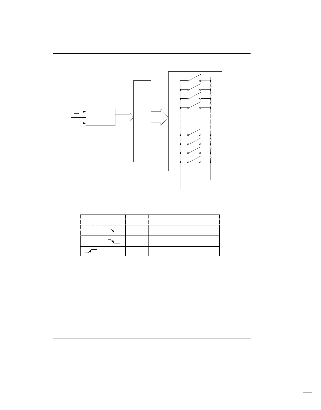
BLOCK DIAGRAM Figure 2
DS1666, DS1666S
U/D
INC
CS
7 BIT
COUNTER
MODE SELECTION Figure 3
WIPER
POSITION
DECODE
1 OF 128
TRANSFER LOGIC ARRAY
V
H
V
L
V
W
CS INC U/D MODE
L H WIPER UP
L L WIPER DOWN
H X STORE WIPER POSITION
022698 3/7
 Loading...