

Daewoo Semiconductor DMC73CE167, DMC73C167 Datasheet

1
8Bit Single Chip Microcontroller DMC73C167
1. Introduction
1.1 Description
2
1.2 Pin Configurations
2
1.3 Features
3
2. Device Functions
2.1 Block Diagram
5
2.2 Pin Description
6
3. Electrical Specifications
3.1 Absolute Maximum Ratings
8
3.2 Recommended operating conditions
9
3.3 Electrical characteristics
10
3.4 AC Charcteristics
11
3.5 I/O Circuits
14
4. Architecture
4.1 Overview
16
4.2 Register File
16
4.3 Peripheral File (PF)
17
4.4 Stack Pointer (SP)
18
4.5 Status Register (ST)
18
4.6 Program Counter (PC)
19
4.7 Peripheral File Map
19
4.8 Interrupt and Reset Priorities
22
5. Function
5.1 Input/Output Ports
24
5.2 Device Initialization 28
5.3 I/O Control Register 28
5.4 Interrupt Logic and External Interrupt 34
5.5 Programmable Timer / Event Counter
37
5.6 A/D Converter
45
5.7 I2C
49
5.8 6-bit PWM (PWM1_0, PWM1_8)
63
5.9 14-bit PWM (PWM0)
68
5.10 On Screen Display
73
6. OTP Deivce Specifications
6.1 Pin Assignment of OTP programming Adapter Board
83
6.2 Package Descriptions (Mechanical Data)
88
* Appendix : OSD Font Design Guide
89
Table of Contents
£Ä£Á£Å£×£Ï£Ï
DAEWOO ELECTRONICS CO., LTD.
2
8Bit Single Chip Microcontroller
DMC73C167
1. INTRODUCTION
1.1 Description
The DMC73C167 is an 8-bit CMOS microcontroller with 16K bytes of on-chip ROM, 256
bytes of on-chip RAM, OSD (On Screen Display), A/D converter, 10 PWM output ports,
three timers, multi-master I2C communications port, 8 output only pins, and 20 normal I/O
pins. The high-performance CPU internal peripherals allow flexible design in industrial
equipment, televisions, camcorders, VCRs, and other home appliances.
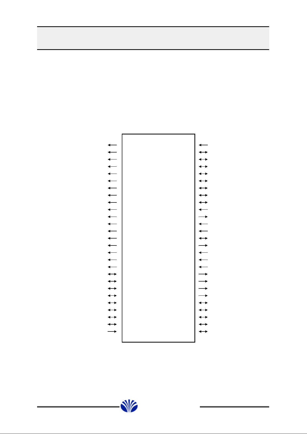
1.2 Pin Configurations
PWM0 (14bit) 1 54 VCC
PWM1_0 (6bit) 2 53 A7
PWM1_1 (6bit) 3 52 SCL
PWM1_2 (6bit) 4 51 SDA
PWM1_3 (6bit) 5 50 A6
PWM1_4 (6bit) 6 49 A5/INT5_0
PWM1_5 (6bit) 7 48 A4/INT3_0
PWM1_6 (6bit) 8 47 A3/INT1
PWM1_7 (6bit) 9 46 A1/ECI1
PWM1_8 (6bit) 10 45 /RESET
B0/T1OUT(OPEN D) 11
DMC73C167
44 OSC OUT(CPU)
B1/T3OUT(OPEN D) 12 43 OSC IN(CPU)
B2(OEPN DRAIN) 13 42 TEST
B3(OEPN DRAIN) 14 41 A2/ECI2
B4(OEPN DRAIN) 15 40 OSC OUT(OSD)
B5(OEPN DRAIN) 16 39 OSC IN(OSD)
B6(OEPN DRAIN) 17 38 /Vsync
B7(OEPN DRAIN) 18 37 /Hsync
A0/4BIT ADC 19 36 Yout or /Yout
C0 20 35 BLUE
C1 21 34 GREEN
C2 22 33 RED
C3 23 32 D3
C4 24 31 D2
C5 25 30 D1
C6 26 29 D0
VSS 27 28 C7
£Ä£Á£Å£×£Ï£Ï
DAEWOO ELECTRONICS CO., LTD.

3
8Bit Single Chip Microcontroller
DMC73C167
1.3 Features
8-bit architecture with CMOS technology
Flexible memory configurations
- 16K-bytes on-chip ROM
- 256-byte on-chip RAM register file
- Memory-mapped I/O ports for easy addressing
Three on-chip timers
- One 16-bit timer with 5-bit prescaler, 16-bit capture latch, and timer outputs
- Two 8-bit timers with 2-bit prescaler, 8-bit capture latch, and timer outputs
- Direct connection of timer clock through I/O ports for event counting
- Generate Internal interrupts and automatic timer reload
One On-chip A/D converter
- 4-bit resolution with successive approximation conversion
- Conversion speed of 40 machine cycles
On-chip OSD generator
- Display pattern : 20 columns x 2 lines (hardware)
20 columns x 12 lines (software)
- Character font : 12 dots x 18 dots
- Number of characters : 128 fonts
- Color : 8 colors per character
Ten PWM D/A converters
- One 14-bit PWM output port with polarity control
- Nine 6-bit PWM output ports with polarity control
On-chip I2C bus interface hardware
- Master mode operation
- Slave mode operation
- Multi-master mode operation
£Ä£Á£Å£×£Ï£Ï
DAEWOO ELECTRONICS CO., LTD.

4
8Bit Single Chip Microcontroller
DMC73C167
Flexible interrupt handling and powerful instruction set
- Three external interrupts with schmitt trigger input
- No limitation on sub-routine calls (dependent on stack size only)
- Software calls through vector table (maximum 24 vectors)
- Software monitoring of interrupt status
- Precise interrupt timing through capture latch
- Global and individual interrupt masking
- Bit, nibble, word manipulation, and multiply / divide instructions
General purpose input/output ports
- Eight output only pins
- 20 input/output pins
Operating range
- CPU clock : 2MHz to 6MHz
- OSD clock : 3MHz to 8MHz
- Temperature :
0 ¡É to 70 ¡É
Package
- Primary : 54-pin Shrink dual in line package
- OTP : 54-pin Shrink dual in line package
Development support
- System evaluation and piggyback prototyping device : SE73CP87B
- Low-cost evaluation module : EVM73C00A and ADP73C167
- OTP : TMS73CE167
- Assembler/linker cross-support for popular hosts
£Ä£Á£Å£×£Ï£Ï
DAEWOO ELECTRONICS CO., LTD.
5
8Bit Single Chip Microcontroller
DMC73C167
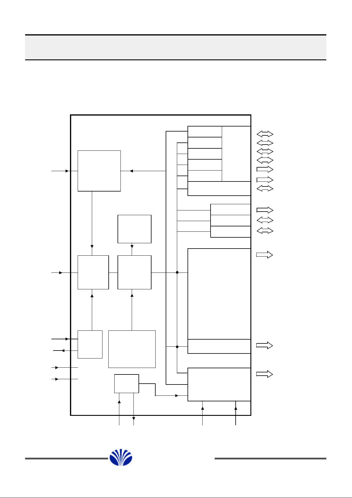
2. DEVICE FUNCTIONS
2.1 Block Diagram
Ext Int
A/D Con
TIMER 1
TIMER 2
TIMER 3
I2C
B PORT
C PORT
D PORT
6-Bit PWM
14-Bit PWM
/RESET
TEST
IN
OUT
VCC
VSS
A PORT
B PORT
Interrupt
Control
On-Screen
Display
RAM
256 Bytes
Peripheral
& Memory
Control
8-Bit
CPU
ROM
16K Bytes
CPU
OSD
OSD
OSC
IN OUT /Hsync /Vsync
A0(ADC)
PWM1_0
PWM1_1
PWM1_2
PWM1_3
PWM1_4
PWM1_5
PWM1_6
PWM1_7
PWM1_8
PWM0
RED
GREEN
BLUE
Yout or /Yout
B0-B7
C0-C7
D0-D3
A1-A2(ECI)
A3-A5(INT)
A6-A7
B0(T1OUT)
B1(T3OUT)
SDA, SCL
£Ä£Á£Å£×£Ï£Ï
DAEWOO ELECTRONICS CO., LTD.
6
8Bit Single Chip Microcontroller
DMC73C167
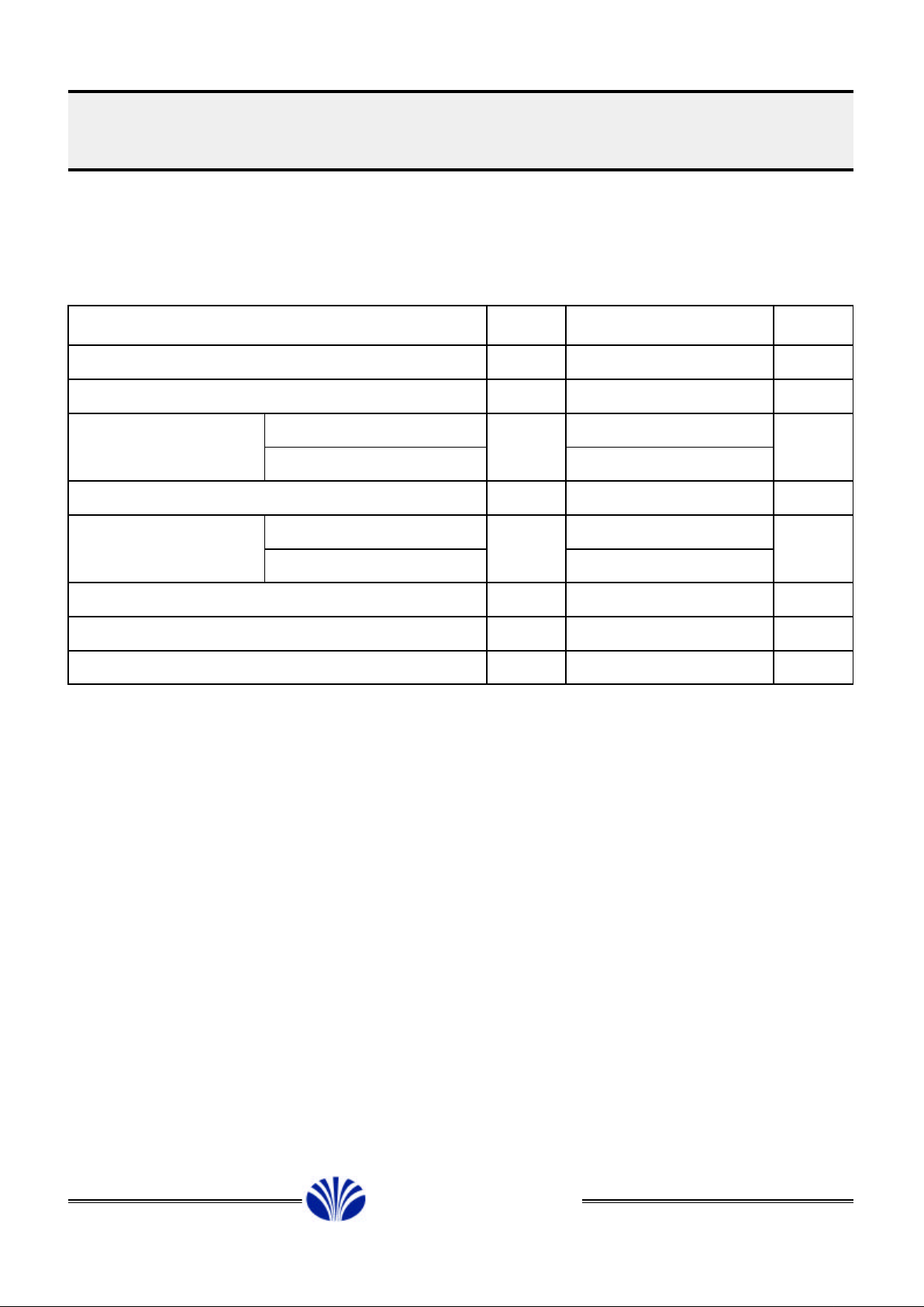
2.2 Pin Description
Pin Pin Number
Symbol Primary SE
PWM0 1 1 O 14-bit PWM output CMOS output
PWM1_0 2 2 O 6-bit PWM output 0 PWM1_0 to PWM1_8
PWM1_1 3 3 O 6-bit PWM output 1 are output pins with
PWM1_2 4 4 O 6-bit PWM output 2 +12V open drain
PWM1_3 5 5 O 6-bit PWM output 3
PWM1_4 6 6 O 6-bit PWM output 4
PWM1_5 7 7 O 6-bit PWM output 5
PWM1_6 8 8 O 6-bit PWM output 6
PWM1_7 9 9 O 6-bit PWM output 7
PWM1_8 10 10 O 6-bit PWM output 8
B0/T1OUT 11 11 O Output, Timer 1 clock out B0 to B3 are optional use
B1/T3OUT 12 12 O Output, Timer 3 clock out for open-drain output
B2 13 13 O Output with +12V buffer
B3 14 14 O Output
B4 15 15 O Output B4 to B7 are optional use
B5 16 16 O Output for open-drain output with
B6 17 17 O Output 12mA drive(+5V) or internal
B7 18 18 O Output pull up(+5V) resistor by mask
option
A0 19 19 I/O ADC input or normal I/O 4-bit A/D converter or normal
I/O internal pull up(+5V)
resistor (mask option)
C0 20 20 I/O Digital I/O C0 to C7 are normal I/O pins
C1 21 21 I/O and internal resistors can be
C2 22 22 I/O optionally pulled up(+5V )
C3 23 23 I/O during masking process
C4 24 24 I/O
C5 25 25 I/O
C6 26 26 I/O
VSS 27 27 I Ground reference
C7 28 38 I/O
D0 29 39 I/O Digital I/O D0 to D3 are normal I/O pins
D1 30 40 I/O and internal resistors can be
D2 31 41 I/O optionally pulled up(+5V)
D3 32 42 I/O during masking process
Function
Description
I/O
£Ä£Á£Å£×£Ï£Ï
DAEWOO ELECTRONICS CO., LTD.
7
8Bit Single Chip Microcontroller
DMC73C167
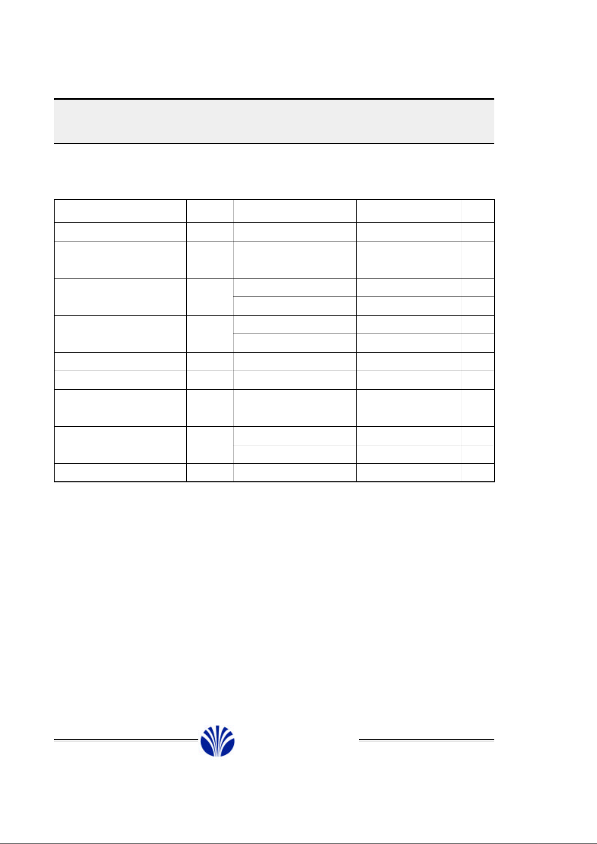
2.2 Pin Description (Continued)
Pin Pin Number
Symbol Primary SE
RED 33 43 O OSD red color output CMOS output
GREEN 34 44 O OSD green color output CMOS output
BLUE 35 45 O OSD blue color output CMOS output
Yout 36 46 O OSD blanking signal Active high or low(mask option)
/HYSNC 37 47 I H SYNC input OSD H position reference
/VSYNC 38 48 I V SYNC input OSD V position reference
OSCI_OSD 39 49 I Clock input for OSD
OSCO_OSD 40 50 O Clock output for OSD
A2(ECI2) 41 51 I/O I/O, Timer 2 clock input Internal pull-up(+5V) resistor
(mask option). Event counter
or normal I/O
TEST 42 52 I Should be fixed to 0 For device test
OSCI_CPU 43 53 I Clock input for CPU
OSCO_CPU 44 54 O Clock output for CPU
/RESET 45 55 I For CPU reset
A1(ECI1) 46 56 I/O I/O, Timer 1 clock input Event counter or normal I/O
A3(INT1) 47 57 I/O External interrupt 1 With Schmitt trigger
A4(INT3_0) 48 58 I/O External interrupt 3_0 With Schmitt trigger
A5(INT5_0) 49 59 I/O External interrupt 5_0 With Schmitt trigger
A6 50 60 I/O Digital I/O A0 to A6 can be optionally pulled
up(+5V) during masking process
SDA 51 61 I/O Data pin for I2C Open drain(+5V) with
SCL 52 62 I/O Clock pin for I2C Schmitt input
A7 53 63 I/O Digital I/O Internal pull-up(+5V) resistor
(mask option)
VCC 54 64 I 4.5V-5.5V
Function
Description
I/O
£Ä£Á£Å£×£Ï£Ï
DAEWOO ELECTRONICS CO., LTD.
8
8Bit Single Chip Microcontroller
DMC73C167
3. ELECTRICAL SPECIFICATIONS
3.1 Absolute Maximum Ratings
Parameter Symbol Rating Unit
Supply voltage range* VCC -0.3 through 7.0 V
Input voltage range VI -0.3 through VCC +0.3 V
Output Port B0-B3, PWM1_n -0.3 through 15.0 V
voltage range Except B0-B3, PWM1_n -0.3 through VCC +0.3
Input current II ±10 mA
Output Port B4-B7 IO Max 20 mA
current Except B4-B7 Max 10
Total low-level output current IOL Max 120 mA
Power dissipation PD 0.5 W
Storage temperature range TSTG -55 through +125
¡É
*Unless otherwise noted, all voltages are with respect to VSS.
Test pin must connect to VSS.
Pull-up resistor option is not counted in the electrical specifications.
Stresses beyond those listed under "Absolute Maximum Ratings" may cause permanent
damage to the device. This is a stress rating only and functional operation of the device
at these or any other conditions beyond those indicated in Section " Recommended
Operating Conditions" of this specification is not implied.
Exposure to absolute-maximum-rated conditions for extended periods may affect
device reliability.
£Ä£Á£Å£×£Ï£Ï
DAEWOO ELECTRONICS CO., LTD.
9
8Bit Single Chip Microcontroller
DMC73C167
3.2 Recommended Operating Conditions
Parameter Symbol Port Min Typ Max Unit
Supply voltage* VCC 4.5 5.5 V
Operating free-air TOPR
-10¡É 70¡É
Deg
temperature range**
High-level input voltage VIH OSC IN*** VCC-0.7 VCC V
Except OSC IN**** VCC-1.0 VCC V
Low-level input voltage VIL OSC IN*** VSS 0.4 V
Except OSC IN**** VSS 1.1 V
Positive-going threshold VT+ # A3-A5, /RESET 2.5 4.0 V
Negative-going threshold VT- # A3-A5, /RESET 1.0 2.0 V
Hysteresis VH # A3-A5, /RESET, /Hsync, 1.0 V
/Vsync, SCL, SDA
Oepn-drain port supply PORT B0-B3, PWM1_n 4.5 12 14.0 V
voltage PORT B4-B7, SCL, SDA 4.5 5 5.5 V
Analog input voltage A0 VSS VCC V
* Ripple must not exceed 50mVp-p
** See A/D Converter Characteristics
*** OSCIN means both CPU and OSD OSCIN
**** Except Schmitt-trigger inputs
££ VCC = 5.0V
£Ä£Á£Å£×£Ï£Ï
DAEWOO ELECTRONICS CO., LTD.
10
8Bit Single Chip Microcontroller
DMC73C167
3.3 Electrical Characteristics
Parameter Symbol Port Min Typ Max Unit
Input current II VI=VSS-VCC ±10.0 mA
High-level output current IOH VOH=VCC-0.5V -0.3 mA
Low-level output current IOL SCL, SDA VOL=0.4V 3 mA
B4-B7 VOL=1.0V 12 16
Except SCL, SDA, B4-B7 1.7
VOL=0.4V
High-level output voltage VOH IOH= -0.3mA VCC-0.5 VCC V
Low-level output voltage VOL IOL=1.7mA 0.4 V
Low-level output B0-B3, PWM1_n VO=12V ±10
leakage current ILEAK Excpet B0-B3, PWM1_n ±10 uA
VO=VCC
Internal pull-up resister II VDD=5.0V VI=VSS -60 -90 -120 uA
option
Clock frequency FOSC CPU clock 3.0 6.0 MHz
OSDCLK OSD clock 4.0 8.0
Input capacitance CI 15.0 pF
Supply current* ICC Operation mode 12.0 20.0 mA
Halt mode 5 20 uA
*All I/O terminals which except CLKIN are open and VCC=5V.
£Ä£Á£Å£×£Ï£Ï
DAEWOO ELECTRONICS CO., LTD.
11
8Bit Single Chip Microcontroller
DMC73C167
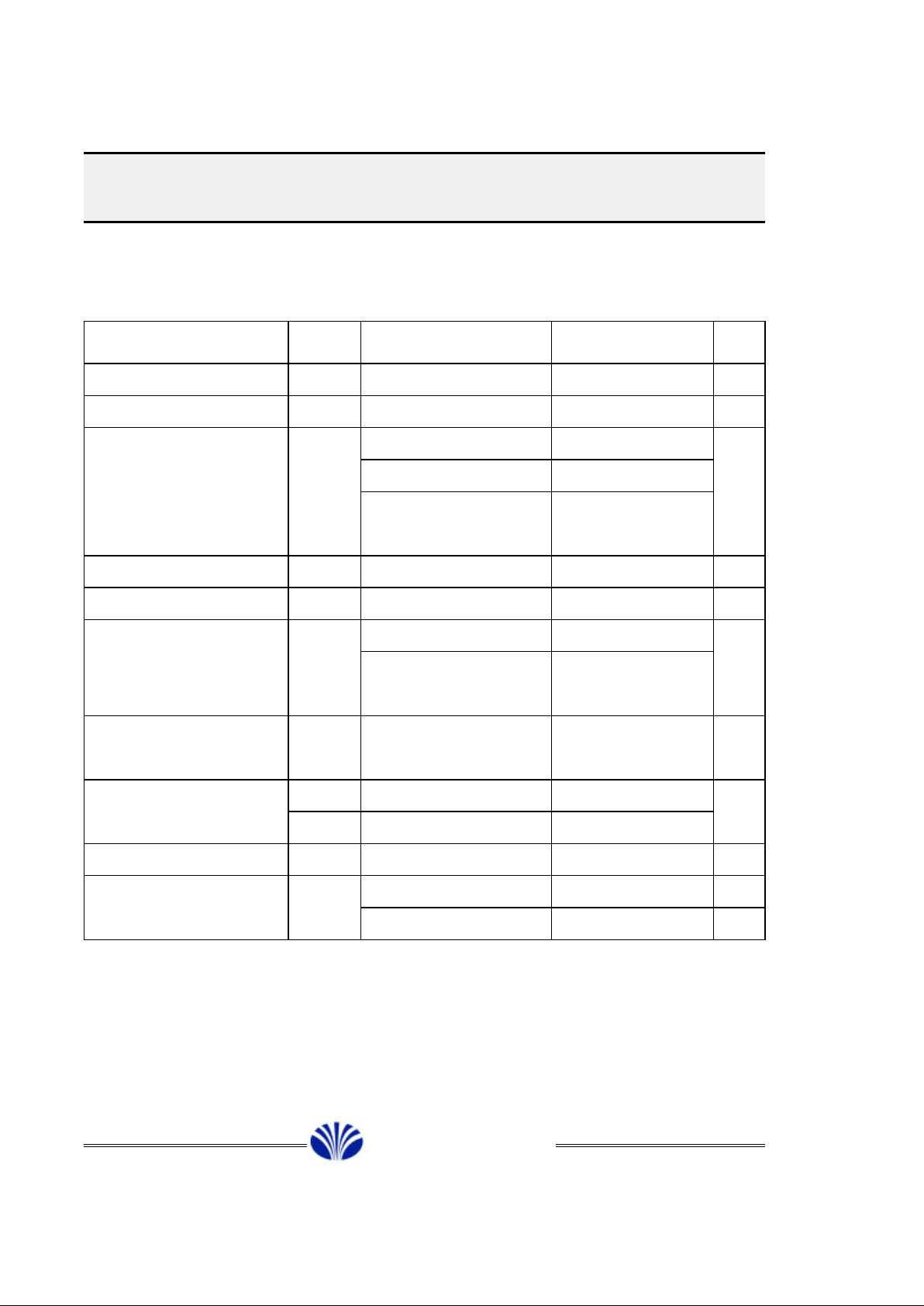
3.4 AC Characteristics
I/O Port
Parameter Port Conditions Min Typ Max Unit
SCL SDA B0-B7 CL=50pF 1 us
I/O Port output PWM1_n*
rise time Except SCL, SDA, CL=15pF 30 60 ns
B0-B7, PWM1_n CL=50pF 150
SCL SDA B0-B7 CL=50pF 1 us
I/O Port output PWM1_n*
fall time Except SCL, SDA, CL=15pF 10 40 ns
B0-B7, PWM1_n CL=50pF 70
* External pull-up registers are needed in PWM1_n, B0-B3.
External pull-up registers are also needed in SCL, SDA. The values would be recommendable
to fit rise and falling time of I2C spec.
Clock I/O
Parameter Symbol Min Typ Max Unit
Rise time tr(c) 20 ns
Clock pulse Fall time tf(c) 10 ns
Duty cycle dty(c) 45 50 55 %
Note : Timing points are 90%(high) and 10%(low).
- Externally Driven Clock Input Waveform -
£Ä£Á£Å£×£Ï£Ï
DAEWOO ELECTRONICS CO., LTD.
XY
DUTY(%) = Tc(c) = X + Y
Tc(c)
X or Y
x 100
12
8Bit Single Chip Microcontroller DMC73C167
3.4 AC Characteristics (Continued)
A/D Converter
Parameter Test Conditions Min Typ Max Unit
Resolution 4 bit
Non-linearity TOPR = -10°through +70°
Zero error VCC = 5V±10% ±1/2 ±1 LSB
Full-scale error VSS = 0V, FOSC = 6MHz
Conversion time* 13.3 uS
* External sample hold circuit is required during 40 machine cycle times. Resolution is dependent
on ripple supply voltage(VCC<VREF). Ripple must not exceed 5mVp-p.
I2C
Parameter Symbol Min Max Unit
SCL clock frequency fSCL 0 100 kHz
Time the bus must be free before
a new transmission can start*
Hold time start condition* tHD;STA 4 us
Low period of the clock* tLOW 4.7 us
High period of the clock* tHIGH 4 us
Setup time for start condition* tSU;STA 4.7** us
Hold time data tHD;DAT 0 us
Setup time data tSU;DAT 250 ns
Rise time of both SDA and SCL lines tR 1 us
Fall time of both SDA and SCL lines tF 300 ns
Setup time for stop condition* tSU;STO 4.7 us
* The value is like above when the digital filter is off. Add 4/Fosc to this value when the
digital filter is on.
** This time must be satisfied by the software delay.
tBUF
4.7
us
£Ä£Á£Å£×£Ï£Ï
DAEWOO ELECTRONICS CO., LTD.
13
8Bit Single Chip Microcontroller DMC73C167
3.4 AC Characteristics (Continued)
I2C (Continued)
SDA
SCL
SDA
SCL
- Timing for I2C Bus -
tBUF
tR tF
tHD;STA
tHD;DAT
tHIGH
tSU;DAT
tHD;STA
tSU;STA
tSU;STO
£Ä£Á£Å£×£Ï£Ï
DAEWOO ELECTRONICS CO., LTD.
tLOW
14
8Bit Single Chip Microcontroller
DMC73C167
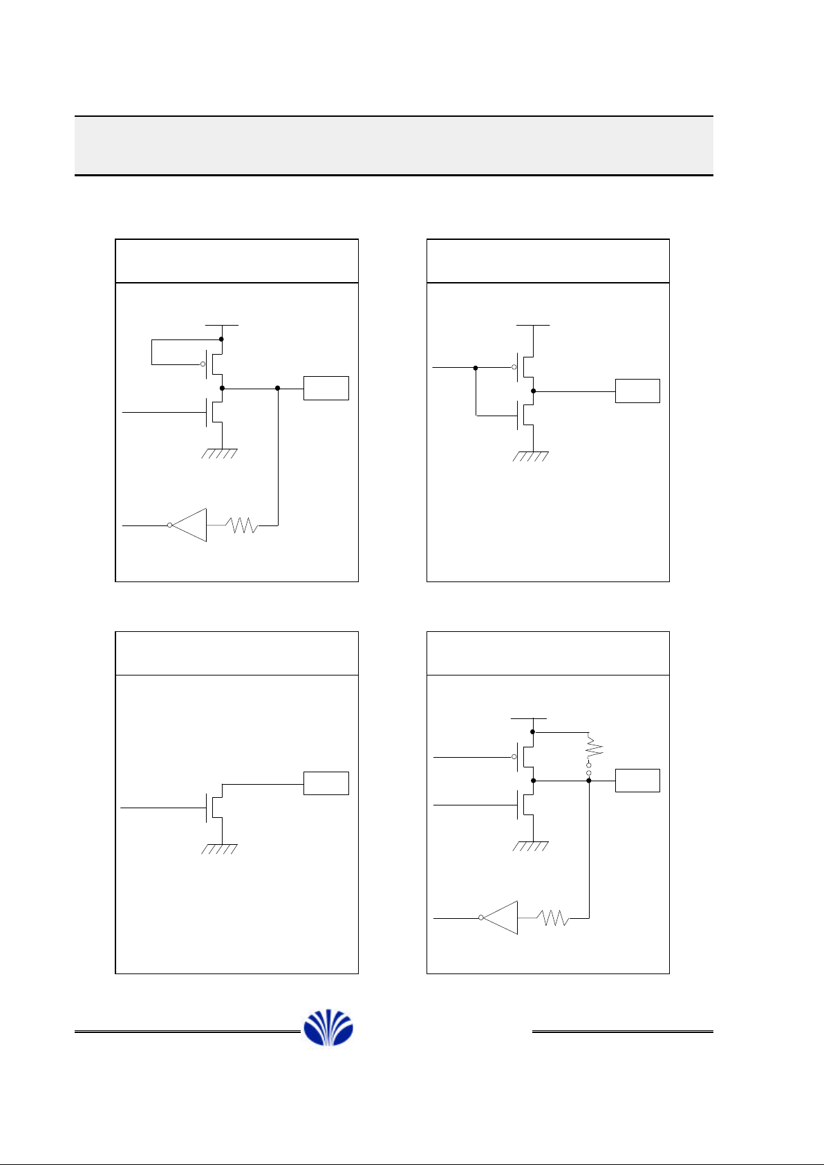
3.5 I / O Circuits
SCL, SDA PWM0, R, G, B, Y
N-CH OPEN DRAIN : 5V CMOS Output
Schmitt Inverter
Port B0-B3, PWM1_0 -PWM1_8 Port A0-A2, A6-A7, C0-C7, D0-D3
N-CH OPEN DRAIN : 12V TEST(SE DEVICE)
(No Inverter on A0 Port)
Vcc
Data Out
Port
Data In
S
Data Out
Port
Data In
Vcc
Data Out
Mask
Option
Vcc
Port
Data Out
Port
Data
Out
£Ä£Á£Å£×£Ï£Ï
DAEWOO ELECTRONICS CO., LTD.
15
8Bit Single Chip Microcontroller
DMC73C167
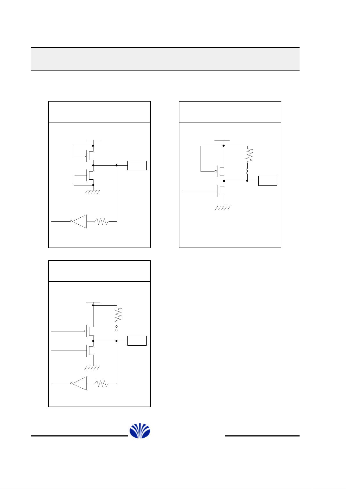
3.5 I / O Circuits (Continued)
/RESET, /Vsync, /Hsync Port B4-B7
TEST(Primary) Input Only OPEN DRAIN : 5V, 12mA
Mask Option
NO : 12mA Current Drive Port
Schmitt Inverter (Except TEST) YES : Internal Pull up
A3, A4, A5
I/O Port
Schmitt Inverter
Vcc
Port
Data In
S
Port
Vcc
Mask
Option
Vcc
Data Out
Port
Data In
S
Mask
Option
Data Out
£Ä£Á£Å£×£Ï£Ï
DAEWOO ELECTRONICS CO., LTD.
16
8Bit Single Chip Microcontroller DMC73C167
4. ARCHITECTURE
4.1 Overview
The DMC73C167 has a maximum memory address space of 16 kbytes on-chip ROM and
only a single-chip mode. On-chip memory spaces are configured as shown if Figure 4-1
below. In the section that follow, the register file(RF) and the peripheral file(PF) are described
along with three important registers in the CPU : the stack pointer(SP), the status register
(ST), and the program counter(PC).
Figure 4-1. DMC73C167 Memory Maps
Memory address
0000h
Register File (RF)
00FFh
0100h
Peripheral File (PF)
01FFh
0200h
Not Available
C005h
C006h
16Kbytes ROM
FFFFh
4.2 Register File (RF)
The 256-byte on-chip RAM resides in locations 0000h to 00FFh of the DMC73C167's
address space and is called the register file (RF). The RAM is treated as a register by much
of the instruction set and is numbered R0-R255. The first two registers, R0 and R1, are also
called the A and B registers, respectively. Several instructions specify A or B as either the
source or destination register. For example, STSP stores the contents of the stack pointer
(SP) in the B register. Except where stated otherwise, any register in the register file can be
addressed as an 8-bit source or destination register. The stack is also located in the register
file. Refer to Section 4.4 for information regarding the initialization of the stack pointer and
stack definition in the register file.
£Ä£Á£Å£×£Ï£Ï
DAEWOO ELECTRONICS CO., LTD.
17
8Bit Single Chip Microcontroller DMC73C167
4.3 Peripheral File (PF)
The peripheral file (PF) resides in location 0100h to 01FFh of the DMC73C167's
address space. Some of the instructions are optimized for efficient access to and from
the registers that reside in the peripheral file. Peripheral file locations are number P0-P255.
The PF registers are used for interrupt control, parallel I/O, timer control, 14-bit
PWM, OSD, 6-bit PWM, I2C and A/D converter control. On screen Display RAM (video
RAM) is also mapped in the peripheral file.
Figure 4-2. DMC73C167 Peripheral File Map
Memory address
100h
P0
: Peripheral Registers
P75
14Bh
14Ch
P76
: Reserved
P95
15Fh
160h
P96
: Line A Video RAM
P115
173h
174h
P116
: Reserved
P127
17Fh
180h
P128
: Line B Video RAM
P147
193h
194h
P148 Not Available
:
P255
1FFh
£Ä£Á£Å£×£Ï£Ï
DAEWOO ELECTRONICS CO., LTD.
18
8Bit Single Chip Microcontroller DMC73C167
4.4 Stack Pointer (SP)
The stack pointer(SP) is an 8-bit register in the CPU which is typically used to hold a pointer
in RAM (the register file). However, the SP can also be used as temporary data storage if a
stack is not implemented, or if the SP contents are not needed.
When a stack is implemented, the SP points to the last or top entry on the stack. The SP
is automatically incremented just before data is pushed onto the stack and automatically
decremented immediately after data is popped from the stack. Upon assertion of the
RESET function (see Section 4.8) 01h is loaded into the SP. The size of the stack can be
changed from the 255-level stack at RESET to a smaller stack by execuiting a stack
initialization program as illustrated in Figure 4-3. This feature allows the stack to be located
anywhere in the register file. The SP is initialized through the B register (R1).
Figure 4-3. Example of Stack Initialization in the Register File
4.5 Status Register (ST)
The status register(ST) is an 8-bit register in the CPU that contains three conditional status
bits : carry(C), sign(N), and zero(Z). It also contains a global interrupt enable bit(I) as shown
in Figure 4-4 below.
Figure 4-4. Status Register (ST)
Bit 7 6 5 4 3 2 1 0
Con C N Z I Future use
C = carry out, N=sign, Z = zero, I = Interrupt enable
0001h
0002h
0003h
0004h
0005h
0006h
01h
ST
PCH
PCL
04h
PCH
PCL 06h
RFSPRF
RFSPCall
£Ä£Á£Å£×£Ï£Ï
DAEWOO ELECTRONICS CO., LTD.
19
8Bit Single Chip Microcontroller DMC73C167
The C, N and Z bits are used mostly for arithmetic operations, bit rotating, and conditional
branching. The carry (C) bit is used as the carry-in and the carry-out for most of the rotate
and arithmetic instructions. The sign(N) bit contains the most significant bit of the
desitination operand contents after instruction execution. The zero(Z) bit contains a 1 when
all bits of the destination operand are equal to zero after instruction execution.
The C, N, and Z status bits also have jump-on-condition instructions associated with them.
The global interrupt enable(I) bit must be set to 1 by the EINT instruction in order for any of
the individual interrupts (INTn) to be recognized by the CPU. The interrupt enable(I) bit can
be cleared by the DINT instruction or by execuiting a device RESET (see Section 4.8).
4.6 Program Counter (PC)
The DMC73C167's 16-bit program counter (PC) consists of two 8-bit registers in the
CPU which contain the MSB and the LSB, respectively, of a 16-bit address , the program
counter high (PCH) and program counter low (PCL). The PC acts as the 16-bit address
pointer of the opcodes and operands in the memory of the currently executing instruction.
Upon assertion of the RESET function, the MSB and the LSB of the PC are loaded into the
A and B registers of the register file (see Section 4.8).
4.7 Peripheral File Map
The peripheral file(PF) resides in location 0100h through 01FFh of the DMC73C167's
address space, as shown in Tables 4-2.
Note : The right-end column, headed "Value After Reset", indicates a reset initial value as
shown in Table 4-1.
Table 4-1. Description of "Value After Reset"
MSB LSB
7 6 5 4 3 2 1 0
- - X X O O 1 1
Becomes value "1" after RESET
Becomes value "0" after RESET
Unkown value after RESET
Not Used
£Ä£Á£Å£×£Ï£Ï
DAEWOO ELECTRONICS CO., LTD.

20
8Bit Single Chip Microcontroller DMC73C167
Table 4-2. Peripheral File Map
Value after Reset
MSB LSB
Number Address Label R/W Contents 5
P0 0100h IOCTL0 R/W Interrupt control 0
P1 0101h IOCTL1 R/W Interrupt control 1 - - - P2 0102h IOCTL2 R/W Interrupt control 2 - - - - P3 0103h IOCTL3 R/W Interrupt control 3 0
P4 0104h IOCTL4 R/W Interrupt control 4 - - 0
P5 0105h - - Reserved
P6 0106h ADATA R A Port data X X X XXXXX
P7 0107h ADIR R/W A Port direction register 0
P8 0108h BDATA R/W B Port data 1
P9 0109h - - Reserved
P10 010Ah CDATA R/W C Port data XX X XX X XX
P11 010Bh CDIR R/W C Port direction 0
P12 010Ch DDATA R/W D Port data - - - - XXX X
P13 010Dh DDIR R/W D Port direction - - - P14 010Eh - - Reserved
P15 010Fh - - Reserved
P16 0110h ADCTL R/W A/D control - 0
P17 0111h ADDATA R A/D data - - - P18 0112h - - Reserved
P19 0113h - - Reserved
P20 0114h T1MSD R/W Timer 1 MS data XX X X XX X X
P21 0115h T1LSD R/W Timer 1 LS data X X X X XX X X
P22 0116h T1CTL0 R/W Timer 1 control X XX X XX
P23 0116h T1CTL1 R Timer 1 control 1 X X XX X XX
P24 0117h T2DATA R/W Timer 2 data XX X X XX X X
P25 0119h T2CTL R/W Timer 2 control X X X XX X
P26 011Ah T3DATA R/W Timer 3 data XX X X XX X X
P27 011Bh T3CTL R/W Timer 3 control - - - - XX
P28 011Ch - - Reserved
P29 011Dh - - Reserved
P30 011Eh - - Reserved
P31 011Fh - - Reserved
P32 0120h PWM0CTL R/W 14-bit PWM control - - - - P33 0121h WAKEMS R/W Wake up MS counter - - 0
P34 0122h WAKELS R/W Wake up LS counter 0
P35 0123h PWM0AT W 14-bit PWM add time - - 0
P36 0124h PWM0BT W 14-bit PWM base time 0
P37 0125h PWM1CTL R/W 6-bit PWM control - - - - - - P38 0126h PWM1_0T W PWM1_0 polarity and time - 0
P39 0127h PWM1_1T W PWM1_1 polarity and time - 0
P40 0128h PWM1_2T W PWM1_2 polarity and time - 0
£Ä£Á£Å£×£Ï£Ï
DAEWOO ELECTRONICS CO., LTD.

21
8Bit Single Chip Microcontroller DMC73C167
Table 4-2. Peripheral File Map (Continued)
Value after Reset
MSB LSB
Number Address Label R/W Contents 5
P41 0129h PWM1_3T W PWM1_3 polarity and time - 0
P42 012Ah PWM1_4T W PWM1_4 polarity and time - 0
P43 012Bh PWM1_5T W PWM1_5 polarity and time - 0
P44 012Ch PWM1_6T W PWM1_6 polarity and time - 0
P45 012Dh PWM1_7T W PWM1_7 polarity and time - 0
P46 012Eh PWM1_8T W PWM1_8 polarity and time - 0
P47 012Fh - - Reserved
P48 0130h MCTL0 R/W I2C master control 0 - 0
P49 0131h MCTL1 R/W I2C master control 1 - - - P50 0132h MSTS R/W I2C master status 0 - - - P51 0133h MDATA R/W I2C master data X X X XX X XX
P52 0134h HDC R/W I2C master high duration X X X X XX X X
P53 0135h LDC R/W I2C master low duration XX X XX X XX
P54 0136h SADDR W I2C slave address XX X X X XX X
P55 0137h SDATA R/W I2C slave data X X X XX X XX
P56 0138h SCTL R/W I2C slave control - - P57 0139h DFCTL R/W I2C digital filter control - - - - - P58-P67 013Ah-0143h - - Reserved for on-chip PF
P68 0144h OSDCTL R/W OSD control register - - P69 0145h OSDHP W OSD horizontal position - 1
P70 0146h OSDVPA W LINE A vertical position 1
P71 0147h OSDVPB W LINE B vertical position 1
P72 0148h VPCNTR R Vertical display counter - - - P73-P75 0149h-014Bh - - Reserved
P77-P95 0150h-015Fh - - Reserved for on-chip PF
P96-P115 0160h-0173h - W OSD LINE A video RAM XX X X XX X X
P128-P147
0180h-0193h - W OSD LINE B video RAM XX X X X XX X
P148-P255
0194h-01FFh - - Not available
£Ä£Á£Å£×£Ï£Ï
DAEWOO ELECTRONICS CO., LTD.

22
8Bit Single Chip Microcontroller DMC73C167
4.8 Interrupt and Reset Priorities
The DMC73C167 has priority servicing of five interrupt levels and RESET. These levels
are defined as shown in Table 4-3. The TRAP instructions branch to two-byte location in a
reserved section of memory called the TRAP vector table. As shown in Figure 4-5. each trap
location stores a 16-bit address that references either the reset function (TRAP0), one of the
five interrupt service routines (TRAP1-INT1, TRAP2-INT2, TRAP3-INT3, TRAP4-INT4, TRAP5INT5), or a subroutine (TRAP6-23). Once the interrupt has been acknowledged, the CPU then
pushes the contents of the status register and the program counter (MSB and LSB) onto the
stack and zeros the status register, including the global interrupt Enable (I) bit.
The CPU reads an interrupt code from the interrupt logic and branches to the address
contained in the corresponding interrupt vector location in memory. The interrupt service routine
can explicitly enable nested interrupts by executing the EINT instruction to directly set the I bit
in the status register to 1, thus permitting routine is completed, it returns to the previous interrupt
service routine by executing the RETI instruction.
Table 4-3. Interrupt and Reset Priorities
Level Name Source Trigger Factor Vector
MSB LSB
0 /Reset External Active Low FFFEh FFFFh
1 INT1 External Falling/Rising FFFCh FFFDh
2 INT2_0 Timer 1 Timer 1 underflow FFFAh FFFBh
INT2_1 Timer 2 Timer 2 underflow
3 INT3_0 External Falling/Rising FFF8h FFF9h
INT3_1 Timer 3 Timer3 underflow
4 INT4 OSD OSD enable FFF6h FFF7h
5 INT5_0 External Falling/Rising FFF4h FFF5h
INT5_1 12C master Data ready from slave
INT5_2 12C slave Slace address selected
£Ä£Á£Å£×£Ï£Ï
DAEWOO ELECTRONICS CO., LTD.
23
8Bit Single Chip Microcontroller DMC73C167
Figure 4-5. TRAP Vector Table
Address
FFD0h TRAP23 (MSB) *
FFD1h TRAP23 (LSB) **
/ ////////
FFEFh TRAP8 (A0-A7)
FFF0h TRAP7 (MSB)
FFF1h TRAP7 (LSB)
FFF2h TRAP6 (MSB)
FFF5h INT5 or TRAP5 (LSB)
FFF7h INT4 or TRAP4 (LSB)
FFF8h INT3 or TRAP3 (MSB)
FFF9h INT3 or TRAP3 (LSB)
FFFAh INT2 or TRAP2 (MSB)
FFFBh INT2 or TRAP2 (LSB)
FFFCh INT1 or TRAP1 (MSB)
FFFDh INT1 or TRAP1 (LSB)
FFFEh RESET or TRAP0 (MSB)
FFFFh RESET or TRAP0 (LSB)
* MSB = A8-A15
** LSB = A0-A7
£Ä£Á£Å£×£Ï£Ï
DAEWOO ELECTRONICS CO., LTD.

24
8Bit Single Chip Microcontroller DMC73C167
5. FUNCTION
5.1 Input/Output Ports
The DMC73C167 has 28 I/O pins organized as four parallel ports labeled
A, B, C and D. Each port is mapped into 4- to 8-bit data value resiters in the peripheral file (PF).
The data value registers are usually called APORT, BPORT, CPORT and DPORT in a program.
Ports A, C and D are implemented as bidirectional I/O ports.
Port B is an open-drain output only port with a 12 V buffer (B0-B3)and 12mA current drive
capability (B4-B7).
Each bidirectional port (that is, Port A, C and D) has a corresponding data direction register
(DDR) that programs each I/O pin as an input or output pin. A bit set to 1 in the DDR will
cause the corresponding pin to be an output pin, while a 0 in the DDR will turn the pin into
a high-impedance input pin. Upon RESET, the DDR filp-flop registers are set to 0 by the
on-chip circuitry, forcing them to become inputs. Also upon RESET, the output data registers
of the output only port (that is, Port B) are set to 1 by the on-chip circuitry. And, other output
data registers are indeterminated data set.
After RESET, if 1s are writtern to the DDR register sometime before the output data register
is changed, then the corresponding I/O pins will output a 1. For this reason, it is good
practice to load the output data registers of Ports A, C and D with the desired value before
any bits are configured as outputs. In addition, DMC73C167 has several mask options
related to the I/O pins such as pull-up resistors. Those I/O pins are individually configurable
at the masking stage. For a detailed description of the I/O pins in the DMC73C167,
see table 3-2.
5.1.1 A Port
Pins A0 to A7 of A port are bidirectional I/O ports and several hardware-related functions are
interfaced with the CPU through this port. Pin A0 can be used as an analog input for the onchip A/D converter. Pin A1 and A2 can be used for the event counter input of Timer 1 and
Timer 2, respectively. Pin A3, A4 and A5 can be used for the Schmitt-buffered external interrupt
input for INT1, INT3_0, and INT5_0, respectively.
Reading the port - A data register (P6) returns each value at the A0 - A7 pins if the
corresponding DDR bit is set to 0 and returns each output buffer register value if the DDR
bit is 1. The user can specify internal pull-up (5V) resistor insertion or not selectively for port
A pins (mask option).
Table 5-1. P7 0107h ADDR A Port Direction
Bit 7 6 5 4 3 2 1 0
R
W
ADDR7 ADDR6 ADDR5 ADDR4 ADDR3 ADDR2 ADDR1 ADDR0
£Ä£Á£Å£×£Ï£Ï
DAEWOO ELECTRONICS CO., LTD.
25
8Bit Single Chip Microcontroller DMC73C167
Table 5-2. P6 0106h ADATA A Port Data
Bit 7 6 5 4 3 2 1 0
R
W
ADATA7 ADATA6 ADATA5 ADATA4 ADATA3 ADATA2 ADATA1 ADATA0
Special - - INT5_0 INT3_0 INT1 ECI2 ECI1 ADIN
Table 5-3. A Port Control Register Operation
ADDRn Driection ADATAn(Read) ADATAn(Write)
0 Input Port 0 ; Input 'Low' Invalid
1 : Input 'High'
1 Output Port Written Data 0 ; Output 'Low'
1 : Output 'High'
Note :
Special usage for Pin A0 to A5 is as follows.
ADIN : Analog signal for 4-bit ADC is acceptable through Pin A0. Bit 0 for the A/D
control register (ADCTL, P16) controls digital input or analog input.
To use analog input, pin A0 must be in input mode (ADDR0-0).
ECI1 : Event counter input for Timer 1
The external clock from Pin A1 can be directly connected to the clock source of
Timer 1. T1SRC (bit 5 of P22) selects the source of Timer 1.
See Timer 1 operation for more details.
ECI2 : Event counter input for Timer 2.
The external clock from Pin A2 can be directly connected to the clock source of
Timer 2. T2SRC (bit 5 of P25) selects the source of Timer 2.
See Timer 2 operation for more details.
INT1 : External interrupt 1 is triggered by the falling and rising transition of Pin A3,
which must be in input mode to be used as an interrupt source. This pin
can also be used as a normal input port while the interrupt is activated.
INT3_0 : External interrupt 3_0 is triggered by the falling and rising transition of
Pin A4, which must be in input mode to be used as an interrupt source.
This pin can also be used as a normal input port while the interrupt is
activated.
£Ä£Á£Å£×£Ï£Ï
DAEWOO ELECTRONICS CO., LTD.
26
8Bit Single Chip Microcontroller DMC73C167
INT5_0 : External interrupt 5_0 is triggered by the falling and rising transition of
Pin A5, which must be the input mode to be used as an interrupt source.
This pin can also be used as a normal input port while the interrupt is
activated.
5.1.2 B Port
Pins B0 to B7 of B Port are output only pins. Pins B0 to B3 contain a high-voltage buffer (12V
nominal) with open-drain output and Pins B4 to B7 contain a high-current output buffer (12mA
nominal). Pins B0 and B1 can be used as the clock output of Timer 1 and Timer 3,
respectively. in the DMC73C167, the user can specify the internal pull-up (5V) resistor
for the B4 to B7 ports selectively (mask option).
Table 5-4. P8 0108h BDATA B Port Data
Bit 7 6 5 4 3 2 1 0
R
W
BDATA7 BDATA6 BDATA5 BDATA4 BDATA3 BDATA2 BDATA1 BDATA0
Special - - - - - - T3OUT T1OUT
The B Port control register operation is as follows.
WRITE : Setting the BDATAn bit to 1 outputs logic high status to the same pin
number and setting BDATAn bit to 0 outputs logic low status to the
same pin number.
READ : External pins are not accessed through the read operation. The CPU
can read data from B Port but it is the contents of the output buffer
register written by the CPU previously.
Note : Special usage for Pins B0 and B1 is as follows.
T1OUT : Clock output for Timer 1
Underflow of Timer 1 MSB decrement register toggles the logic level of Pin B0
When bit 6 of T1CTL0 (P22) is set to 1.
T3OUT : Clock output for Timer 3
Underflow of Timer 3 decrement register toggles the logic level of Pin B1 when
bit 6 of T2CTL (P25) is set to 1.
£Ä£Á£Å£×£Ï£Ï
DAEWOO ELECTRONICS CO., LTD.
27
8Bit Single Chip Microcontroller DMC73C167
5.1.3 C Port
The C Port is an 8-bit bidirectional I/O port any of those eight pins can be individually
programmed as input and output lines under software control. In the DMC73C167,
the user can specify internal pull-up (5V) resistor insertion or not selectively for port C
pins (mask option)
Table 5-5. P11 0108h CDDR C Port Direction
Bit 7 6 5 4 3 2 1 0
R
W
CDDR7 CDDR6 CDDR5 CDDR4 CDDR3 CDDR2 CDDR1 CDDR0
Table 5-6. P10 010Ah CDATA C Port Data
Bit 7 6 5 4 3 2 1 0
R
W
CDATA7 CDATA6 CDATA5 CDATA4 CDATA3 CDATA2 CDATA1 CDATA0
Table 5-7. C Port Control Register Operation
CDDRn Driection CDATAn(Read) CDATAn(Write)
0 Input Port 0 ; Input 'Low' Invalid
1 : Input 'High'
1 Output Port Written Data 0 ; Output 'Low'
1 : Output 'High'
5.1.4 D Port
The D Port is a 4-bit bidirectional I/O port any of those four pins can be individually
programmed as input and output lines under software control. In the DMC73C167, the
user can specify internal pull-up (5V) resistor insertion or not selectively for port D pins
(mask option).
Table 5-8. P13 010Dh DDDR D Port Direction
Bit 7 6 5 4 3 2 1 0
R
W
- - - - DDDR3 DDDR2 DDDR1 DDDR0
£Ä£Á£Å£×£Ï£Ï
DAEWOO ELECTRONICS CO., LTD.
 Loading...