Daewoo Semiconductor DMC73C168 Datasheet

1
8Bit Single Chip Microcontroller DMC73C168
Table of Contents
1. INTRODUCTION
1.1 Key Features
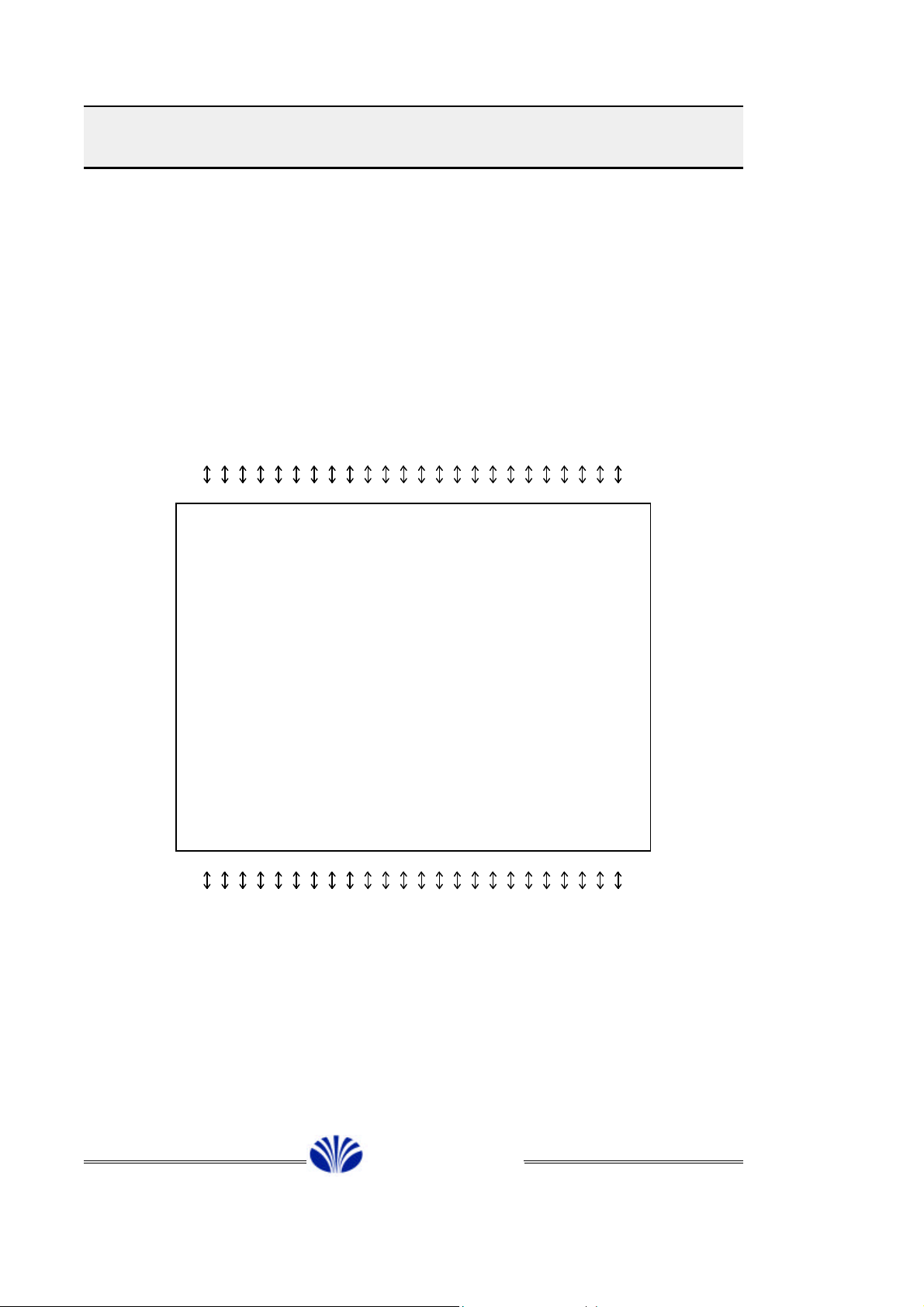
2. DMC73C168 BLOCK DIAGRAM
3. PIN ASSIGNMENT AND DESCRIPTION
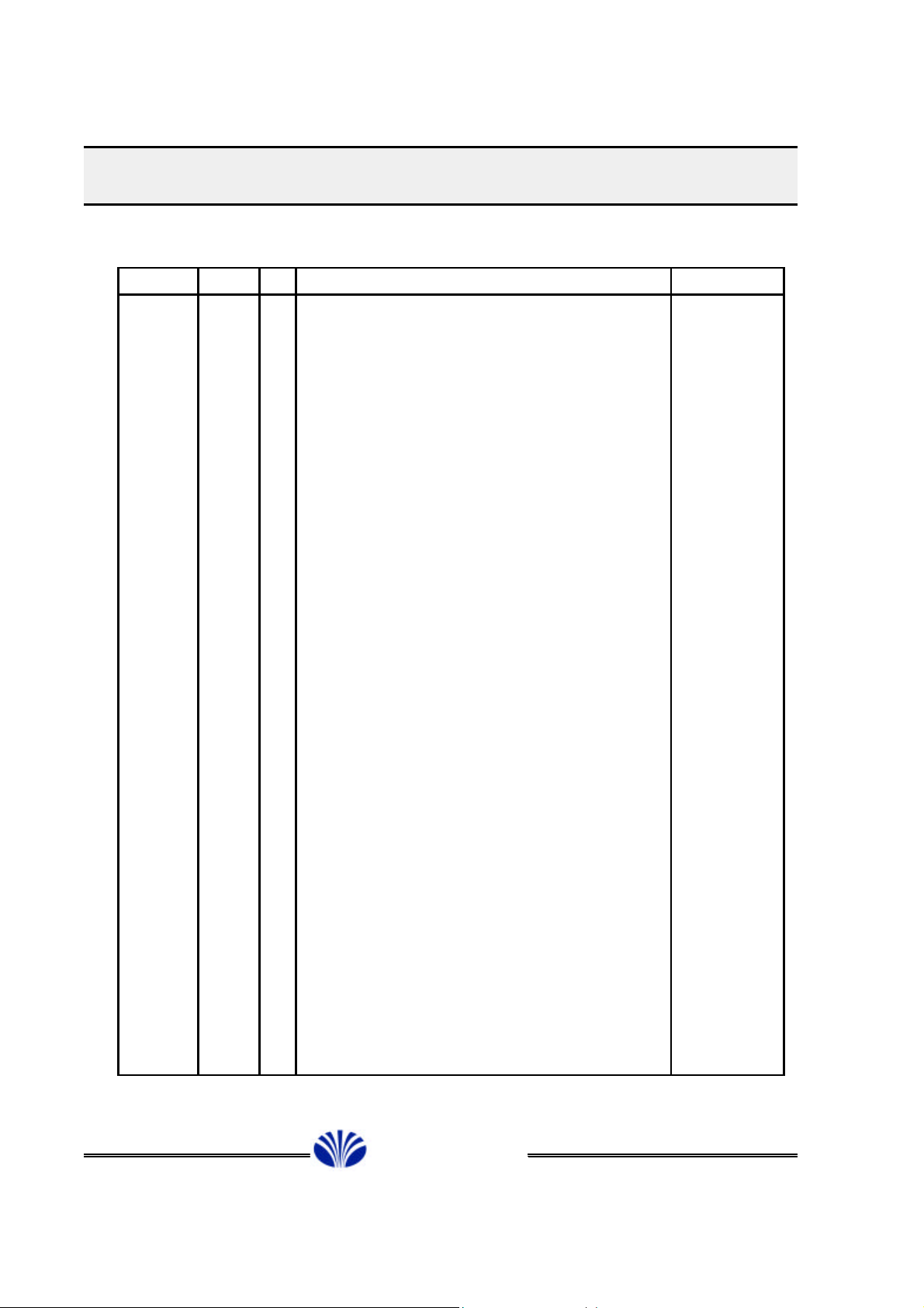
3.1 DMC73C168 Pin Assignment
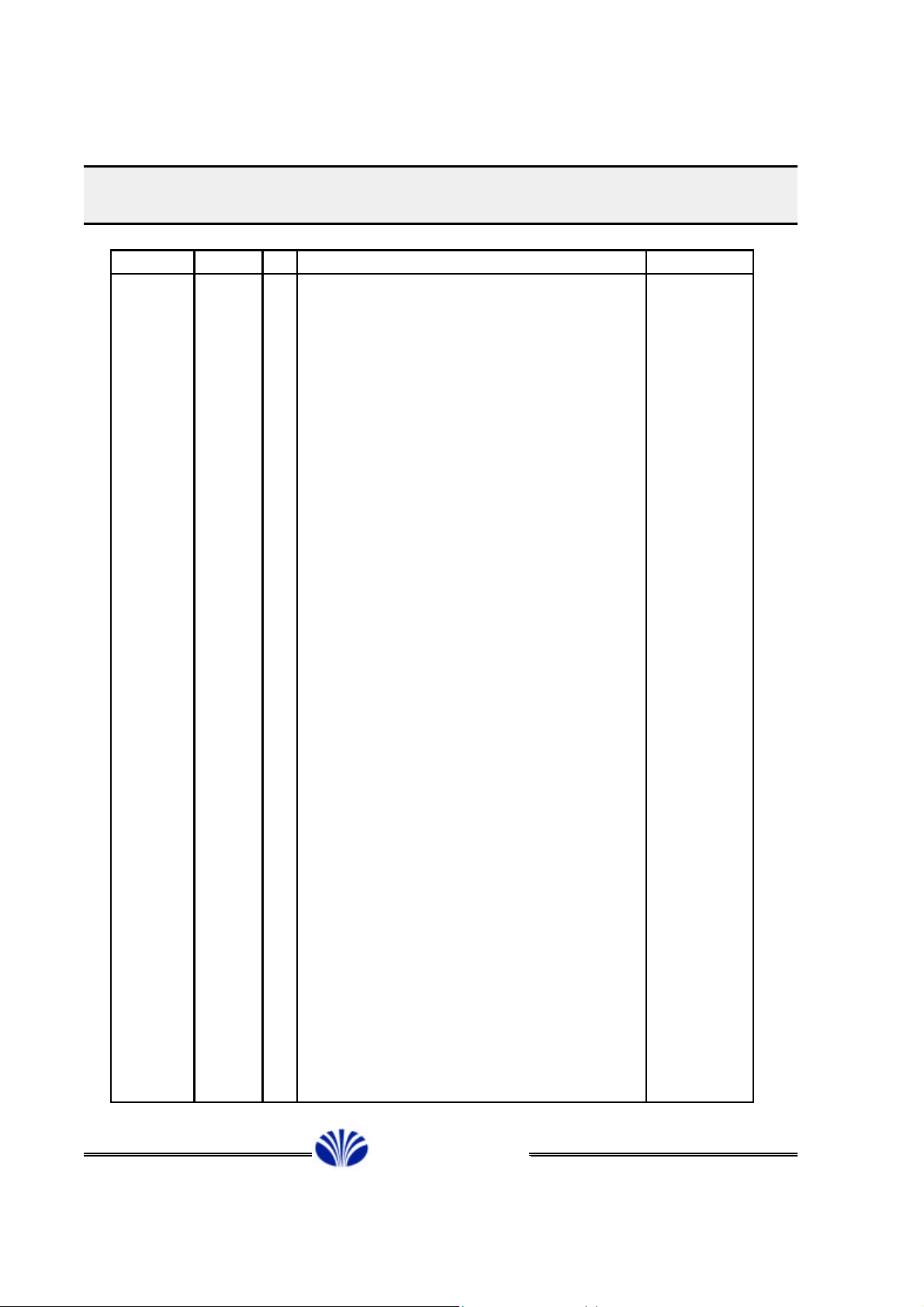
3.2 Description
4. ARCHITECTURE
4.1 Register File (RF)
4.2 Peripheral File (PF)
4.3 Peripheral RAM File (PRF)
4.4 Stack Pointer (SP)
4.5 Status Register (ST)
4.6 Program Counter (PC)
4.7 Peripheral File Map
4.8 Interrupt and Reset Priorities
3
3
5
6
6
8
11
12
12
12
13
13
14
14
33
5. DESCRIPTION OF EACH FUNCTION
5.1 Input / Output Ports
5.2 Device Initialization
5.3 I/O Control Register
5.4 Interrupt Logic and External Interrupt
5.5 Programmable Timer / Event Counter
5.6 A/D Converter
5.7 PLL
5.8 IF Counter
5.9 Serial Communication I/O Ports : SIO1, SIO2
6. OTP DEVICE SPECIFICATION
6.1 Pin Assignment of OTP and OTP Programming Adapter Board
£Ä£Á£Å£×£Ï£Ï
DAEWOO ELECTRONICS CO., LTD.
34
34
36
36
38
41
47
51
59
63
66
66

2
8Bit Single Chip Microcontroller DMC73C168
7. ELECTRICAL SPECIFICATION
7.1 Absolute Maximum Ratings Over Operating Free-Air Temperature Range
7.2 Recommended Operating Conditions
7.3 Electrical Characteristics Over Full Range of Operation
7.4 AC Characteristics for Input/Output Ports
7.5 A/D Converter Characteristics
7.6 AC Characteristics for Serial I/O Ports
7.7 Schematic of Input/Outputs
7.8 80 Pin Quad Flat Package (Mechanical Data)
* APPENDICES
A. DMC73C168 Table
B. Development Support
C. OTP Programming
67
67
68
69
70
71
71
72
73
75
75
79
£Ä£Á£Å£×£Ï£Ï
DAEWOO ELECTRONICS CO., LTD.

3
8Bit Single Chip Microcontroller
1. INTRODUCTION
The DMC73C168 is an 8-Bit microcontroller that contains Prescaler, PLL Frequency Synthesizer
and 2 channel A/D converter for Digital Tuning System.
The device is provided with abundant I/O ports and 2 channel serial interface ports (SI/O) controlled
by powerful instruction. The package is 80-pin QFP and high performance CPU and internal peripheral
allow flexible and easy system design in car-stereo, radio tuner and Hi-Fi audio system.
1.1 Key Features
CMOS Technology
n
Memory Configuration
n
l 256 Byte On-Chip RAM Register file plus 128 Byte Peripheral Free RAM
Memory-Mapped Ports for Easy Addressing
l
16K-Byte On-Chip ROM
l
On-Chip PLL Frequency Synthesizer with Dual Modules Prescaler
n
Independant Frequency input ports : Max 150MHz at FM, 40MHz at AM
l
Two Types of Frequency Dividing Method : Pulse Swallow and Direct
l
8 Kinds of reference Frequencies : 1, 5, 6.25, 9, 10, 12.5, 25 and 50KHz
l
n 2 Channel SIO port
2 Channel On-Chip Timer
n
16-Bit with 5-Bit Prescaler and 16-Bit capture latch, timer outputs
l
Internal interrupt with Automatic timer Reload
l
On-Chip A/D Converter
n
2-channels with 8 bit resolution
l
Ratiometric Conversion
l
l 144 Machine-Cycles Conversion time (64us)
On-Chip IF Counter
n
17-Bit, Gate Time : Program can select from 1ms to 15ms
l
maximum Input Frequency : FM IF = 20MHz, AM IF = 5MHz
l
Easy Interrupt Handling
n
External Interrupts with Schmitt-Trigger Input
l
Software Calls through Interrupt Vectors
l
l Software Monitoring of Interrupt Status
DMC73C168
Precise Interrupt Timing through Capture Latch
l
Selectable Beep clock : 417Hz, 1KHz, 1.25KHz, 2.5KHz
n
64 I/O Pins
n
64 Bidirectional Pins
l
Wide Operating Range
n
Voltage(VDD) : 5V¡¾10%
l
£Ä£Á£Å£×£Ï£Ï
DAEWOO ELECTRONICS CO., LTD.

4
8Bit Single Chip Microcontroller
l Clock : 4.5MHz
l Temperature : -40 deg to 85 deg
l One Machine Execution Time : 0.44us (with 4.5MHz Crystal Oscillator)
n Low operating Current
l Halt Mode for Power Savings (Typical : 1uA at OSC stop)
l Warm-up mode for avoid unstable osc operation at the wake time from Halt mode.
The warm-up time can be adjustable by S/W.
n Package
l 80 QFP (Quad Flat Package)
n Development Support
l Evaluation Module : EVM73C00A & ADP73C168
l Assembler/Linker Cross Support for Popular Hosts
DMC73C168
£Ä£Á£Å£×£Ï£Ï
DAEWOO ELECTRONICS CO., LTD.
5
8Bit Single Chip Microcontroller
2. DMC73C168 BLOCK DIAGRAM
INT4-0 ¡ê A0/FMIF
RESET ¡ê A1/AMIF
Interrupt
CE ¡ê A3/AD2
(INT1) INT4-1 ¡ê A4/ECI1
VDD ¡æ ¡ê E1/SI1
VSS ¡æ ¡ê E3/SO2
OSCIN ¡ê B0/T1OUT
OSCOUT
Control
RAM
384 Byte
8 BIT
CPU
Peripheral
/Memory
Control
OSC
GEN
INT3 ¡ê A2/AD1
INT2 ¡ê A6/INT4
INT6 ¡ê E0/SO1
INT5 ¡ê E2/SCLK1
INT7 ¡ê E4/SI2
EXT INT4
EXT INT3
A/D CON
TIMER1
TIMER2
SIO 1
SIO 2
PORT A
¡ê A5/ECI2
BEEP GEN
¡ê A7/INT3
PORT E
¡ê E5/SCLK2
¡ê E6
¡ê E7/BEEP
PORT B
¡ê B1/T2OUT
DMC73C168
ROM
Loop
16 Kbyte
PORT B
PORT C
PORT D
PORT F
PORT GPORT H
¡ê B2-B7
¡ê C0-C7
¡ê D0-D7
TEST ¡æ
EO1 ¡ç
EO2 ¡ç
VCOL ¡æ
VCOH ¡æ
VREF ¡æ
VASS ¡æ ¡ê F0-F7
Phase Locked
H0-H7 ¡ê ¡ê G0-G7
£Ä£Á£Å£×£Ï£Ï
DAEWOO ELECTRONICS CO., LTD.
6
£Ä£Á£Å£×£Ï£Ï
8Bit Single Chip Microcontroller DMC73C168
3. PIN ASSIGNMENT AND DESCRIPTION
3.1 DMC73C168 Pin Assignment
B B
1 0
/ /
T T
2 1
O O
C C C D D D D D D D D B B B B B B U U H H H H H
2 1 0 7 6 5 4 3 2 1 0 7 6 5 4 3 2 T T 7 6 5 4 3
64 41
C3 ¡ê 65 ¡ê H2
C4 ¡ê ¡ê H1
C5 ¡ê ¡ê H0
C6 ¡ê ¡ê G7
C7 ¡ê ¡ê G6
NC ¡ª ¡ê G5
EO1 ¡ç ¡ê G4
EO2 ¡ç ¡ê G3
VSS ¡ª ¡ê G2
VASS ¡ª ¡ê G1
VCOH ¡æ ¡ê G0
VCOL ¡æ ¡ç TEST
VREF ¡æ ¡ç VDD
NC ¡ª ¡æ OSCOUT
CE/INT1 ¡æ ¡ç OSCIN
RESET ¡æ 80 25 ¡ª VSS
* 1 24
80 PIN QFP TOP VIEW
DMC73C168
A A A A A A A A E E E E E E E E F F F F F F F F
0 1 2 3 4 5 6 7 0 1 2 3 4 5 6 7 0 1 2 3 4 5 6 7
/ / / / / / / / / / / / / / /
F A A A E E I I S S S S S S B
M M D D C C N N O I C O I C E
I I 1 2 I I T T 1 1 L 2 2 L E
F F 1 2 4 3 K K P
1 2
DAEWOO ELECTRONICS CO., LTD.

7
£Ä£Á£Å£×£Ï£Ï
8Bit Single Chip Microcontroller DMC73C168
D D D A A A A A
A A A D D D D D
T T T D D D D D
A A A R R R R R
2 1 0 7 6 5 4 3
¡é¡é¡é¡é¡é¡é¡é¡é¡é¡é¡é¡é¡é¡é¡é¡é¡é¡é¡é¡é¡é¡é¡é¡é
64 41
DATA3 ¡ê 65 ¡ê ADDR2
DATA4 ¡ê ¡ê ADDR1
DATA5 ¡ê ¡ê ADDR0
DATA6 ¡ê ¡ê
DATA7 ¡ê ¡ê
¡ª ¡ê ADDR13
¡ç ¡ê ADDR12
¡ç ¡ê ADDR11
¡ª ¡ê ADDR10
VSS ¡ª ¡ê ADDR9
¡æ ¡ê ADDR8
¡æ ¡ç VPP
VDD ¡æ ¡ç VDD
¡ª ¡æ
¡æ ¡ç VSS
VSS ¡ª 80 25 ¡ª VSS
* 1 24
80 PIN QFP TOP VIEW
OTP MODE
¡é¡é¡é¡é¡é¡é¡é¡é¡é¡é¡é¡é¡é¡é¡é¡é¡é¡é¡é¡é¡é¡é¡é¡é
X X X E E
P C O P P
G E E T T
M E E
S S
T T
H
V
DAEWOO ELECTRONICS CO., LTD.
8
£Ä£Á£Å£×£Ï£Ï
NAME
Pin No.
I/O
FUNCTIONAL DESCRIPTION
PORT TYPE
A0/FM IF
A1/AM IF
A2/AD1
A3/AD2
A6/INT4
A7/INT3
E0/SO1
E1/SI1
E3/SO2
E6
E7/BEEP
F0F1F2
F5F6F71234
789
101112
1516171819
222324
I/O
I/O
I/O
I/O
I/O
I/O
I/O
I/O
I/O
I/O
I/O
I/O
I/O
I/O
I/O
I/O
I/O
Port A is a bidirectional data port.
These Ports can be selected as universal Counter
input. A0 and A1 work as the FM IF and AM IF pin,
These Posts can be selected for an A/D Converter Input.
2 Channel/8-Bit Analog-to-Digital Converter are used for
Reference Voltage of the A/D Converter is the same
These Ports can be used as external interrupt pin.
Port E is a bidirectional data port.
These Ports can be selected as serial interface (SIO) 1.
serial clock pin, respectively.
These Ports can be selected as serial interface (SIO) 2.
The E7 Port can be used as BEEP output pin.
Port F is a bidirectional data port.
Analog-IN or
Logic-IN/
Push-Pull OUT
Analog-IN or
Logic-IN/
Logic-IN or
Schmitt-
Push-Pull OUT
Logic-IN/
Logic-IN/
Push-Pull OUT
8Bit Single Chip Microcontroller DMC73C168
3.2 Description
3.2 Description
independently. The maximum input frequency is 5MHz
independently. The maximum input frequency is 5MHz
for AM IF (0.1Vp-p) and 20MHz (0.1Vp-p) for FM IF.
for AM IF (0.1Vp-p) and 20MHz (0.1Vp-p) for FM IF.
A4/ECI1
A4/ECI1
A5/ECI2
A5/ECI2
E2/SCLK1
E2/SCLK1
E4/SI2
E4/SI2
E5/SCLK2
E5/SCLK2
13
13
14
14
the Sequential Comparison method by program.
the Sequential Comparison method by program.
level of VDD (5V¡¾10%)
level of VDD (5V¡¾10%)
5
I/O
5
6
6
The A4,A5 Port can be used as event counter input 1,2.
I/O
The A4,A5 Port can be used as event counter input 1,2.
I/O
I/O
I/O
E0, E1 and E2 work as the serial output, serial input and
I/O
E0, E1 and E2 work as the serial output, serial input and
I/O
E3, E4 and E5 work as the serial output, serial input and
I/O
E3, E4 and E5 work as the serial output, serial input and
I/O
serial clock pin, respectively.
I/O
serial clock pin, respectively.
Push-Pull OUT
Push-Pull OUT
Trigger-IN/
Trigger-IN/
Push-Pull OUT
Push-Pull OUT
Logic-IN/
Logic-IN/
Push-Pull OUT
Push-Pull OUT
F3
F3
F4
F4
20
20
21
21
I/O
I/O
I/O
I/O
DAEWOO ELECTRONICS CO., LTD.
DAEWOO ELECTRONICS CO., LTD.
9
NAME
PIN NO.
I/O
FUNCTION DESCRIPTION
PORT TYPE
G0G1G2G3G4G5G6G7H0H1H2H3H4H5H6
H7
B0/T1OUT
B1/T2OUT
B2
B3B4B5B6B7D0D1D2D3D4D5D6D7C0C1C2C3C4C5C6C7303132333435
3637383940414243444546
4748495051525354555657585960616263646566676869
I/O
I/O
I/O
I/O
I/O
I/O
I/O
I/O
I/O
I/O
I/O
I/O
I/O
I/O
I/O
I/O
I/O
I/O
I/O
I/O
I/O
I/O
I/O
I/O
I/O
I/O
I/O
I/O
I/O
I/O
I/O
I/O
I/O
I/O
I/O
I/O
I/O
I/O
I/O
I/O
Port G is a bidirectional data port.
Port H is a bidirectional data port.
Port B is a bidirectional data port.
Port B0, B1 can be selected as Timer 1 & 2 output ports.
Port D is a bidirectional data port.
Port C is a bidirectional data port.
Logic-IN/
Push-Pull OUT
Logic-IN/
Push-Pull OUT
Logic-IN/
Push-Pull OUT
Logic-IN/
Push-Pull OUT
Logic-IN/
Push-Pull OUT
£Ä£Á£Å£×£Ï£Ï
NAME
PIN NO.
I/O
FUNCTION DESCRIPTION
PORT TYPE
G0G1G2G3G4G5G6G7H0H1H2H3H4H5H6
H7
B0/T1OUT
B1/T2OUT
B2
B3B4B5B6B7D0D1D2D3D4D5D6D7C0C1C2C3C4C5C6C7303132333435
3637383940414243444546
4748495051525354555657585960616263646566676869
I/O
I/O
I/O
I/O
I/O
I/O
I/O
I/O
I/O
I/O
I/O
I/O
I/O
I/O
I/O
I/O
I/O
I/O
I/O
I/O
I/O
I/O
I/O
I/O
I/O
I/O
I/O
I/O
I/O
I/O
I/O
I/O
I/O
I/O
I/O
I/O
I/O
I/O
I/O
I/O
Port G is a bidirectional data port.
Port H is a bidirectional data port.
Port B is a bidirectional data port.
Port B0, B1 can be selected as Timer 1 & 2 output ports.
Port D is a bidirectional data port.
Port C is a bidirectional data port.
Logic-IN/
Push-Pull OUT
Logic-IN/
Push-Pull OUT
Logic-IN/
Push-Pull OUT
Logic-IN/
Push-Pull OUT
Logic-IN/
Push-Pull OUT
£Ä£Á£Å£×£Ï£Ï
8Bit Single Chip Microcontroller DMC73C168
DAEWOO ELECTRONICS CO., LTD.
DAEWOO ELECTRONICS CO., LTD.
10
NAME
Pin No.
I/O
FUNCTION DESCRIPTION
PORT TYPE
VCOL
EO1
VSS
OSCIN
76
71
73, 25
26II
O
I
with 0.3Vp-p minimum.
AM VCO input port.
This terminal can be selected by direct-dividing method
in pulse-swallow method, the range of local oscillator
REF
power for analog circuit in the device.
Phase comparison error output ports.
output signal is logic high level. If divided frequency is
lower than the reference frequency, output signal is vice
Ground reference
Connect 4.5MHz Crystal.
Analog-IN
3-State-OUT
£Ä£Á£Å£×£Ï£Ï
8Bit Single Chip Microcontroller DMC73C168
VCOH
VCOH
VDD
VDD
VREF
VREF
NC
NC
75
75
28
28
77
77
70
70
FM VCO input port.
FM VCO input port.
Only Pulse swallow method is used for this port.
Only Pulse swallow method is used for this port.
The range of local oscillator output is 10MHz to 150MHz
The range of local oscillator output is 10MHz to 150MHz
The output is required by capacitor coupling because an
The output is required by capacitor coupling because an
AC amplifier is contained.
AC amplifier is contained.
or pulse-swallow method.
or pulse-swallow method.
In direct-dividing method, the range of local oscillator
In direct-dividing method, the range of local oscillator
output is 0.5MHz to 10MHz with 0.3Vp-p minimum, and
output is 0.5MHz to 10MHz with 0.3Vp-p minimum, and
output is 5MHz to 40MHz with 0.3Vp-p minimum.
output is 5MHz to 40MHz with 0.3Vp-p minimum.
Input to this port should be coupled by capacitor coupling
Input to this port should be coupled by capacitor coupling
because and AC amplifier is contained.
because and AC amplifier is contained.
Power source port.
Power source port.
The terminal supplies 5V¡¾10% for normal operation.
The terminal supplies 5V¡¾10% for normal operation.
VDD and VREF must be connected to the same electric
VDD and VREF must be connected to the same electric
potential. VDD is a power for logic circuit and V
potential. VDD is a power for logic circuit and V
No connection
No connection
is a
is a
Analog-IN
Analog-IN
EO2
EO2
TEST
TEST
VASS
VASS
OSCOUT
OSCOUT
72
72
29
29
74
74
27
27
O
The divided frequency of VCO output and the reference
O
The divided frequency of VCO output and the reference
frequency are compared in their phase.
frequency are compared in their phase.
If divided frequency is higher than the reference frequency,
If divided frequency is higher than the reference frequency,
versa. When two frequencies are matched, port become a
versa. When two frequencies are matched, port become a
floating state.
floating state.
EO1 and EO2 have the same waveform.
EO1 and EO2 have the same waveform.
I
Internal Chip Test port.
I
Internal Chip Test port.
It should be connected to VSS.
It should be connected to VSS.
VSS is a ground for logic circuit and VASS is a ground for
VSS is a ground for logic circuit and VASS is a ground for
Analog circuit in the device
Analog circuit in the device
O
Crystal oscillator input and output ports.
O
Crystal oscillator input and output ports.
DAEWOO ELECTRONICS CO., LTD.
DAEWOO ELECTRONICS CO., LTD.
11
NC
RESET
CE/INT1
788079II
No connection
System reset request input port.
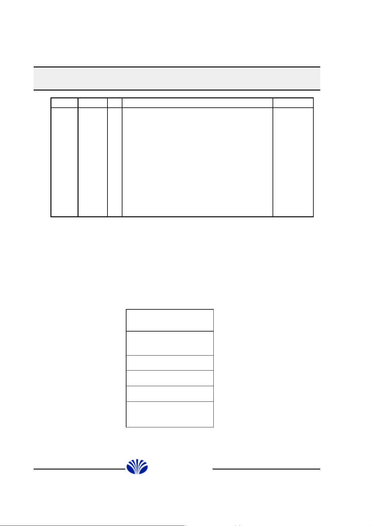
The reset pin must be held low for minimum of 5 internal
clock cycles to guarantee recognition by the device.
Device selection Signal input port.
External interrupt input port.
When activated, CPU resumes its operation from HALT
mode
Schimitt-
Trigger-IN
£Ä£Á£Å£×£Ï£Ï
8Bit Single Chip Microcontroller DMC73C168
NAME PIN NO. I/O FUNCTION DESCRIPTION PORT TYPE
NAME PIN NO. I/O FUNCTION DESCRIPTION PORT TYPE
The device initialization requires 15 machine cycles.
The device initialization requires 15 machine cycles.
This port can be used as a Chip Enable input.
This port can be used as a Chip Enable input.
4. ARCHITECTURE
4. ARCHITECTURE
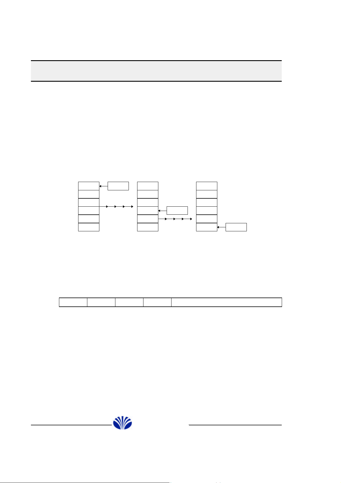
The DMC73C168 has a maximum memory address space of 64K bytes and only the Single-Chip mode.
The DMC73C168 has a maximum memory address space of 64K bytes and only the Single-Chip mode.
On-Chip memory spaces are configured as shown in Table 4.1.
On-Chip memory spaces are configured as shown in Table 4.1.
In the sections that follow, the Register File (RF) and the Peripheral File (PF) are described along
In the sections that follow, the Register File (RF) and the Peripheral File (PF) are described along
with three important registers in the CPU : the Stack Pointer (SP), the Status Register (ST), and the
with three important registers in the CPU : the Stack Pointer (SP), the Status Register (ST), and the
Program Counter (PC)
Program Counter (PC)
Memory Address
> 0000
> 0000
Register File (RF)
> 00FF
> 00FF
> 0132
> 0132
> 013F
> 013F
> 01BF
> 01BF
> C005
> C005
Register File (RF)
Peripheral File (PF)
Peripheral File (PF)
Reserved
Reserved
128 byte PRF
128 byte PRF
Not Available
Not Available
16K bytes ROM
16K bytes ROM
> 0100
> 0100
> 0133
> 0133
> 0140
> 0140
> 01C0
> 01C0
> C006
> C006
; 256 byte RAM
; 128 byte RAM
; 128 byte RAM
> FFFF
> FFFF
Table 4-1. DMC73C168 Memory Map
DAEWOO ELECTRONICS CO., LTD.
DAEWOO ELECTRONICS CO., LTD.

12
8Bit Single Chip Microcontroller DMC73C168
4.1 Register File (RF)
The 256-byte on chip RAM resides in location >0000 to >00FF (‘>’ means hex) of the DMC73C168’s
address space and is called the Register File (RF). The RAM is treated as registers by much of the
instruction set and numbered R0-R255. The first two registers, R0 and R1, are also called the A and
B registers respectively. Several instructions specify A or B as either the source or destination
register ; e.g., STSP stores the contents of the Stack Pointer (SP) in the B register.
Except where stated otherwise, any register in the Register File can be addressed as an 8-bit source or
destination register. The stack is also located in the Register File. Refer to section 4.3 for information
regarding the initialization of the Stack Pointer (SP) and stack definition in the Register File.
4.2 Peripheral File (PF)
The Peripheral File (PF) resides in location >0100 to >0132 of the DMC73C168’s address space.
Peripheral File locations are numbered P0-P50. The PF registers are used for interrupt control, parallel
I/O, timer control, PLL, IF counter, BEEP, SIO and A/D converter control.
4.3 Peripheral RAM File (PRF)
The Peripheral RAM file (PRF) resides in location >0140 to >01BF of DMC73C168’s address space.
PRF will act a role P64-P191. Useage is for additional RAM, but addressing method is same as
Peripheral File’s.
Memory address
>0100
>0132
>0133
>013F
>0140
>01BF
>01C0
>01FF
Table 4.3 DMC73C168 Peripheral File Map
P0
:
P50
P51
:
P63
P64
:
P191
P192
:
P255
Peripheral File
Not Avail
128 bytes PRF
Not Avail
£Ä£Á£Å£×£Ï£Ï
DAEWOO ELECTRONICS CO., LTD.
13
£Ä£Á£Å£×£Ï£Ï
8Bit Single Chip Microcontroller DMC73C168
4.4 Stack Pointer (SP)
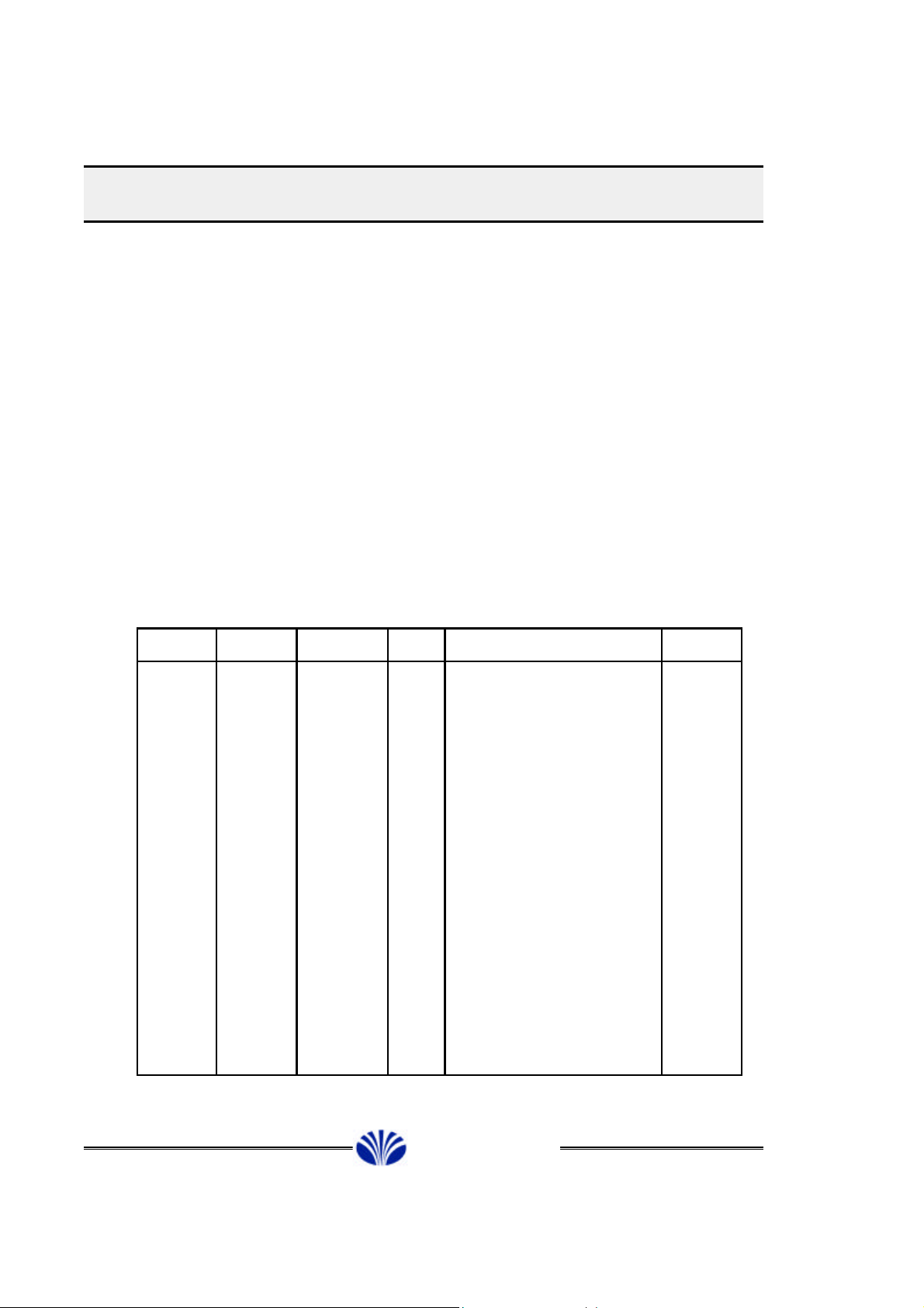
The Stack Pointer(SP) is an 8-bit register in the CPU that is typically used to hold a pointer in RAM
(the Register File). However, the SP can also be used as temporary data storage if a stack is not
implemented, or if the SP contents are not needed. When a stack is implemented just before data is
pushed onto the stack and automatically decremented immediately after data is poped from the
stack. Upon assertion if the RESET function (see Section 4.7) >01 is loaded into the SP. The size
of the stack can be changed from the 254-level stack at RESET to a smaller stack by executing
a stack initialization program as illustrated in Figure 4.4. The This feature allows the stack to be
located anywhere in the Register File. The SP is initialized through the B register (R1).
RFRF
PCH
PCL
>0001
>0002
>0003
>0004
>0005
>0006
RF
Figure 4.4 Example of Stack Initialization in the Register File
SP
>01
Interrupt
ST
PCH
PCL
SP
>04
CALL
4.5 Status Register (ST)
The Status Register (ST) is an 8-bit register in the CPU that contains three conditional status bits ;
Carry (C), Sign (N), Zero (Z), and a global Interrupt Enable bit (I) as shown in Figure 4-5.
Bit
7 6 5 4 3 2 1 0
C N Z I FUTURE USE
C : CARRY OUT
N : SIGN
Z : ZERO
I : INTERRUPT ENABLE
SP
>06
The C, N and Z bits are used mostly for arithmetic operations, bit rotating, and conditional branching.
The Carry(C) bits is used as the carry-in and carry-out for most of lotate and arithmetic instructions.
The Sign(N) bit contains the most significant bit of the destination operand contents after instruction
execution. The Zero(Z) bit contains a one when all bits of the destination operand are equal to zero
after instruction execution. The C, N and Z status bits also have jump-on-condition instructions
associated them. The global Interrupt Enable (I) bit must be set to one by the EINT instruction in
Figure 4-5. Status Register (ST)
DAEWOO ELECTRONICS CO., LTD.
14
REGISTER
ADDRESS
NAME
NOTE
FUNCTION
RESET
VALUEP0P1P2P4P5P6
P7P8P9
P10
P11
P13
P14
P15
P16
>0100
>0101
>0102
>0104
>0105
>0106
>0117
>0118
>0109
>010A
>010B
>010D
>010E
>010F
>0110
IOCTL0
IOCTL1
IOCTL2
T1MSDATA
T1LSDATA
T1CTL0
T1CTL1
T2MSDATA
T2LSDATA
T2CTL0
T2CTL1
APSLCT
ADCTL
ADDATA
PLLCTL0
1111111111111
Interrupt 1,2 and 3 control register
Ext-INT 1,3 and 4 input edge select
Interrupt 4,5,6,7 control register
Timer 1 MSB reload register
/ MSB readout latch
Timer 1 LSB reload register
/ LSB decrementer value
Timer 1 control register 0
/ MSB readout latch
Timer 1 control register 1
/ LSB capture latch value
Timer 2 MSB reload register
/ MSB readout latch
Timer 2 LSB reload register
/ LSB decrementer value
Timer 2 control register 0
/ MSB readout latch
Timer 2 control register 1
/ LSB capture latch value
A port select control register
A/D converter control register
A/D converter data value
PLL control register 0
00000000
0000x000
00000000
xxxxxxxx
xxxxxxxx
x0xxxxxx
0x0xxxxx
xxxxxxxx
xxxxxxxx
00xxxxxx
0x0xxxxx
00000000
00xxxxx0
00000000
00000000
£Ä£Á£Å£×£Ï£Ï
8Bit Single Chip Microcontroller DMC73C168
order for any of the individual interrupts (INTn) to be recognized by the CPU. The Interrupt Enable
(I) bit can cleared by DINT instruction of by executing a device RESET (see Section 4.7).
4.6 Program Counter (PC)
The DMC73C168’s 16-bit Program Counter (PC) consists of two 8-bit registers in the CPU which
contain the MSB and the LSB respectively of a 16-bit address ; the Program Counter High (PCH) and
Low (PCL). The PC acts as the 16-bit address pointer of the opcodes and operands in memory of the
currently executing instruction. Upon assertion of the RESET function, the MSB and the LSB of the PC
are loaded into the A and B registers of the Register File (see Section 4.7).
4.7 Peripheral File Map
The Peripheral File (PF) resides in locations >0100 to >01BF of the DMC73C168’s address space as
shown in Table 4.7
Table 4.7 Peripheral File Map
DAEWOO ELECTRONICS CO., LTD.
15
REGISTER
ADDRESS
NAME
NOTE
FUNCTION
RESET
VALUE
P17
P18
P19
P22
P23
P24
P25
P27
P28
P29
P30
P32
P33
P34
P35
P36
P37
P38
P39
P40
P41
P42
P43
P44
P45
P46
P47
P50
>0111
>0112
>0113
>0116
>0117
>0118
>0119
>011B
>011C
>011D
>011E
>0120
>0121
>0122
>0123
>0124
>0125
>0126
>0127
>0128
>0129
>012A
>012B
>012C
>012D
>012E
>012F
>0132
PLLCTL1
PLLDATAH
PLLDATAL
IFCCTL
IFCLSD
IFCMSD
IFCHSD
SIO1CTL
SIO1BUF
SIO2CTL
SIO2BUF
ADATA
ADDR
BDATA
BDDR
CDATA
CDDR
DDATA
DDDR
EDATA
EDDR
FDATA
FDDR
GDATA
GDDR
HDATA
HDDR
BEEP
11111
PLL control register 1
PLL program counter MSB data register
PLL program counter LSB data register
IF counter data register
IF counter data register (LSB)
IF counter data register
IF counter data register (MSB)
SIO 1 control register
SIO 1 data register
SIO 2 control register
SIO 2 data register
Port A data value
Port A direction register
Port B data value
Port B direction
Port C data value
Port C direction register
Port D data value
Port D direction register
Port E data value
Port E direction register
Port F data value
Port F direction register
Port G data value
Port G direction register
Port H data value
Port H direction register
BEEP control register
0xxx0000
00000000
00000000
00000000
00000000
00000000
xxxxxxx0
0000000x
xxxxxxxx
0000000x
xxxxxxxx
xxxxxxxx
00000000
xxxxxxxx
00000000
xxxxxxxx
00000000
xxxxxxxx
00000000
xxxxxxxx
00000000
xxxxxxxx
00000000
xxxxxxxx
00000000
xxxxxxxx
00000000
00000000
P64::
P191
>0140::
>01BF
Peripheral RAM
128 bytes
xxxxxxxx
xxxxxxxx
£Ä£Á£Å£×£Ï£Ï
8Bit Single Chip Microcontroller DMC73C168
Notes 1 : Be careful when using logical instructions (e.g., ANDP, ORP, XORP) on these registers
because of different read/write functions.
2 : ‘x’ means indeterminate
3 : P3, P12, P20, P21, P26,P31, P48, P49, P51-63 are not implemented.
DAEWOO ELECTRONICS CO., LTD.
16
R/W
BIT 7
BIT 6
BIT 5
BIT 4
BIT 3
BIT 2
BIT 1
BIT 0
READ
INT3F
INT3E
INT2F
INT2E
INT1F
INT1E
P0
>0100
WRITE
NOT USED
INT3C
INT3E
INT2C
INT2E
INT1C
INT1E
RESET VALUE
XXOOOOO
O
R/W
BIT 7
BIT 6
BIT 5
BIT 4
BIT 3
BIT 2
BIT 1
BIT 0
READ
P1
>0101
WRITE
RESET VALUE
R/W
BIT 7
BIT 6
BIT 5
BIT 4
BIT 3
BIT 2
BIT 1
BIT 0
READ
INT7F
INT7E
INT6F
INT6E
INT5F
INT5E
INT4F
INT4E
P2
>0102
WRITE
INT7C
INT7E
INT6C
INT6E
INT5C
INT5E
X
INT4E
RESET VALUE
OOOOOOO
O
£Ä£Á£Å£×£Ï£Ï
8Bit Single Chip Microcontroller DMC73C168
4.7.1 Peripheral Files detail Description
1)
I/O CONTROL REGISTERS
PF NAME : IOCTL0 : I/O CONTROL REGISTER 0
X = Indeterminate
Read : INTnF : 0 = INTn inactive Write : INTnE :0 = INTn disable
1 = INTn pending 1 = INTn enable
INTnC :0 = No Effect
1 = Clear INTn flag
PF NAME : IOCTL1 : I/O CONTROL REGISTER 1
INT41F INT41E INT40F INT40E INT40S INT3S INT1S
INT41C INT41E INT40C INT40E
O O O O X O O O
NOT
USED
INT40S INT3S INT1S
X = Indeterminate
INT41 = INT4-1
INT40 = INT4-0
Read : INTnF : 0 = INTn inactive Write : INTnE :0 = INTn disable
1 = INTn pending 1 = INTn enable
INTnS :0 = Falling edge sensing INTnC :0 = No Effect
1 = Rising edgi sensing 1 = Clear INTn flag
PF NAME : IOCTL2 : I/O CONTROL REGISTER 2
Read : INTnF : 0 = INTn inactive Write : INTnE :0 = INTn disable
1 = INTn pending 1 = INTn enable
This bit is automatically cleared INTnC :0 = No Effect
When CPU fetch its vector address. 1 = Clear INTn flag
<< INT4F is not automatically cleared
When CPU fetch vector address>>
DAEWOO ELECTRONICS CO., LTD.
17
R/W
BIT 7
BIT 6
BIT 5
BIT 4
BIT 3
BIT 2
BIT 1
BIT 0
READ
MSB READOUT LATCH
P4
>0104
WRITE
MSB READOUT LATCH
RESET VALUE
XXXXXXX
X
R/W
BIT 7
BIT 6
BIT 5
BIT 4
BIT 3
BIT 2
BIT 1
BIT 0
READ
LSB DECREMENTER VALUE
P5
>0105
WRITE
LSB RELOAD REGISTER
RESET VALUE
XXXXXXX
X
R/W
BIT 7
BIT 6
BIT 5
BIT 4
BIT 3
BIT 2
BIT 1
BIT 0
READ
MSB READOUT LATCH
P6
>0106
WRITE
X
T1OUTXXXXXX
RESET VALUE
XOXXXXX
X
R/W
BIT 7
BIT 6
BIT 5
BIT 4
BIT 3
BIT 2
BIT 1
BIT 0
READ
LSB CAPTURE LATCH
P7
>0107
WRITE
RESET VALUE
OXOXXXX
X
£Ä£Á£Å£×£Ï£Ï
8Bit Single Chip Microcontroller DMC73C168
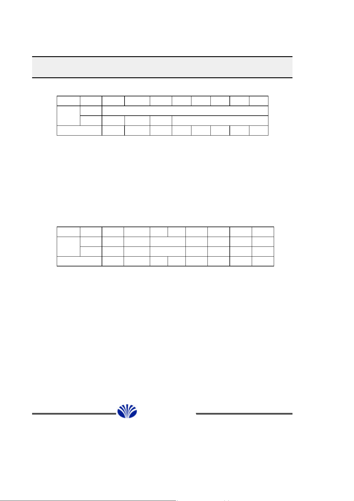
2) TIMER 1 & 2 CONTROL REGISTERS
PF NAME : T1MSDATA : TIMER 1 MS BYTE DATA REGISTER
PF NAME : T1LSDATA : TIMER 1 LS BYTE DATA REGISTER
PF NAME : T1CTL0 : TIMER 1 CONTROL REGISTER 0
T1OUT : Timer 1 toggle output enable bit.
This write bit determines PORT B0 is timer 1 toggle output pin or normal I/O pin.
0 = PORT B0 is normal I/O pin.
1 = PORT B0 is timer 1 toggle output in, and B0 is toggle when Timer 1
decrements through zero value.
PF NAME : T1CTL1 : TIMER 1 CONTROL REGISTER 1
START1 SOURC1 T1HALT PRESCALER RELOAD REGISTER (PL)
Write : SOURC1 : 0 = Internal clock source Fosc/4
1 = External clock source from A4/ECI1
START1 : 0 = Timer 1 is stop, hold current count value and clear INT2 flag.
1 = Timer 1 reloads prescaler and decrementer, begins decrementing.
T1HALT : 0 = Timer 1 remains active when execute IDLE instruction. (WAKE-UP)
1 = Timer 1 will halt when execute IDLE instruction. (HALT)
DAEWOO ELECTRONICS CO., LTD.
18
R/W
BIT 7
BIT 6
BIT 5
BIT 4
BIT 3
BIT 2
BIT 1
BIT 0
READ
MSB READOUT LATCH
P8
>0108
WRITE
MSB READOUT REGISTER
RESET VALUE
XXXXXXX
X
R/W
BIT 7
BIT 6
BIT 5
BIT 4
BIT 3
BIT 2
BIT 1
BIT 0
READ
LSB DECREMENTER VALUE
P9
>0109
WRITE
LSB RELOAD REGISTER
RESET VALUE
XXXXXXX
X
R/W
BIT 7
BIT 6
BIT 5
BIT 4
BIT 3
BIT 2
BIT 1
BIT 0
READ
MSB READOUT LATCH
P10
>010A
WRITE
CASCADE
T2OUTXXXXXX
RESET VALUE
OOXXXXX
X
£Ä£Á£Å£×£Ï£Ï
8Bit Single Chip Microcontroller DMC73C168
PF NAME : T2MSDATA : TIMER 2 MS BYTE DATA REGISTER
PF NAME : T2LSDATA : TIMER 2 LS BYTE DATA REGISTER
PF NAME : T2CTL0 : TIMER 2 CONTROL REGISTER 0
T2OUT : Timer 2 toggle output enable bit.
This write bit determines PORT B1 is timer 2 toggle output pin or normal I/O pin.
0 = PORT B1 is normal I/O pin.
1 = PORT B1 is timer 1 toggle output pin, and B1 is toggle when Timer 2
decrements through zero value.
CASCADE : Timer 2 cascade control bit
0 = Timer 2 is not cascaded with Timer 1, Timer 2 clock is determined by
source bit.
1 = Timer 1 and 2 are cascaded, clock source is generated by Timer 1 reload
pulse, overrides source bit.
DAEWOO ELECTRONICS CO., LTD.
19
INT3SEL
AMIFSEL
FMIFSEL
£Ä£Á£Å£×£Ï£Ï
8Bit Single Chip Microcontroller DMC73C168
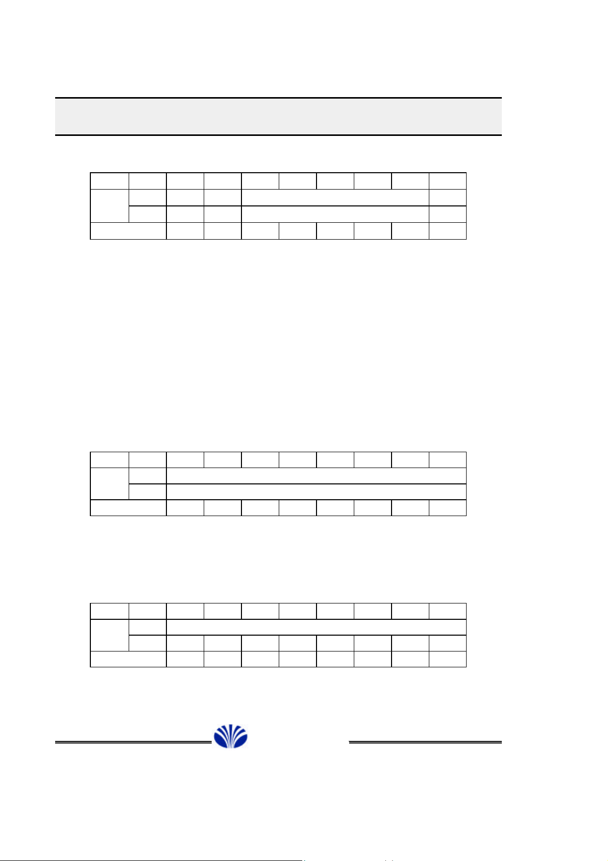
PF NAME : T2CTL1 : TIMER 2 CONTROL REGISTER 1
R/W BIT 7 BIT 6 BIT 5 BIT 4 BIT 3 BIT 2 BIT 1 BIT 0
READ LSB CAPTURE LATCHP11
>010B
RESET VALUE O X O X X X X X
Write : SOURC2 : 0 = Internal clock source Fosc/4
3) A/D CONVERTER REGISTERS
WRITE
START2 SOURC2 T2HALT PRESCALER RELOAD REGISTER (PL)
1 = External clock source from A5/ECI2
START2 : 0 = Timer 2 is stop, hold current count value and clear INT6 flag.
1 = Timer 2 reloads prescaler and decrementer, begins decrementing.
T2HALT : 0 = Timer 2 remains active when execute IDLE instruction. (WAKE-UP)
1 = Timer 2 will halt when execute IDLE instruction. (HALT)
PF NAME : APSLCT : PORT A SELECT CONTROL REGISTER
R/W BIT 7 BIT 6 BIT 5 BIT 4 BIT 3 BIT 2 BIT 1 BIT 0
P13
>010C
RESET VALUE
READ
WRITE
INT40SEL NOT USED AD2SEL AD1SEL
INT3SEL
INT40SEL NOT USED AD2SEL AD1SEL
O O O O O O O O
AMIFSEL FMIFSEL
FMIFSEL
AMIFSEL : FM and AM IF input enable bits. This read/write bits disable digital inputs
when FM and AM IF inputs are enabled.
0 = PORT A0 and A1 are normal I/O pins.
1 = PORT A0 and A1 are disabled.
AD1SEL
AD2SEL : A/D converter input enable bits. This read/write bits disable digital inputs
when A/D converter inputs when A/D converter inputs are enabled.
0 = PORT A2 and A3 are normal I/O pins.
1 = PORT A2 and A3 are disabled.
INT40SEL
INT3SEL : External interrupt 3 and 4-0 input enable bits. This read/write disable Digital
inputs when A/D converter inputs are enabled.
0 = PORT A7 and A6 are normal I/O pins.
1 = PORT A7 and A6 are disabled
DAEWOO ELECTRONICS CO., LTD.
20
READYC
£Ä£Á£Å£×£Ï£Ï
8Bit Single Chip Microcontroller DMC73C168
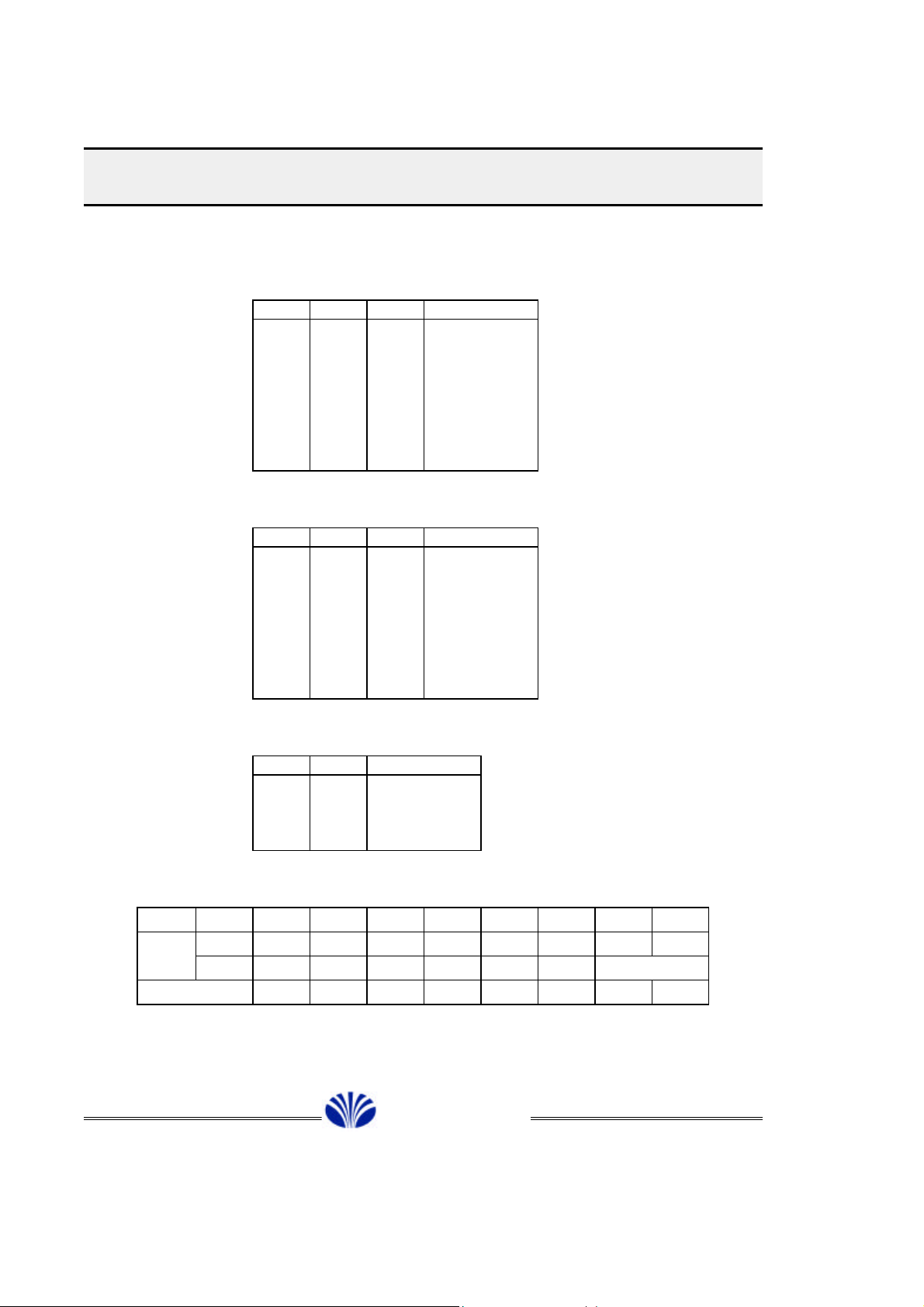
PF NAME : ADCTL : A/D CONTROL REGISTER
R/W BIT 7 BIT 6 BIT 5 BIT 4 BIT 3 BIT 2 BIT 1 BIT 0
P14 READ READY START NOT USED ADCHS
>010E WRITE READYC START NOT USED ADCHS
RESET VALUE O O X X X X X O
READ :
READY : 0 = No Operation or Incomplete Conversion
1 = Complete Conversion
WRITE
ADCHS : 0 = A/D Converter Input Channel is PORT A2
1 = A/D Converter Input Channel is PORT A3
START : 0 = Conversion Stop
1 = Conversion Start
: 0 = Ineffect
1 = Clear Ready Flag
PF NAME : ADDATA : A/D CONVERTER DATA REGISTER
R/W BIT 7 BIT 6 BIT 5 BIT 4 BIT 3 BIT 2 BIT 1 BIT 0
P15 READ CONVERSION DATA REGISTER
>010F WRITE NOT USED (INVALID)
RESET VALUE O O O O O O O O
4) PLL (PHASE LOCKED LOOP) REGISTER
PF NAME : PLLCTL0 : PLL CONTROL REGISTER 0
R/W BIT 7 BIT 6 BIT 5 BIT 4 BIT 3 BIT 2 BIT 1 BIT 0
P16 READ NOT USED
>0110 WRITE INSL1 INSL0 REF2 REF1 REF0 DTM2 DTM1 DTM0
RESET VALUE O O O O O O O O
DAEWOO ELECTRONICS CO., LTD.
21
£Ä£Á£Å£×£Ï£Ï
8Bit Single Chip Microcontroller DMC73C168
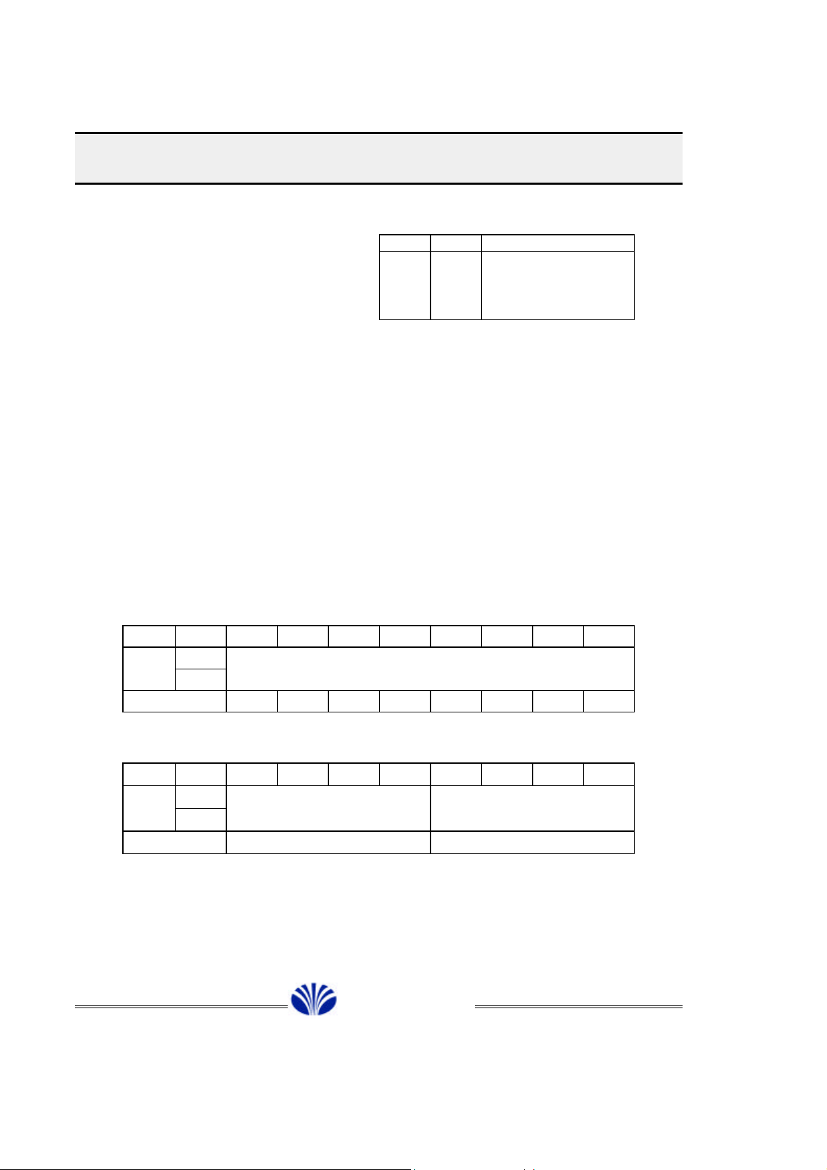
WRITE :
PHASE DETECT TIME SELECT
DTM2 DTM1 DTM0 DETECT TIME
0 0 0 0.44 us
0 0 1 0.55 us
0 1 0 0.66 us
0 1 1 0.77 us
1 0 0 0.88 us
1 0 1 1.00 us
1 1 0 1.11 us
1 1 1 1.22 us
PHASE DETECT TIME SELECT
REF2 REF1 REF0 REF. FREQ
0 0 0 1.0 KHz
0 0 1 5.0 KHz
0 1 0 6.25 KHz
0 1 1 9.0 KHz
1 0 0 10.0 KHz
1 0 1 12.5 KHz
1 1 0 25.0 KHz
1 1 1 50.0 KHz
MODE SELECT
INSL1 INSL0 INPUT MODE
0 0 NOT USED
0 1 AM DIRECT
1 0 AM SWALLOW
1 1 FM SWALLOW
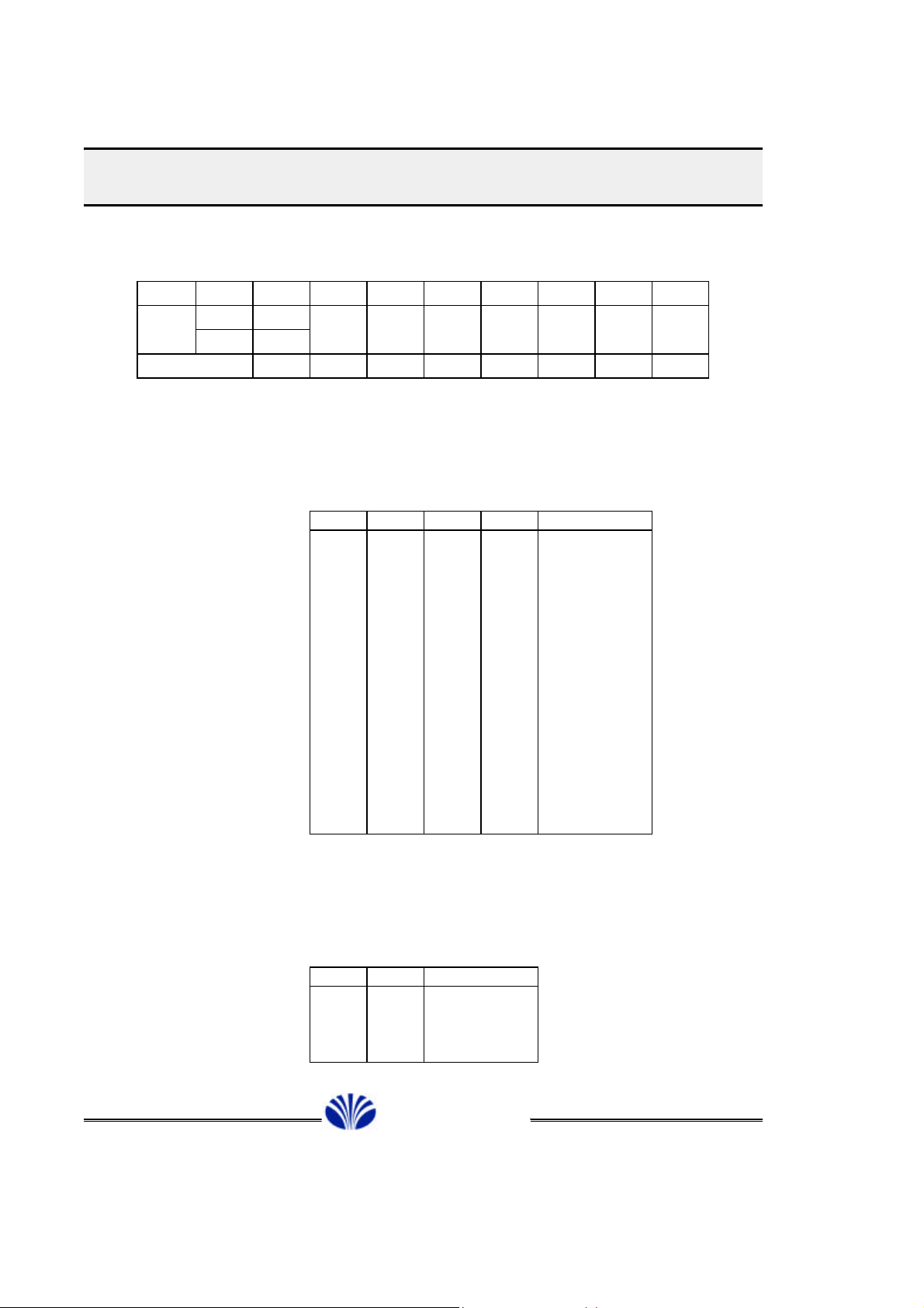
PF NAME : PLLCTL1 : PLL START/STOP CONTROL REGISTER 1
R/W BIT 7 BIT 6 BIT 5 BIT 4 BIT 3 BIT 2 BIT 1 BIT 0
P17 READ READY X X X REFTST PLLTST UL1 UL0
>0111 WRITE PLLEN X X X REFTST PLLTST NOT USED
RESET VALUE O X X X O O O O
DAEWOO ELECTRONICS CO., LTD.
22
£Ä£Á£Å£×£Ï£Ï
8Bit Single Chip Microcontroller DMC73C168
READ :
PLL UNLOCK STATUS DETECT : UL1 UL0 STATUS
0 0 PLL LOCK/STOP/OFF
0 1 REF FREQ > VCO FREQ
1 0 REF FREQ < VCO FREQ
1 1 NOT USED
READY : 0 = NO OPERATION
1 = ACTIVE
WRITE :
PLLTST : PLL TEST BIT (ATTENTION : SHOULD BE SET "0" IN NORMAL OPERATION)
0 = ACTIVE NORMAL
1 = TEST MODE
REFTST : REFERENCE DIVIDER TEST BIT(SHOULD BE SET "0" IN NORMAL OPERATION)
0 = ACTIVE NORMAL OPERATION
1 = REFERENCE TEST MODE
PLLEN : 0 = PLL OFF, PLL STOP
1 = PLL ON, PLL START
PF NAME : PLLDATAH : PLL PC MSB DATA REGISTER
R/W BIT 7 BIT 6 BIT 5 BIT 4 BIT 3 BIT 2 BIT 1 BIT 0
P18 READ PLL PC MSB DATA
>0112 WRITE
RESET VALUE O O O O O O O O
PF NAME : PLLDATAL : PLL PC LSB DATA REGISTER
R/W BIT 7 BIT 6 BIT 5 BIT 4 BIT 3 BIT 2 BIT 1 BIT 0
P19 READ PLL PC LSB DATA SWALLOW COUNTER VALUE
>0113 WRITE
RESET VALUE O O O O O O O O
DAEWOO ELECTRONICS CO., LTD.
23
£Ä£Á£Å£×£Ï£Ï
8Bit Single Chip Microcontroller DMC73C168
5) IF COUNTER REGISTER
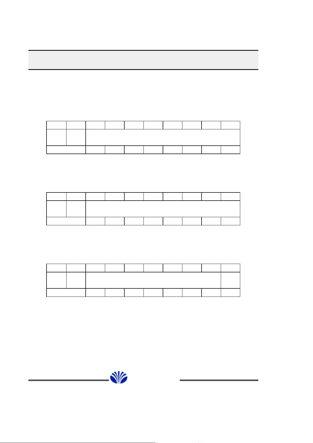
PF NAME : IFCCTL : IF CONTROL REGISTER
R/W BIT 7 BIT 6 BIT 5 BIT 4 BIT 3 BIT 2 BIT 1 BIT 0
P22 READ READY FMIF AMIF TSTIF TP3 TP2 TP1 TP0
>0116 WRITE START
RESET VALUE O O O O O O O O
READ :
READY : 0 = INACTIVE OR COMPLETE COUNTER
1 = INCOMPLETE OR ACTIVE COUNTER
WRITE :
IF FREQ. COUNTING PERIOD SELECT (TP0, TP1, TP2, TP3)
TP3 TP2 TP1 TP0 COUNT TIME
0 0 0 0 X
0 0 0 1 1 ms
0 0 1 0 2 ms
0 0 1 1 3 ms
0 1 0 0 4 ms
0 1 0 1 5 ms
0 1 1 0 6 ms
0 1 1 1 7 ms
1 0 0 0 8 ms
1 0 0 1 9 ms
1 0 1 0 10 ms
1 0 1 1 11 ms
1 1 0 0 12 ms
1 1 0 1 13 ms
1 1 1 0 14 ms
1 1 1 1 15 ms
TSTIF : IF COUNTER TEST BIT
(ATTENTION : SHOULD BE SET TO "0" IN NORMAL OPERATION)
0 = NORMAL ACTIVE MODE
1 = TEST MODE
AMIF, FMIF : IF COUNTER INPUT SELECT
FMIF AMIF COUNTING INPUT
0 0 NOT INPUT
0 1 AMIF
1 0 FMIF
1 1 X
DAEWOO ELECTRONICS CO., LTD.
24
£Ä£Á£Å£×£Ï£Ï
8Bit Single Chip Microcontroller DMC73C168
START : IF COUNTER START/STOP
0 = STOP (DISABLE)
1 = START (ENABLE)
PF NAME : IFCLSD : IF COUNTER LSB VALUE
R/W BIT 7 BIT 6 BIT 5 BIT 4 BIT 3 BIT 2 BIT 1 BIT 0
P23 READ IF COUNTER LSB VALUE
>0117
RESET VALUE O O O O O O O O
IF Counter LSB data bits
This read bits are LSB 8 bits of 17 bits IF Counter.
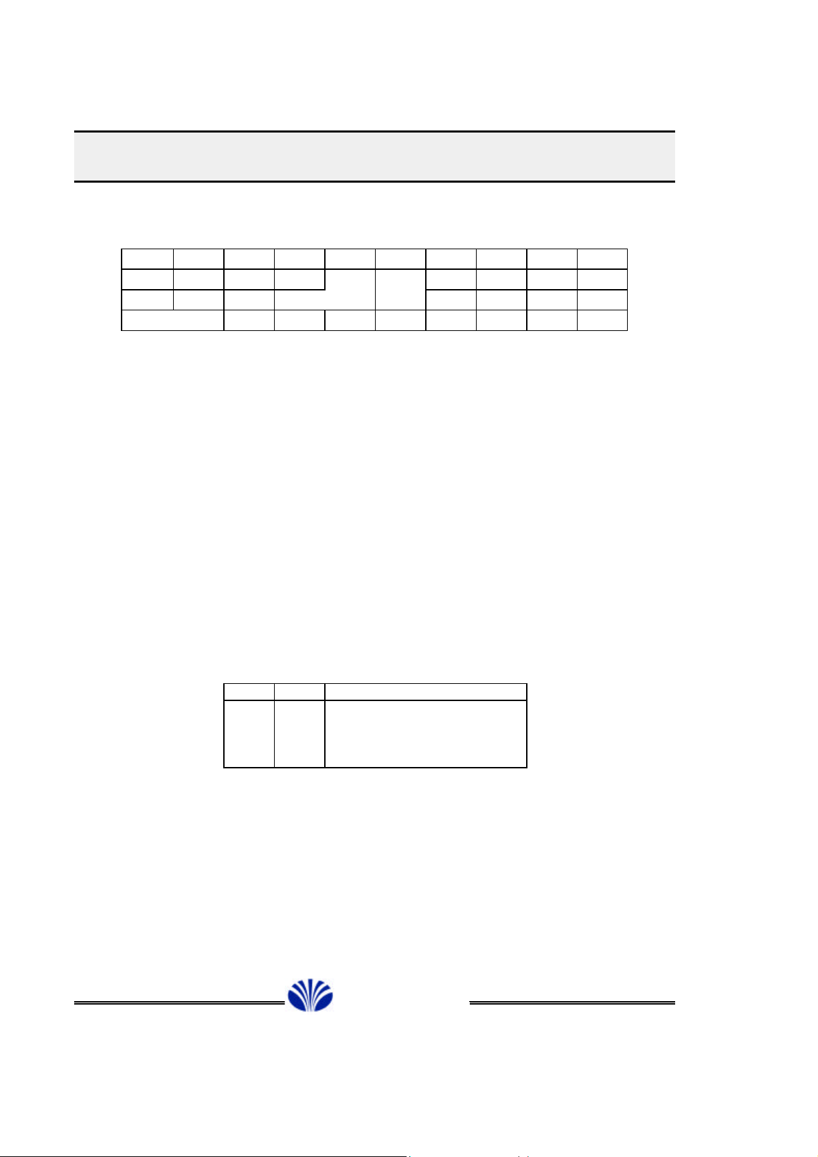
PF NAME : IFCMSD : IF COUNTER VALUE
R/W BIT 7 BIT 6 BIT 5 BIT 4 BIT 3 BIT 2 BIT 1 BIT 0
P24 READ IF COUNTER MSB-1 VALUE
>0118
RESET VALUE O O O O O O O O
IF Counter MSB data bits
This read bits are MSB 8 bits (from bit-15 to bit-8) of 17 bits IF Counter.
PF NAME : IFCHSD : IF COUNTER MSB VALUE
R/W BIT 7 BIT 6 BIT 5 BIT 4 BIT 3 BIT 2 BIT 1 BIT 0
P25 READ NOT USED IFD16
>0119
RESET VALUE X X X X X X X O
IF Counter MSB data bits
This read bits are MSB 1 bits (bit-16) of 17 bits IF Counter.
DAEWOO ELECTRONICS CO., LTD.
25
CKSRC1
£Ä£Á£Å£×£Ï£Ï
8Bit Single Chip Microcontroller DMC73C168
6) SERIAL I/O REGISTERS
PF NAME : SIO1CTL : SERIAL I/O 1 CONTROL REGISTER
R/W BIT 7 BIT 6 BIT 5 BIT 4 BIT 3 BIT 2 BIT 1 BIT 0
P27 READ SIO1AF
>011B WRITE SIO1ST CKSRC1 SIO1EC SCLK1E SO1ENA X
RESET VALUE O O O O O O O X
SIO1AF : SIO1 operation flag bit.
This read bit determines SIO1 is enabled or not.
0 = SIO1 is stop state
1 = SIO1 is processing state
SIO1ST : SIO1 start enable bit
This write bit determines SIO1 is start or not.
0 = SIO1 is stop
1 = SIO1 is started
* Caution : This bit should be reset to "0" before 8bit transmition for proper SIO
operation.
BAU11 BAU10 SIO1EF SCLK1E SO1ENA X
CKSRC1 : SIO1 clock source selection bit
This read/write bit determines SIO1 clock source in from external or internal.
0 = SIO1 clock is from internal
1 = SIO1 clock is from external
BAU1n : SIO1 transmission speed select bits.
This read/write bits determine SIO1 transmission speed.
BAU11 BAU10 SCLK FREQ. (Fosc = 4.5MKHz)
0 0 Fosc/8 = 563 KHz
0 1 Fosc/16 = 281 KHz
1 0 Fosc/32 = 141 KHz
1 1 Fosc/64 = 70 KHz
SIO1EF : Transmission error flag bit
This read bit shows overrun error was occured or not
0 = Overrun error is not occured
1 = Overrun error is occured
SIO1EC : Transmission error flag clear bit
This write bit determines transmission error flag is cleared or not
0 = Transmission error flag is not affected
1 = Transmission error flag is cleared
DAEWOO ELECTRONICS CO., LTD.
 Loading...