

1
4Bit Single Chip Microcontroller
DMC42C3008
DESCRIPTION
The DMC42C3008 is a 4-bit single chip microcomputer having
8K bytes ROM and is designed with CMOS silicon gate technology.
The DMC42C3008 includes such peripherals as various timers,
A/D converter, serial communication interface,on-chip oscillator
and clock circuitry. It also comes with high-voltage I/O pins
that can directly drive a fluorescent display.
The high performance CPU and internal peripherals allow flexible & cost
effective system design in industrial and home appliances.
AND the OTP device (42P3008) can shorten system development periods
and help the process for software debugging.
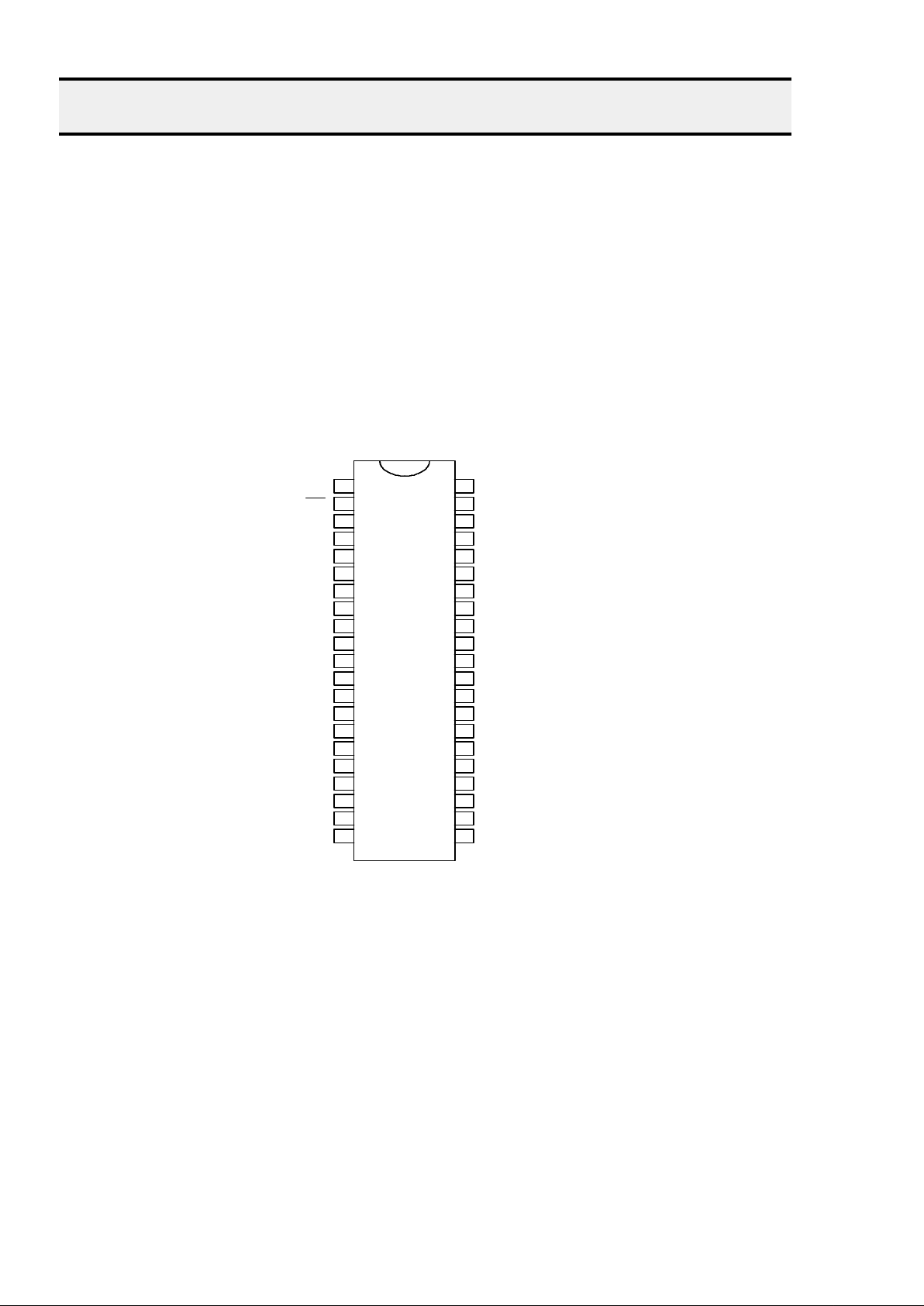
PIN CONFIGURATION
7
36
6 37
20
19
21
18
17
16
15
14
13
12
11
10
9
5
4
3
2
1
PC3 / TOC
42
41
40
39
38
34
33
32
31
30
29
28
27
26
25
24
23
22
Vdisp
P10 / SCK
P11 / SI
P12 / SO
PC2
RESETB
8
XI
XO
VSS / AVSS
TEST
PA0 / AD0
PA1 / AD1
PA2 / AD2
PA3 / AD3
PB0 / AD4
PB1 / AD5
PB2 / AD6
PB3 / AD7
AVDD
VDD
P00 / INT0
P01 / INT1
P02 / INT2 / TI2
P13 / BUZ
P03 / INT3
P20 / CLO
P21
P22
P23
P60
P61
P62
P63
35
P40
P41
P42
P43
P50
P51
P52
P53
D
M
C
4
2
C
3
0
0

2
4Bit Single Chip Microcontroller
DMC42C3008
FEATURES
Memory mapped I/O
PWM
- 14 bit PWM output X 1ch
Program memory : 8192 x 10bits
8-bit serial communication interface
Data memory : 512 x 4bits
- External / Internal clock selection
- Mode : Transmit, Receive
Instructions
Receive only
- Various bit manipulation
Clock continuous
- 8-bit data operation
- 7-bit relative branch
8-bit A/D converter
- 1 byte absolute call
- 8-bit successive approximate type
- 8 channels
Instruction cycle times
- Sample and hold
- Main ( XI = 4.19MHz )
- Conversion time : 17.1us at 4.19MHz
. 15.3 us ( XI/64 = 65.5KHz )
. 1.91 us ( XI/8 = 524.0KHz )
34 I/O Pins
. 0.95 us ( XI/4 = 1.05MHz )
- CMOS Pins : 13
- High voltage Pins : 21
4 Register Bank
- Internal pull-up resistor ( Mask option )
- Internal pull-down resistor ( Mask option )
General register : 8 x 4-bit respectively
Power saving mode
Accumulator
- STOP : Main clock, CPU clock stop
- Bit Accumulator (CY), 4 bit Accumulator (A),
- STBY : Only CPU clock stop
8 bit Accumulator (XA)
Main clock operation
Multiple vectored interrupt source
Operating voltage range
- External interrupt : 4
- VDD = 5V ± 10%
- Internal interrupt : 6
- V
disp
= VDD - 40V
Watch timer(at 4.19MHz)
Package : 42 SDIP
- fast mode : 3.91 msec
- normal mode : 0.5 sec
APPLICATION
- buzzer output : 1, 2, 4 KHz
Microwave Oven, Home Appliances
Basic interval timer
- 8 kinds of period
- Used stabilization wait timer to wake up
Stop mode
One 8-bit timer / event counter
Watchdog timer
- 4 kinds of period
3
4Bit Single Chip Microcontroller
DMC42C3008
P00 ¡- P03
P10 ¡- P13
P20 ¡- P23
P40 ¡- P43
P50 ¡- P53
P60 ¡- P63
PA0 ¡- PA3
PB0 ¡- PB3
PC2 ¡- PC3
TOC / PC3
IRQTC 2
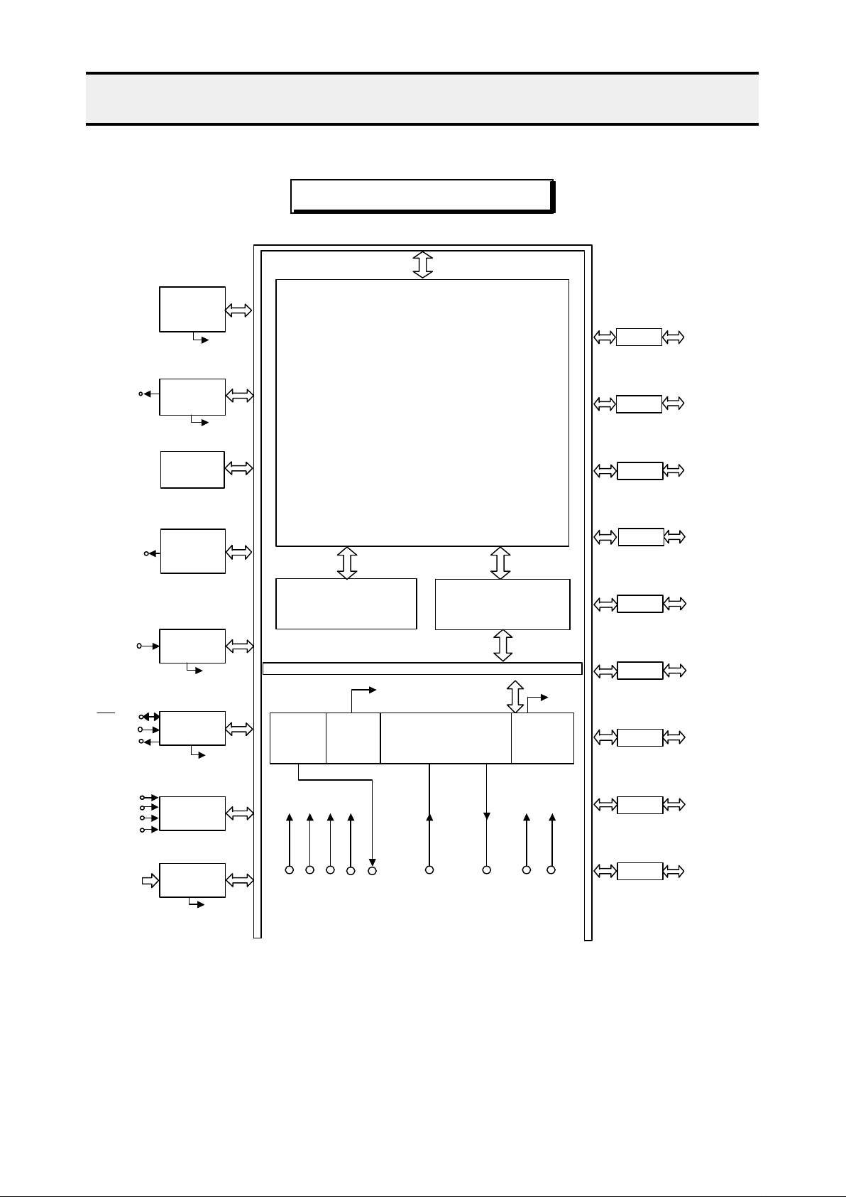
BLOCK DIAGRAM
DMC42CORE
BASIC
INTERVAL
TIMER
IRQBT
WATCH
TIMER
IRQWT
TIMER/EVENT
COUNTER 2
SERIAL
INTERFACE
IRQS0
INTERRUPT
CONTROL
8-BIT ADC
IRQAD
BUZ / P13
TI2 / P02
SCK / P10
SI / P11
SO / P12
INT3 / P03
PA0~PA3,
PB0~PB3/
AD0-AD7
PORT0
PORT1
PORT2
PORT4
PORT5
PORT6
PORTA
PORTB
PORTC
PROGRAM MEMORY
(8192 X 10BITS)
DATA MEMORY
(512 X 4BITS)
Fx / 2
n
CPU
CLOCK
AV
DDAVSSVDD
P20 / CLO
V
SS
XI
XO
RESETB
TEST
CLOCK
OUTPUT
CONTRO
CLOCK
DIVIDER
CLOCK
GENERATOR
STOP/
IDLE
CONTROL
WATCHDOG
TIMER
PULSE WIDTH
MODULATION
INT2 / P02
INT1 / P01
INT0 / P00
4
4Bit Single Chip Microcontroller
DMC42C3008
PROGRAM MEMORY (ROM)
VECTOR ADDRESS
CONTENTS Prioty INTERRUPT SUORCE
0000H
VECTOR
0000H
0 RESET
Reset Signal
ADDRESS AREA
0002H
1 IRQBT
Basic Interval Timer
001FH 0004H
2 IRQ0
External interrupt 0
0020H
ZERO-PAGE
0006H
3 IRQ1
External interrupt 1
CALL AREA
0008H
002FH 000AH
0060H 000CH
6 IRQ2
External interrupt 2
000EH
7 IRQTC2
Timer Event Counter 2
0010H
8 IRQ3
External interrupt 3
0012H
9 IRQS0
Serial I/O 0
0014H
10 IRQAD
8 bit ADC
8K Byte
0016H
0018H
12 IRQWT
Watch Timer
001AH
13 IRQKS
Key Scan
001CH
1FFFH 001EH
15 -
reserved
DATA MEMORY (RAM)
DIRECT
INDIRECT
STACK
GENERAL
m
@HL
@DE @DL
REGISTER
$00
RB=0
RB=1
PAGE0
RB=2
RB=4
(256 Byte)
MP=0
SPS=0
$FF
$00
PAGE1
(256 Byte)
MB=0
MB=0
MP=1
SPS=1
BANK 0
$FF
(1K)
$00
PAGE2
(256 Byte)
MP=2
SPS=2
$FF
$00
PAGE3
I/O
(256 Byte)
MEMORY
MP=3
; Usable
$FF
5
4Bit Single Chip Microcontroller
DMC42C3008
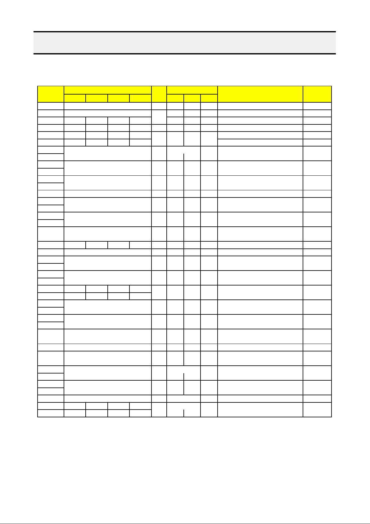
I/O ADDRESS MAP
ADDRESS Hardware Module Name R/W Addressing Unit REMARKS INITIAL
b3 b2 b1 b0 1 bit 4 bit 8bit VALUE
318H Stack pointer low (SPL) R/W O Stack pointer low E
319H Stack pointer high (SPH) R/W O stack pointer high F
31AH SP3 SP2 SP1 SP0 R/W O Stack Page Select Low (SPSL) 0
31BH - - SP5 SP4 R/W O Stack Page Select High (SPSh) 0
31CH AC IS1 IS0 R/W O O O Psw low (PSWL) 0
31DH CY Z OV T Psw high (PSWH) 0
32CH T/E counter mode register 2 W 32CH.3 clock source select. counter 00
32DH (TMOD2) start (ch2)
32EH T/E counter register 2 R readable count value (ch2) 00
32FH (TMCNT2)
330H T/E reference register 2 W count reference register (ch2) FF
331H (TMREF2)
332H Basic Timer mode register(BMOD) R/W 332H.3 clock select, Bit start 0
334H Basic interval timer count R readable count register 00
335H register(BITCNT)
336H Watch timer mode register R/W 336H.3 clock/buzzer select. bit3 00
337H (WMOD) readable
338H Watch dog timer mode register W clock source sel. timer EN/DIS 00
(WDTM)
339H WDTF R WDT flag 0
340H Pwm mode register0(PWMOD0) R/W 6.14bit pwm counter EN/DIS 0
342H Pwm0 data register high W O 14bit pwm data register high 00
343H (PWMODH)
344H Pwm0 data register low W O 14bit pwm data register low 00
345H (PWMODL)
354H PWM3 PWM2 PWM1 PWM0 W O pwm output enable mode 00
355H PWM6 PWM5 PWM4 register (PWM0 = 14bit)
386H Adc8 mode register (ADCM8) R/W 386H.3 O analog input pin select. start & 00
387H low 4bit readable
388H Adc8 output latch (ADCOL8) R O 8bit conversion data 00
389H
3A0H Power control register O system clock select, idle, stop 00
(PCON) R/W mode
3A2H Operating mode register (SCMOD) R/W O main/sub system clock select 0
3A4H Clock output mode register W O cpu clock output select, clock 00
(CLOMD) out EN/DIS
3A8H Serial interface mode register0 W 3A8H.3 O receive/transmit mode. clock 00
3A9H (SIOM0) select
3AAH Serial interface buffer0 R/W serial shift register 0 XX
3ABH (SBUFF0)
3B2H Power on flag (PONF) P/W 3B2H.0 O power on reset flag 0
3C2H IME R/W 3C2H.3 O Interrupt priorty select, IME flag. 00
3C3H IPSR3 IPSR2 IPSR1 IPSR0
6
4Bit Single Chip Microcontroller
DMC42C3008
ADDRESS Hardware Module Name R/W Addressing Unit REMARKS INITIAL
b3 b2 b1 b0 1 bit 4 bit 8bit VALUE
3C4H External interrupt mode register0 W O external interrupt 0 edge 00
(IMOD0) detection
3C5H External interrupt mode register1 W O external interrupt 1 edge 00
(IMOD1) detection
3C6H External interrupt mode register2 W O external interrupt 2 edge 00
(IMOD2) detection
3C7H External interrupt mode register3 W O external interrupt 3 edge 00
(IMOD3) detection
3D8H IE2 IRQ2 IEBT IRQBT R/W O O Interrupt EN/IRQ flag 0
3D9H IEAD8 IRQAD8 IEWT IRQWT R/W O O Interrupt EN/IRQ flag 0
3DAH IES0 IRQS0 R/W O O Interrupt EN/IRQ flag 0
3DBH R/W O O Interrupt EN/IRQ flag 0
3DCH IE1 IRQ1 IE0 IRQ0 R/W O O Interrupt EN/IRQ flag 0
3DDH IETC2 IRQTC2 R/W O O Interrupt EN/IRQ flag 0
3DEH IE3 IRQ3 R/W O O Interrupt EN/IRQ flag 0
3E0H PW03 PW02 PW01 PW00 W O port 0, 1 mode register (PMGA) 00
3E1H PW13 PW12 PW11 PW10
3E2H PW23 PW22 PW21 PW20 W O port 2, 3 mode register (PMGB) 00
3E3H PW33 PW32 PW31 PW30
3E4H PW43 PW42 PW41 PW40 W O port 4, 5 mode register (PMGC) 00
3E5H PW53 PW52 PW51 PW50
3E6H PW63 PW62 PW61 PW60 W O port 6, 7 mode register (PMGD) 00
3E7H PW73 PW72 PW71 PW70
3EAH PWA3 PWA2 PWA1 PWA0 W O port a, b mode register (PMGF) 00
3EBH PWB3 PWB2 PWB1 PWB0
3ECH PWC3 PWC2 PWC1 PWC0 W O port c, d mode register (PMGG) 00
3EDH PWD3 PWD2 PWD1 PWD0
3F0H PORT0 (R0) R/W O O R0 Port Data Register 0
3F1H PORT1 (R1) R/W O O R1 Port Data Register 0
3F2H PORT2 (R2) R/W O O R2 Port Data Register 0
3F4H PORT4 (R4) R/W O O O R4 Port Data Register 0
3F5H PORT5 (R5) R/W O O R5 Port Data Register 0
3F6H PORT6 (R6) R/W O O R6 Port Data Register 0
3FAH PORTA (RA) R/W O O RA Port Data Register 0
3FBH PORTB (RB) R/W O O RB Port Data Register 0
3FCH PORTC (RC) R/W O O O RC Port Data Register 0

7
4Bit Single Chip Microcontroller
DMC42C3008
PIN DESCRIPTION
PIN SHARED I/O FUNCTION RESET PORT
SYMBOL PIN TYPE
P00 INT0
P01 INT1 I/O 4-BIT I/O HIGH VOLTAGE PORT BHPS
P02 INT2/TI2 PORT 0
P03 INT3
P10 SCK
P11 SI I/O 4-BIT I/O PORT BP
P12 SO PORT 1
P13 BUZ ( P13 HIGH VOLTAGE PIN ) BHP
P20 CLO I/O 4-BIT I/O HIGH VOLTAGE PORT BHP
P21~ P23 - PORT 2
P4 - 4-BIT I/O HIGH VOLTAGE PORT. PORT4 BHP
P5 - 4-BIT I/O HIGH VOLTAGE PORT. PORT5 BHP
P6 - 4-BIT I/O HIGH VOLTAGE PORT. PORT6 BHP-PDND
PA AD0~AD3 4-BIT I/O PORT. PORTA BP
PB AD4~AD7 4-BIT I/O PORT. PORTB BP
PC2 - 2-BIT I/O PORT. PORTC BP
PC3 TOC
INT0 P00 External interrupt input port INPUT
INT1 P01 I rising/falling edge detection BHPS
INT2/TI2 P02 Event pulse input port for the
INT3 P03 timer/event counters
SCK P10 I/O Serial clock in/out port
SI P11 I Serial data input port BP
SO P12 O Serial data output port
BUZ P13 O Buzzer output port BHP
CLO P20 O Clock output port BHP
TOC PC3 O PWM output port BP
Key scan P4-P5 I 4, 6, 8 bits Key scan input selectable BHP
AD0~AD3 PA Analog input for the 8-bit A/D converter
AD4~AD7 PB
XI, XO are the input and output, resp-
- ectively, of an inverting amplifier. The pins
can be configured for use as an on-chip
oscillator.
RESETB - I Reset input pin BIN
TEST - I Normally connect to VSS BIN
Vdisp - Used as a high-voltage output power
supply pin.
AVDD, AVSS
- Power & ground for the A/D converter
VDD, VSS - Power & ground
* Note ) P4, P5 : 8-bit operation possible
I
I
O
XI
X
BIN
BOU
BP

8
4Bit Single Chip Microcontroller
DMC42C3008
I/O CIRCUITS
NOTE) PDR : Pull-Down Resistor
PUR : Pull-Up Resistor
M.O : Mask Option
PAD
INTERNAL
BP BHP
BHPSBHP-PDND
OUTPU
DATA
INTERNAL
VDD
VDISP
OUTPUT
ENABLE
DATA
INTERNAL
VDD
VDISP
Output TR
Disable
(P-CH)
PDR
(M.O)
PDR
(M.O)
OUTPU
DATA
VSS
VDD
OUTPU
DATA
INTERNAL
PDR
VDD
PUR
(M.O
VD

9
4Bit Single Chip Microcontroller
DMC42C3008
I/O CIRCUITS
BIN BOUT
PAD
INTERNAL
PAD
INTERNAL

10
4Bit Single Chip Microcontroller
DMC42C3008
ABSOLUTE MAXIMUM RATINGS
(TA = 0¡É to 70¡É, VDD = 5V ±10%, fX = 4.19MHz)
PARAMETER SYMBOL CONDITION RATING UNIT
Supply Voltage VDD -0.3 to + 6.0 V
Programming Voltage VPP Note 1 -0.3 to 13.0 V
Pin Voltage VT Note 2 -0.3 to VDD+0.3 V
Note 3 VDD-45 to VDD+0.3
Total Permissible Input Current
¢²IO
Note 4 70 mA
Total Permissible Output Current
-¢²IO
Note 5 150 mA
Maximum Input Current IO Note 6, 7 4 mA
Note 6, 8 20
Maximum Output Current -IO Note 9, 10 4 mA
Note 10, 11 30
Operating Temperature TA -40 to +85
¡É
Storage Temperature Tstg -55 to +125
¡É
Vdisp Voltage
Vdisp Note 12 VDD - 40 V
Notes : Permanent damage may occur if these absolute maximum rating are exceeded. Normal
operation must be under the conditions stated in the electrical characteristics tables. If these
conditions are exceeded, the LSI may malfunction or its reliability may be affected.
1. Applies to pin AVDD ( VPP ) of DMC42P3008.
2. Applies to all standard voltage pins.
3. Applies to all high voltage pins.
4. The total permissible input current is the total input currents simultaneously flowing in from
all I/O pins to VSS.
5. The total permissible output current is the total output currents simultaneously flowing out
from VDD to all I/O pins.
6. The maximum input current is the maximum current flowing from each I/O pin to VSS.
7. Applies to ports PA, PB.
8. Applies to ports P1, PC.2, PC.3.
9. Applies to ports P1, PA, PB, PC.2, PC.3.
10. The maximum output current is the maximum current flowing from VDD to each I/O pin.
11. Applies to ports P0, P1.3, P2, P4, P5 and P6.
12. The maximum applied voltage is VDD - 40V.

11
4Bit Single Chip Microcontroller
DMC42C3008
DC ELECTRICAL CHARACTERISTICS
PARAMETER SYMBOL TEST
CONDITION
Supply Voltage VDD VDD
High Level VIH RESETB
Input Voltage SCK, SI
INT0~3
TI2
XI
Low Level VIL RESETB
Input Voltage SCK, SI
INT0~3
TI2
XI
High Level VOH SCK, SO
OH = 0.5mA
Output Voltage TOC
Low Level VOL SCK, SO IOL = 0.4mA
Output Voltage TOC
I/O Leakage | IIL |
VIN = 0 V to VDD
Current SCK, SI, SO
XI
INT0~3 VIN = VDD - 40V
TI2 to VDD
Supply Current IDD VDD = 5V
fX = 4MHz
ISBY
DD = 5V
fX = 4MHz
ISTOP VDD = 5V
MAX.
TYP.
MIN.
UNIT
NOT
5.5-4.5-VDD+0.
V
0.8V
DD
V
-
-
VDD-
V
-
0.2VDD-0.3
V
-
0.2V
DD
VDD-40
V
-
0.5
-0.3
V
-
-
VDD-
V
-
0.4
-
V
-
3
-
uA
-
15
-
uA
-
10
-
mA
-
5
-
mA
-
2
-
uA12, 5
3, 5
4
(VSS = 0, VDD = 5V ±10%, TA = 25¡É, fX = 4.19MHz)
LIMIT

12
4Bit Single Chip Microcontroller
DMC42C3008
Notes : 1. Excludes current flowing through pull-up MOS output buffers.
2. I
DD
is the source current when no I/O current is flowing while the MCU is in reset state.
Test condition : MCU : Reset
Pins : RESETB, TEST at VSS
P1.0~1.2, PA, PB, PC.2~3 at V
DD
P0, P1.3, P2, P4, P5, P6 at Vdisp
3. ISBY is the source current when no I/O current is flowing while the MCU timer is operating.
Test condition : MCU : I/O Reset
Standby mode
Pins : RESETB at VDD
TEST at VSS
P1.0~1.2, PA, PB, PC.2~3 at VDD
P0, P1.3, P2, P4, P5, P6 at Vdisp
4. This is the source current when no I/O current is flowing.
Test condition : Pins : P1.0~1.2, PA, PB, PC.2~3 at VDD
P0, P1.3, P2, P4, P5, P6 at VSS
XI clock stop after stop mode
5. Current dissipation is in proportion to fX while the MCU is operating or in standby mode.

13
4Bit Single Chip Microcontroller
DMC42C3008
DC ELECTRICAL CHARACTERISTICS
1. STANDARD I/O PINS
PARAMETER SYMBOL TEST LIMIT UNIT NOTE
CONDITION MIN. TYP. MAX.
High Level VIH P10~2,PC2~3 0.8VDD - VDD+0.3 V
Input Voltage PA,PB
Low Level VIL P10~2,PC2~3 -0.3 - 0.3VDD V
Input Voltage PA,PB
High Level VOH P10~2,PC2~3 -IOH = 0.5mA VDD-0.5 - - V
Output Voltage PA,PB
Low Level VOL P10~2,PC2~3 IOL = 1.6mA - - 0.4 V
Output Voltage PA,PB
Input Leakage
| IOL | P10~2,PC2~3 VIN = 0V to VDD - - 3 uA 1
Current PA, PB
Note : 1. Output buffer current is excluded.
2. HIGH VOLTAGE I/O PINS
PARAMETER SYMBOL TEST LIMIT UNIT NOTE
CONDITION MIN. TYP. MAX.
High Level VIH P0,P13,P2 0.8VDD - VDD+0.3 V
Input Voltage P4, P5, P6
Low Level VIL P0,P13,P2 VDD-40 - 0.3VDD V
Input Voltage P4, P5, P6
High Level VOH P0,P13 -IOH = 15mA VDD-3.0 - - V
Output Voltage P2, P4, P5 -IOH = 10mA VDD-2.0 - - V
P6, BUZ -IOH = 4mA VDD-1.0 - - V
Low Level VOL P0,P13
disp = VDD
- 40V
- - VDD-37 V 1
Output Voltage P2, P4, P5
150§Ú at
- - VDD-37 V 2
P6, BUZ VDD - 40 V
Input Leakage
| IOL | P0,P13
disp = VDD
- 40V
- - 20 uA 3
Current P2, P4, P5 to VDD
P6, BUZ
Pull-down Id P0,P13,P2 Vdisp = VDD
- 35V
200 - 1000 uA 1
MOS Current
P4,P5,P6,BUZ
VIN = VDD
Notes : 1. Applies to pins with pull-down MOS as selected by the mask option.
2. Applies to pins without pull-down MOS as selected by the mask option.
3. Excludes outputs buffer current.
VDD = 4.5 to 5.5V, VSS = 0V, Vdisp = VDD - 40V to VDD
(VSS = 0, VDD = 5V ±10%, TA = 25¡É, fX = 4.19MHz)

14
4Bit Single Chip Microcontroller
DMC42C3008
AC ELECTRICAL CHARACTERISTICS
(TA = -40 to +85¡É, VDD = 2.7 to 6.0V)
PARAMETER SYMBOL TEST CONDITION MIN. TYP. MAX. UNIT
Cycle Time 0.95 - 64 uS
3.8 - 64 uS
TI Input Frequency 0 - 1 MHz
TI Input High, Low 0.48 - - uS
Level Width
SCK Cycle Time Input 800 - - nS
Output 950 - - nS
SCK High, Low Level Width Input 400 - - nS
Output - - nS
SI Set up Time to SCK High 100 - - nS
SI Hold Time to SCK High 400 - - nS
SCK to S0 Output Input - - 300 nS
Delay Time Output - - 250 nS
INT 0 ~ 4 Input Level
5 - - uS
High, Low 5 - - uS
RESETB Low Level 5 - - uS
VDD = 4.5 to 6.0V
VDD = 2.7 to 3.3V
VDD = 4.5 to 6.0V
VDD = 4.5 to 6.0V
t
CY
f
TI
t
TIH
t
KCY
VDD = 4.5 to
VDD = 4.5 to
t
KH
t
KSI
t
SIK
t
KSO
VDD = 4.5 to
t
RSL
t
KCY
/2~50
t
INTHtINTL

15
4Bit Single Chip Microcontroller
DMC42C3008
AC Timing Measurement Points (Except XI and XTI)
Measurement
0.8VD0.2VD0.8V
D
1/XI
1/XTI
1/fTI
tKC
tINT tINT
tXL
tXH
tXTL
tXT
tTIL tTIH
tKL tKH
tRS
tSIK tKSI
0.2V
D
Input Data
Output Data
VDD-
0.4V
VDD-
0.4V
0.8V
D
0.2V
D
0.8V
D
0.2V
D
0.8V
D
0.2V
D
0.2V
D
Clock Timing
XI
XTI
TI0
Serial Transfer Timing
SCK
SI
SO
Interrupt Input Timing
INT0~3
KS0~7
RESET
RESETB Input Timing
Timer Event Counter

16
4Bit Single Chip Microcontroller
DMC42C3008
RAM DATA RETENTION CHARACTERISTICS ( in STOP Mode )
(TA = -40 to +85¡É)
PARAMETER SYMBOL TEST CONDITION MIN. TYP. MAX. UNIT
2.0 - 6.0 V
- 0.1 10 uA
0 - - uS
When released by RESETB -
217/fx
- mS
- NOTE 1) - mS
NOTE 1) Depends on the setting of the basic interval timer mode register.
(refer to the table below)
( fX = 4.19MHz )
BMOD2 BMOD1 BMOD0 Oscillation Stabilization
0 0 0
220/fX (Approximately 250ms)
0 1 1
217/fX (Approximately 31.3ms)
1 0 0
215/fX (Approximately 7.82ms)
1 0 1
213/fX (Approximately 1.95ms)
Data Retention
Supply Voltage
Data Retention
Supply Current
Release Signal Set
Time
VDDDR
IDDDR
tSREL
VDDDR = 2.0V
When released by interrupt
Signal
Oscillation
Stabilization
tWAIT

17
4Bit Single Chip Microcontroller
DMC42C3008
RAM DATA RETENTION TIMING
When STOP mode is released by RESETB input
When STOP mode is released by interrupt signal
STOP Mode
RAM Data retention
VDDDR
VDD
tSREL
t
WAI
STOP instruction execution
Operation
Stabilization Wait Time
STOP Mode
RAM Data retention
VDDDR
VDD
t
WAI
STOP instruction execution
RESET
Interrupt Signal
(Rising Edge)
Internal Reset Operation
Stabilization Wait Time
Operation

18
4Bit Single Chip Microcontroller
DMC42P3008
DESCRIPTION
The DMC42P3008 is a system evaluation LSI having a built in One-time PROM for DMC42C3008.
A programming and verification for the internal PROM is achieved by using a general EPROM
programmer with an adapter socket. The function of this device is exactly same as the
DMC42C3008 by programming to the internal PROM. The DMC42P3008 is OTP version
of the DMC42C3008 whose internal ROM has been changed from MASK ROM to EPROM.
* CAUTION : P3008 does not include internal pull-down resistor for high voltage output,
so user has to connect externally.
PIN CONFIGURATION
RESETB
XO
VSS / AVSS
PA1 / AD1
PA0 /
TEST
PA2 / AD2
PB0 / AD4
PA3 / AD3
VDD
VPP / OEX / AVDD
PC2
P20 / CLO
P02 / INT2 / TI2
P13 / BUZ
P01 /
P00 / INT0
1
7
3
6
4
5
8
12
XI
Vdisp
21
PB1 / AD5
PB2 / AD6
PB3 / AD7
P10 / SCK
P11 / SI
PC3
P12 / SO
10
9
11
13
15
14
20
35
17
19
18
16
2
42
36
40
37
39
38
33
34
35
31
30
28
29
P53
P52
P41
P51
P42
P50
P43
P61
P62
P63
P60
P23 /
P21
P22
P40
26
24
25
23
22
27
32
41
EPA13
EPA12
CEX
EPA8
EPA0
EPD3
EPD0
EPD2
EPD1
EPA11
D
M
C
4
2
P
3
0
0
EPA9
EPA10
EPD4
EPA1
EPA
EPA
EPA4
EPA5
EPA6
EPA7
P03 / INT3
DMC42P3008

19
4Bit Single Chip Microcontroller
DMC42P3008
DEVICE OPERATION
The operational modes of the DMC42P3008 are listed in Table 1.
A single 5V power supply is required in the read mode.
All inputs are TTL levels except for VPP / OEX.
PINS
MODE
READ 5.0V
PROGRAM 6.0V
VERIFY 6.0V
PROGRAM INHIBIT 6.0V High Z
TABLE 1. Operating Modes
MODE
EPROM MODE USER MODE
TEST
TABLE 2. The modes of DMC42P3008
DC PROGRAMMING CHARACTERISTICS
LIMIT UNIT
MIN. MAX.
Input Low Voltage -0.1 0.8 V
Input High Voltage 2.0 V
Output Low Voltage during Verify - 0.45 V
Output High Voltage during Verify 2.4 - V
Quick-pulse Programming 12.5 13.0 V
Quick-pulse Programming 6.0 6.5 V
CEX VPP / OEX
VDD
OUTPU
PIN NAME
RESETB
V
IL
VDDVILVIHVOLVOHVPPVDDIOL = 2.1mA
VILVILVILVILVPPVILVPPVIHDIND
OUT
D
OUT
VIHV
IL
V
PP
= 12.5±0.5V
TEST CONDITIONPARAMETER
SYMBO
IOH = -400uA

20
4Bit Single Chip Microcontroller
DMC42C/P3008
PACKAGE DIMENSION
[ UNIT : Millimeter ]
14.6Max
42
1 21
22
14.0
15.24
0°~ 15°
0.25
+0.11
-0.05
37.34
38.6Max
1.778±0.250
0.48±0.10
1.0
5.08Max
2.54Mi
0.51Mi
42 SDIP
 Loading...