

Page 1

FILE NO. SM-CTV-O-056
COLOR TELEVISION
SERVICE MANUAL
MODEL NO.
PF2720/PF2730
PF3220/PF3230
CHASSIS NO. CH-16CD
Please read this manual carefully before service.
Page 2

SERVICE MANUAL
TABLE OF CONTENTS
SAFETY INSTRUCTIONS AND MAINTENANCE
X-Ray Radiation Precaution ..............................................................................................1
Safety Precaution................................................................................................................1
Product Safety Notice.........................................................................................................2
Maintenance ......................................................................................................... 3
SPECIFICATIONS..........................................................................................................4
KEY ICS AND ASSEMBLIES.................................................................................4
.....................................1
SYSTEM BLOCK DIAGRAMS
Structure Block Diagram....................................................................................................5
Block Diagram for Supply Voltage System.....................................................................6
...............................................................................5
SERVICE DATA...............................................................................................................7
Technical Data of Key ICs..................................................................................................7
Service Data of Key ICs.....................................................................................................22
Waveforms of Key Points...................................................................................................29
ADJUSTMENTS..............................................................................................................37
Set-up Adjustments.............................................................................................................37
Circuit Adjustments.............................................................................................................40
Service Mode and Bus Data..............................................................................................41
TROUBLESHOOTING FLOW CHARTS.........................................................47
APPENDIX
1. Circuit Diagrams
2. Printed Circuit Board Diagrams
3. Final Wiring Diagrams
4. Exploded Views
2
Page 3

SAFETY INSTRUCTIONS AND MAINTENANCE
WARNING: BEFORE SERVICING THIS CHASSIS, READ THE “X-RAY RADIATION
PRECAUTION”, “SAFETY PRECAUTION”AND “PRODUCT SAFETY NOTICE
INSTRUCTIONS BELOW.
”
X-RAY RADIATION PRECAUTION
1. The EHT must be checked every time the TV is serviced to ensure that the CRT does not emit
X-ray radiation as result of excessive EHT voltage. The maximum EHT voltage permissible in
any operating circumstances must not exceed the rated value. When checking the EHT, use
the High Voltage Check procedure in this manual using an accurate EHT voltmeter.
2. The only source of X-RAY radiation in this TV is the CRT. The TV minimizes X-RAY radiation,
which ensures safety during normal operation. To prevent X-ray radiation, the replacement
CRT must be identical to the original fitted as specified in the parts list.
3. Some components used in this TV have safety related characteristics preventing the CRT from
emitting X-ray radiation. For continued safety, replacement component should be made after
referring the PRODUCT SAFETY NOTICE below.
4. Service and adjustment of the TV may result in changes in the nominal EHT voltage of the
CRT anode. So ensure that the maximum EHT voltage does not exceed the rated value after
service and adjustment.
SAFETY PRECAUTION
WARNING: REFER SERVICING TO QUALIFIED SERVICE PERSONNEL ONLY.
1. The TV has a nominal working EHT voltage. Extreme caution should be exercised when
working on the TV with the back removed.
1.1 Do not attempt to service this TV if you are not conversant with the precautions and
procedures for working on high voltage equipment.
1.2 When handling or working on the CRT, always discharge the anode to the TV chassis before
removing the anode cap in case of electric shock.
1.3 The CRT, if broken, will violently expel glass fragments. Use shatterproof goggles and take
extreme care while handling.
1.4 Do not hold the CRT by the neck as this is a very dangerous practice.
2. It is essential that to maintain the safety of the customer all power cord forms be replaced
exactly as supplied from factory.
3. Voltage exists between the hot and cold gro und when the TV is in operation. Install a suitable
isolating transformer of beyond rated overall power when servicing or connecting any test
equipment for the sake of safety.
1
Page 4

SERVICE MANUAL
4. When replacing ICs, use specific tools or a static-proof electric iron with small power (below
35W).
5. Do not use a magnetized screwdriver when tightening or loosing the deflection yoke assembly
to avoid electronic gun magnetized and decrement in convergence of the CRT.
6. When remounting the TV chassis, ensure that all guard devices, such as nonmetal control
buttons, switch, insulating sleeve, shielding cover, isolating resistors and capacitors, are
installed on the original place.
7. Replace blown fuses within the TV with the fuse specified in the parts list.
8. When replacing wires or components to terminals or tags, wind the leads around the terminal
before soldering. When replacing safety components identified by the international hazard
symbols on the circuit diagram and parts list, it must be the company-approved type and must
be mounted as the original.
9. Keep wires away from high temperature components.
PRODUCT SAFETY NOTICE
CAUTION: FOR YOUR PROTECTION, THE FOLLOWING PRODUCT SAFETY NOTICE
SHOULD BE READ CAREFULLY BEFORE OPERATING AND SER VICING THIS TV SET.
1. Do not slap or beat the cabinet or CRT, since this may result in fire or explosion.
2. Never allow the TV sharing a plug or socket with other large-power equipment. Doing so may
result in too large load, thus causing fire.
3. Do not allow anything to rest on or roll over the power cord. Protect the power cord from being
walked on, modified, cut or pinched, particularly at plugs.
4. Do not place any objects, especially heavy objects and lightings, on top of the TV set. Do not
install the TV near any heat sources such as radiators, heat registers, stove, or other
apparatus that produce heat.
5. Service personnel should observe the SAFETY INSTRUCTIONS in this manual during use
and servicing of this TV set. Otherwise, the resulted damage is not protected by the
manufacturer.
6. Many electrical and mechanical components in this chassis have special safety-related
characteristics. These characteristics are often passed unnoticed by a visual inspection and
the X-ray radiation protection afforded by them cannot necessarily be obtained by using
replacements rated at higher voltages or wattage, etc. Components which have these special
safety characteristics in this manual and its supplements are identified by the international
hazard symbols on the circuit diagram and parts list. Before replacing any of these
components read the parts list in this manual carefully. Substitute replacement components
which do not have the same safety characteristics as specified in the parts list may create
X-ray radiation.
2
Page 5

SERVICE MANUAL
Safety Symbol Description
The lightning symbol in the triangle tells you that the voltage inside this product may
be strong enough to cause an electric shock. Extreme caution should be exercised
when working on the TV with the back removed.
This is an international hazard symbol, telling you that the components identified by
the symbol have special safety-related characteristics.
FDA This symbol tells you that the critical components identified by the FDA marking have
special safety-related characteristics.
UL This symbol tells you that the critical components identified by the UL marking have
special safety-related characteristics.
MAINTENANCE
1. Install the TV set on a stable and level surface. Do not place the set near or over a radiator or
heat register, or where it is exposed to direct sunlight.
2. Do not install the TV set in a place exposed to rain, water, excessive dust, mechanical
vibrations or impacts.
3. Allow enough space (at least 10cm) between the TV and wall or enclosures for proper
ventilation.
4. Slots and openings in the cabinet should never be blocked by clothes or other objects.
5. Please power off the TV set and disconnect it from the wall immediately if any abnormal
condition are met, such as bad smell, belching smoke, sparkling, abnormal sound or no
picture/sound/raster. Hold the plug firmly when disconnecting the power cord.
6. Unplug the TV set from the wall outlet before cleaning or polishing it. Use a dry soft cloth for
cleaning the exterior of the TV set or CRT screen. Do not use liquid cleaners or aerosol
cleaners.
3
Page 6
SERVICE MANUAL
SPECIFICATIONS
MODEL PF2720 PF2730 PF3220 PF3230
Television System NTSC-M
Channel Coverage VHF 2-13, UHF 14~69
Cable TV Coverage
Channels Preset 181
Antenna Input 75 ohm (unbalanced)
Screen Dimensions
Audio Output 5W+5W 5W+5W
Power Source ~120Vac 60Hz
Unit Weight 97.9lbs. ( 44.5kg) 156lbs. ( 71kg)
Unit Dimensions
Packaged
Dimensions
Power
Consumption
Hyper Band (AA~ZZ, AAA, BBB)/Ultra Band (65~94, 100~125)
21.26x 15.94 in
29.09x22.83x19.29 in.
739x580x490mm
33.07x26.38x23.43in.
840x670x595mm
Mid Band (A-8~A-1, A~I)/Super Band (J~W)
25.20x 18.82 in
540x405 mm
135W 170W
640x478 mm
33.70x26.34x22.05 in.
856x669x560mm
40x30.55x27.76in.
1016x776x705mm
KEY ICS AND ASSEMBLIES
Table 1 Key ICs and Assemblies
Serial No. Position No. Model No. Function Description
1 N201 TDA937X UOC
2 N202 AT24C16 EEPROM
3 NB01 MSP3440G-B8 BTSC
4 N401 TDA8350 Vertical output circuit
5 N361 TDA8944J Sound power amplifier
6 N901 TA1219AN
7 N902 TC90A49P
8 NY01 TDQ6108JF
9 A101 TDQ-6F2-M
10 IC801 STR-G8626
TV/AV switch circuit
COMB filter
Video amplifier
Tuner
Power supply circuit
4
Page 7

SYSTEM BLOCK DIAGRAMS
Structure Block Diagram
SERVICE MANUAL
45V
V
5
Page 8

SERVICE MANUAL
Block Diagram for Supply Voltage System
6
Page 9

SERVICE MANUAL
SERVICE DATA
Technical Data of Key ICs
TDA937X (N201)
UOC
1. General Description
The various versions of the TDA937X PS/N2
series combine the functions of a video
processor together with a μ-Controller and
US Closed Caption decoder. The ICs are
intended to be used in economy television
receivers with 90° and 110° picture tubes.
The ICs have supply voltages of 8V and 3.3V
and they are mounted in an S-DIP 64
envelope.
The features are given in the following feature
list. The differences between the various ICs
are given in the table on page 4.
2. Features
TV-signal processor
• Multi-standard vision IF circuit with
alignment-free PLL demodulator
• Internal (switchable) time-constant for the
IF-AGC circuit
• A choice can be made between versions with
mono intercarrier sound FM demodulator and
versions with QSS IF amplifier.
• The mono intercarrier sound versions have a
selective FM-PLL demodulator which can be
switched to the different FM sound
frequencies (4.5/5.5/6.0/6.5 MHz).
The quality of this system is such that the
external band-pass filters can be omitted.
• Source selection between ‘internal’ CVBS and
external CVBS or Y/C signals
• Integrated chrominance trap circuit
• Integrated luminance delay line with
adjustable delay time
• Picture improvement features with peaking
(with variable positive/negative overshoot
ratio), black stretching and Dynamic Skin
Tone Control
• Integrated chroma band-pass filter with
switchable centre frequency
• Only one reference (12 MHz) crystal
required for the μ-Controller, Teletext- and
the colour decoder
• PAL/NTSC colour decoder with automatic
search system
• Internal base-band delay line
• RGB control circuit with ‘Continuous Cathode
Calibration’, white point and black level offset
adjustment so that the colour temperature of
the dark and the light parts of the screen can
be chosen independently.
• Linear RGB or YUV input with fast blanking
for external RGB/YUV sources. The
Text/OSD signals are internally supplied from
theμ-Controller/Teletext decoder
• Contrast reduction possibility during
mixed-mode of OSD and Text signals
• Horizontal synchronization with two control
loops and alignment-free horizontal oscillator
• Vertical count-down circuit
• Vertical driver optimized for DC-coupled
vertical output stages
• Horizontal and vertical geometry processing
• Horizontal and vertical zoom function for 16 :
9 applications
• Horizontal parallelogram and bow correction
for large screen picture tubes
• Low-power start-up of the horizontal drive
circuit
7
Page 10

3.Pin
SERVICE MANUAL
8
Page 11

4.Block Diagram
SERVICE MANUAL
9
Page 12

SERVICE MANUAL
5.Refer to Table 2 about Functions and Service Data of the IC's Each Pin.
10
Page 13
SERVICE MANUAL
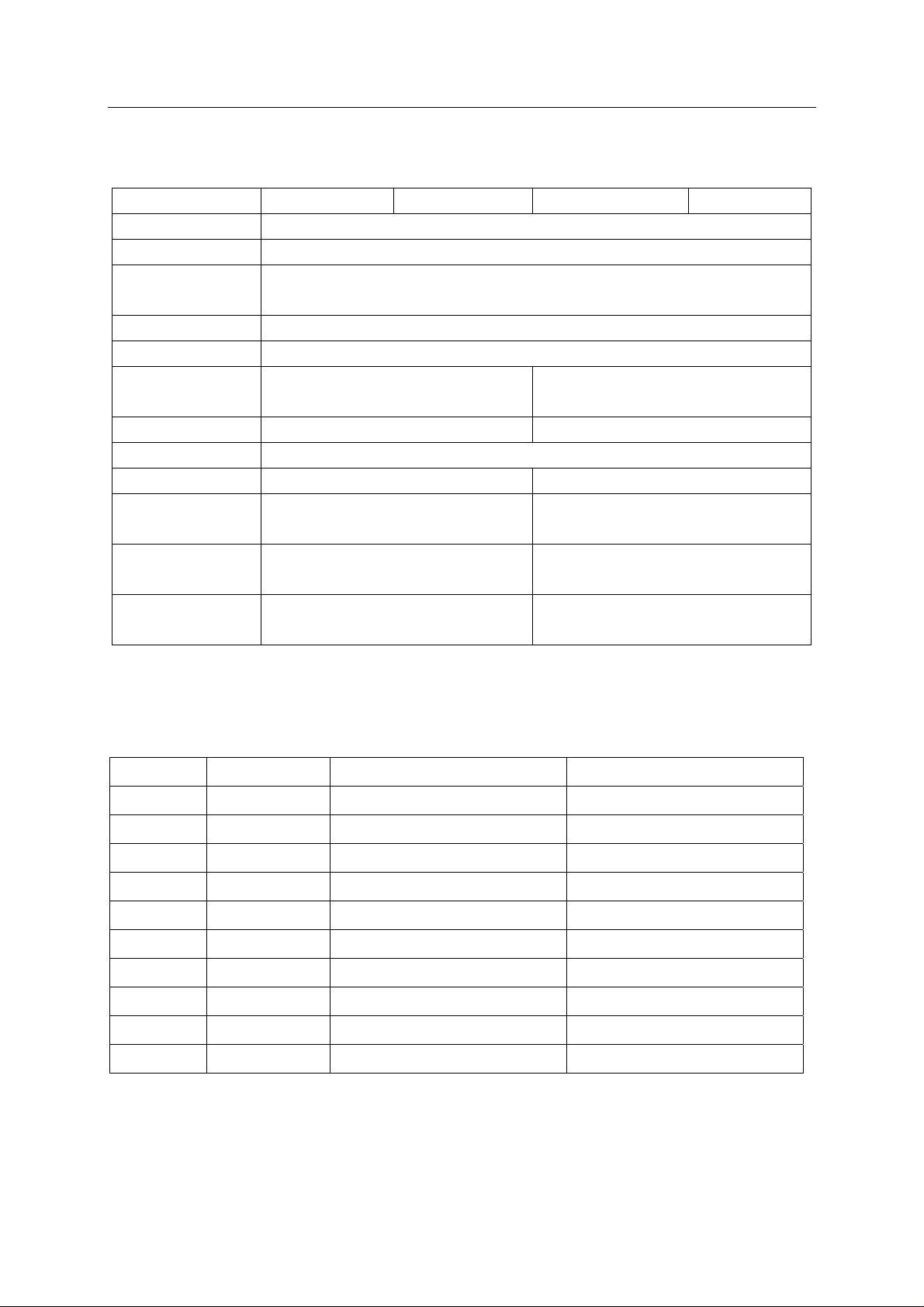
AT24C16 (N202)
EEPROM
1. Features
·Low Voltage and Standard Voltage Operation
5.0 (V
2.7 (V
2.5 (V
1.8 (V
= 4.5V to 5.5V)
CC
= 2.7V to 5.5V)
CC
= 2.5V to 5.5V)
CC
= 1.8V to 5.5V)
CC
·Internally Organized 128 x 8 (1K), 256 x 8 (2K),
512 x 8 (4K),1024 x 8 (8K) or 2048 x 8 (16K)
·2-Wire Serial Interface
·Bidirectional Data Transfer Protocol
·100 kHz (1.8V, 2.5V, 2.7V) and 400 kHz (5V)
Compatibility
·Write Protect Pin for Hardware Data Protection
·8-Byte Page (1K, 2K), 16-Byte Page (4K, 8K,
16K) Write Modes
·Partial Page Writes Are Allowed
·Self-Timed Write Cycle (10 ms max)
·High Reliability
Endurance: 1 Million Cycles
Data Retention: 100 Years
·Automotive Grade and Extended Temperature
Devices Available
·8-Pin and 14-Pin JEDEC SOIC and 8-Pin PDIP
Packages
2.Description
The AT24C01A/02/04/08/16 provides
1024/2048/4096/8192/16384 bits of serial
electrically erasable and programmable read
only memory (EEPROM) organized as
128/256/512/1024/2048 words of 8 bits each.
The device is optimized for use in many
industrial and commercial applications where low
power and low voltage operation are essential.
The AT24C01A/02/04/08/16 is available in space
saving 8-pin PDIP, 8-pin and 14-pin SOIC
packages and is accessed via a 2-wire serial
interface. In addition, the entire family is
available in 5.0V (4.5V to 5.5V), 2.7V (2.7V to
5.5V), 2.5V (2.5V to 5.5V) and 1.8V (1.8V to
5.5V) versions.
Pin Configurations
11
Page 14
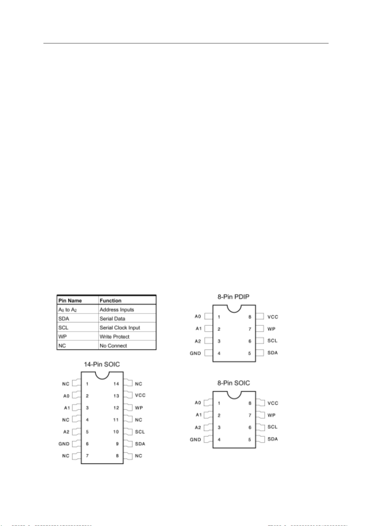
3.Block Diagram
SERVICE MANUAL
Fig.6
4.Refer to Table 3 about Functions and Data of the IC’ s Pins.
12
Page 15
SERVICE MANUAL
MSP3440G-B8 (NB01)
Multistandard Sound Processor Family
Release Note: Revision bars indicate significant
changes to the previous edition. The hardware
and software description in this document is
valid for the MSP34X0G version B5 and
following versions.
1. Introduction
The MSP34X0G family of single-chip
Multistandard Sound Processors covers
the sound processing of all analog
TV-Standards worldwide, as well as the
NICAM digital sound standards. The full TV
sound processing, starting with analog sound
IF signal-in, down to processed analog AF-out,
is performed on a single chip. Figure 7 shows
a simplified functional block diagram of the
MSP34X0G.
This new generation of TV sound processing
ICs now includes versions for processing the
multichannel television sound (MTS) signal
conforming to the standard recommended by
the Broadcast Television Systems Committee
(BTSC). The DBX noise reduction, or
alternatively MICRONAS Noise Reduction
(MNR) is performed alignment free
2. Block Diagram
Other processed standards are the Japanese
FM-FM multiplex standard (EIA-J) and the FM
Stereo Radio standard.
Current ICs have to perform adjustment
procedures in order to achieve good stereo
separation for BTSC and EIA-J.
The MSP34X0G has optimum stereo
performance without any adjustments.
All MSP34X0G versions are pin and
software downward-compatible to the
MSP34X0D. The MSP34X0G further simplifies
controlling software. S tandard selection
requires a single I
The MSP34X0G has built-in automatic
Functions: The IC is able to detect the actual
sound standard automatically (Automatic
Standard Detection). Furthermore, pilot levels
and identification signals can be evaluated
internally with subsequent switching between
mono/stereo/bilingual; no I
necessary (Automatic Sound Selection).
The ICs are produced in submicron CMOS
technology.
The MSP34X0G is available in the following
packages: PLCC68, PSDIP64, PSDIP52, PQFP80
and PLQFP64.
2
C transmission only.
2
C interaction is
Fig. 7 Simplified Functional Block Diagram of the MSP34X0G
3. Refer to Table 4 about Functions and Service Data of MSP34X0G’s Each Pins.
13
Page 16
SERVICE MANUAL
I
(
set
)
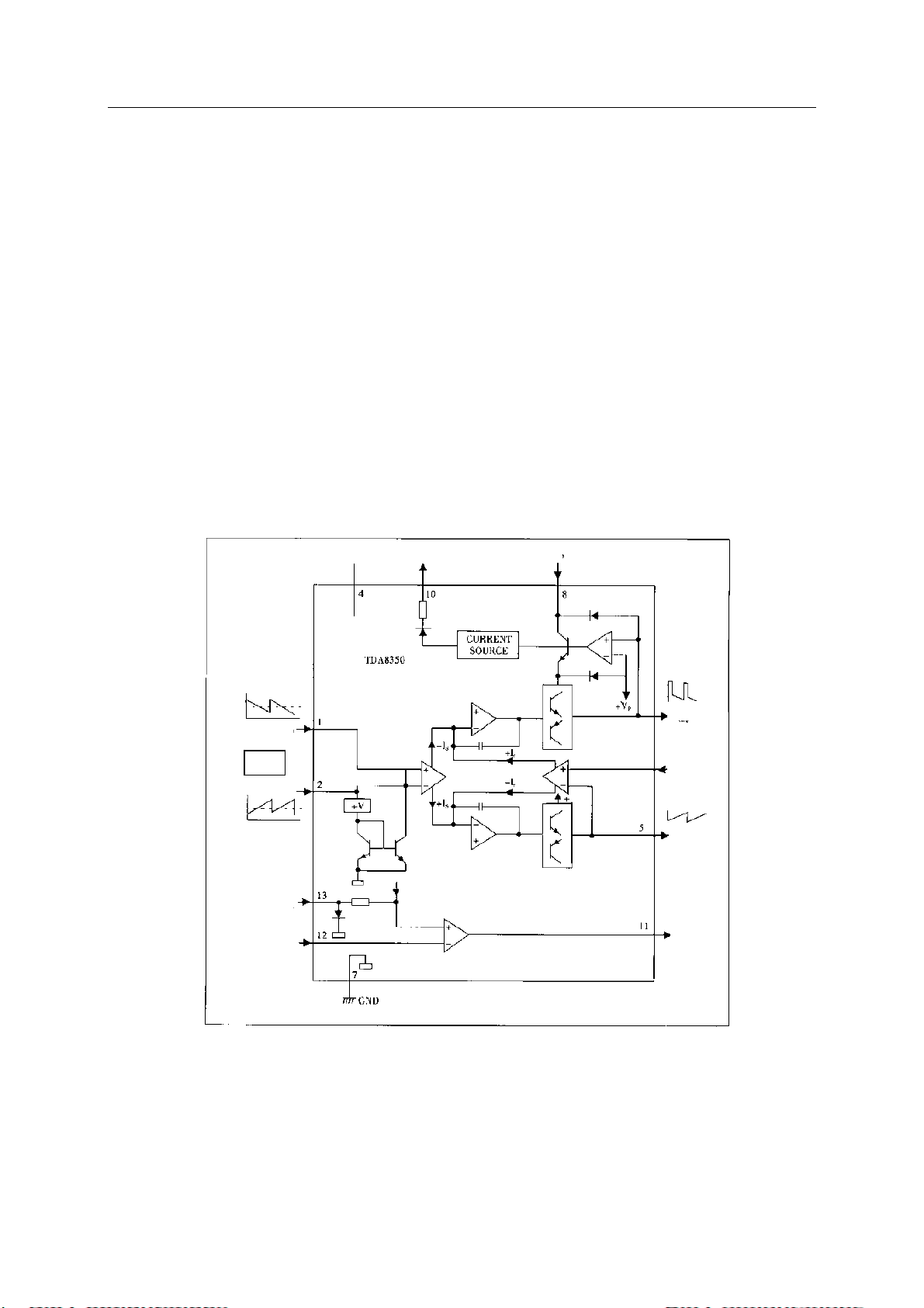
TDA8350 (N401)
DC-coupled Vertical Deflection and East-West Output Circuit
1. Features
·Few external components
·Highly efficient fully DC-coupled vertical output
bridge circuit
·Vertical fl yback switch
·Guard circuit
·Protection against:
-short-circuit of the output pins
-short-circuit of the output pins to Vp
3. Block Diagram
V
V
+V
·High EMC immunity due to common mode
inputs
·Temperature (thermal) protection
·East-West output stage with one single
conversion resistor.
2. General Description
The TDA8350Q is a power circuit for use
in 90° and 110° colour deflection systems
for field frequencies of 50 to 120 Hz. The
circuit provides a DC driven vertical
deflection output circuit, operating as a
highly efficient class G system and an
East-West driver for sinking the diode
modulator current.
V
I
I
+V
I
VP
-V
I
I
I
Fig. 8
4. Refer to Table 5 about Functions and Service Data of TDA8350Q’s Pins.
V
V
V
V
14
Page 17

TDA8944J (N361)
Audio Power Amplifier
SERVICE MANUAL
1. General Description
The TDA8944J is a dual-channel audio power
amplifier with an output power of
2 ´ 7 W at a n 8 W load and a 12 V supply. The
circuit contains two Bridge Tied Load
(BTL) amplifiers with an all-NPN output stage and
standby/mute logic. The TDA8944J
comes in a 17-pin DIL-bent-SIL (DBS) power
package. The TDA8944J is
printed-circuit board (PCB) compatible with all
other types in the TDA894x family.
One PCB footprint accommodates both the mono
and the stereo products.
3.Block Diagram
2. Features
Few external components
Fixed gain
Standby and mute mode
No on/off switching plops
Low standby current
High supply voltage ripple rejection
Outputs short-circuit protected to ground,
supply and across the load
Thermally protected
Printed-circuit board compatible
Pinning
Fig.10 Pin configuration.
5. Refer to Table 6 about Functions and Service Data of TDA8944J's Pins.
15
Page 18
SERVICE MANUAL
TA1219AN (N901)
Audio/Video Switching IC for TVs
The TA1219AN is an audio/video switching IC for TV Sets.
Conforming to I2C bus standards, it allows you to
perform various switching operations through the bus
lines by using a microcomputer. Furthermore, since the
presence of a signal on its sync signal output pin can be
determined by a microcomputer , it is possible to check
each input/output channel (self-diagnosis).
This IC has the same pin assignments as the TA1218AN
(SDIP42), a 2-channel output version of the TA1219AN, so
these chips are pin compatible on pins 3 to 20 and 23 to
40 in TA1218AN.
1. Features
2
·I
C bus control
·Video: 5-channel inputs and 1-channel outputs (2 channels conforming to S system)
·Audio: 5-channel inputs and 2-channel outputs
·Self-diagnostic function
·ADC inputs based on European 21-pin standards
·ADC inputs based on S1/S2 terminal standards
·Switchable subaddress
16
Page 19
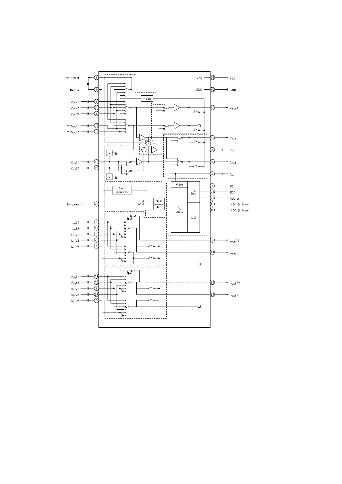
2. Block Diagram
SERVICE MANUAL
Fig.11
3. Refer to Table 7 about Functions and Service Data of TA1219AN’s Pins.
17
Page 20

SERVICE MANUAL
3. Pin Assignment
2. Block Diagram
Fig.14
4. Refer to Table 8 about Fu nctions and Service Data of TC90A49P’s Pins.
TC90A49P (N902)
COMB Filter
1. Features
TV format : NTSC (3.58), PAL, M-PAL, and N-
PAL
Dynamic comb filter
Vertical edge enhancement circuit
PLL 8 × multiplier circuit
Internal 8-bit 4 fsc AD converter
Internal 8-bit precision 8 fsc DA converter (2 ch)
Sync tip clamp circuit
Internal 4H-line memory
2
I C bus interface
Package : DIP 20-pin and SOP 24-pin
5 V single power supply
18
Page 21

TDA6108JF (NY01)
Triple Video Output Amplifier
SERVICE MANUAL
1. Features
·Typical bandwid th of 9.0 MHz for an output
signal of 60 V (peak-to-peak value)
·High slew rate of 1850 V/µS
·No external components required
·Very simple application
·Single supply voltage of 200 V
·Internal reference voltage of 2.5 V
·Fixed gain of 51
·Black-Current Stabilization (BCS) circuit
·Thermal protection.
3. Ordering Information
Number
TDA6108JF DBS9MPF
Name Description Version
Plastic DIL-bent-SIL medium power package with
fin; 9 leads
2. General Description
The TDA6108JF includes three video
output amplifiers in one plastic
DIL-bent-SIL 9-pin medium power
(DBS9MPF)package (SOT 111-1), using
high-voltage DMOS technology, and is
intended to drive the three cathodes of a
colour CRT directly. To obtain maximum
performance, the amplifier should be used
with black-current control.
Package Type
SOT111-1
4. Block Diagram
Fig.15
5. Refer to Table 8 about Functions and Service Data of TDA6108JF’s Pins
.
19
Page 22

SERVICE MANUAL
STR-G8626 (IC801)
The Series STR-G 86626/5653/F6654 is specifically designed to satisfy the requirements for increased
integration and reliability in off-line quasi-resonant flyback converters. The series incorporates a
high-precise error amplifying control and drive circuit with discrete avalanche-rated power MOSFET,
featuring fewer external components, small-size and standard power supply.
Covering the power range from below 25 watts up to 300 watts for 100/115/230 VAC inputs, and up to
150 watts for 85 to 265 VAC universal input, these devices can be used in a range of applications,
from battery chargers and set top boxes, to televisions, monitors, and industrial power supply units.
Cycle-by-cycle current limiting, under-voltage lockout with hysteresis, over-voltage protection, and
thermal shutdown protects the power supply during the normal overload and fault conditions.
Low-current startup and a low-power standby mode selected from the secondary circuit completes
a comprehensive suite of features. The series is provided in a five-pin overmolded SIP style package,
affording dielectric isolation without compromising thermal characteristics.
1. Features
Flyback Operation with Quasi-Resonant Soft Switching for Low Power Dissipation and EMI
Rugged Avalanche-Rated MOSFET
Soft drive circuit MOSFET
Adjustable MOSFET switching speed
Choice of MOSFET Voltage and Rds(on)
Full Over-Current Protection (no blanking)
Under-Voltage Lockout with Hysteresis
Over-Voltage Protection
Direct Voltage Feedback
Low Start-up Current (100 Amax)
Low-Frequency, Low-Power Standby Operation
Overmolded 5-Pin Package
2. Circuit Block Diagram
Fig. 16
20
Page 23

SERVICE MANUAL
3. Pin Configuration and Functions
Fig.17
3.1) Pin function for STR-G5653/8626
Pin No. Symbol
1 D MOSFET drain
2 S MOSFET source
3 GND Ground
4 VIN Supply voltage input for control circuit
5 OCP/FB Over-current protection detection signal/ voltage-limiting signal input
Function Description
3.2) Pin function for STR-F6654
Pin No. Symbol
1 OCP/FB Over-current protection detection signal/ voltage-limiting signal input
2 S MOSFET source
3 D MOSFET drain
4 VIN Supply voltage input for control circuit
5 GND Ground
4. Refer to Table 9 about Functions and Service Data of the IC’s Pins.
Function Description
21
Page 24

SERVICE MANUAL
SERVICE DATA OF KEY ICs
Table 2 Functions and Service Data of TDA9379 (N201)’s Pins
Pin
No.
1 Port 1.3 or Counter/Timer 1 input 0.8
2 Port 1.6 or I2C-bus clock line 4 6.5 6.0
3 Port 1.7 or I2C-bus data line 4 6.5 6.0
4 Port 2.0 or Tuning PWM output 1.128 13.1 10.2
5 Port 3.0 or ADC0 input or PWM0 output 0.36
6 Port 3.1 or ADC1 input or PWM1 output 3.29 1.64 1.64
7 Port 3.2 or ADC2 input or PWM2 output 3.29 1.67 1.67
8 Port 3.3 or ADC3 input or PWM3 output 4.91 7.8 7.3
Digital ground for µ-Controller core and
9
periphery
Port 0.5 (8 mA current sinking capability for
10
direct drive of LEDs)
Port 0.6 (8 mA current sinking capability for
11
direct drive of LEDs)
Analog ground of Teletext decoder and digital
12
ground of TV-processor
13 Internally connected 2.285
14 2nd supply voltage TV-processor (+8V) 8.1 1.2 1.4
Functions Description
Reference
Voltage (V)
0 0 0
0 7.2 6.99
4.17 7.7 7.3
0 0 0
Digital Multimeter
Positive
Resistance (20KΩ)
∞ ∞
∞ ∞
∞
Negative
Resistance (20KΩ)
0
Supply voltage of digital circuit of
15
TV-processor
16 Phase-2 filter 3.49
17 Phase-1 filter 3.81
18 Ground 3 for TV-processor 0 0 0
19 Bandgap decoupling 3.96
Automatic Volume Levelling (90° versions) /
20
E-W drive output (110° versions) /
Decoupling sound demodulator (QSS version
21
in AM/FM mode)
22 Vertical drive B output 2.3
23 Vertical drive A output 1.85
24 IF input 1 1.85
25 IF input 2 3.82
26 Reference current input 3.75
27 Vertical sawtooth capacitor 1.36 4.75 4.73
28 Tuner AGC output 1.87
29 Audio deemphasis or SIF input 1 1.87
4.96
0.78
2.3
∞ ∞
∞ ∞
∞ ∞
∞ ∞
∞ ∞
∞ ∞
∞ ∞
∞ ∞
∞ ∞
∞ ∞
∞ ∞
∞ ∞
∞ ∞
(Continued)
22
Page 25

SERVICE MANUAL
30 Decoupling sound demodulator or SIF input 2 0 0 0
31 Ground 2 for TV processor 2.32
32 Narrow band PLL filter or AGC sound IF 0
Automatic Volume Levelling / sound IF input /
33
subcarrier reference output / audio
34 Deemphasis 0.75
35 Horizontal output 2.60
36 Flyback input/sandcastle output 1.47 9.8 9.75
37 External audio output / QSS intercarrier out 2.43
38 EHT/overvoltage protection input 2.75
39 IF-PLL loop filter 8.1 1.2 1.35
40 IF video output / selected CVBS output 4
41 Supply voltage TV processor 0 0 0
42 CVBS/Y input 3.9
43 C input 1.55
Audio output/AM audio output
44
(volume controlled)
45 2nd RGB / YUV insertion input 1.67
46 2nd R input / V (R-Y) input / PR input 2.5
47 2nd G input / Y input 2.5
48 2nd B input / U (B-Y) input / PB input 2.5
49 Beam current limiter input 1.87
50 Black current input / V-guard input 5.8
51 Red output 2.63 3.1 3.0
52 Green output 2.47 3.1 3.0
53 Blue output 2.69 3.1 3.0
Analog supply of Teletext decoder and digital
54
supply of TV-processor (3.3 V)
55 OTP programming voltage 0 0 0
56 Digital supply to core (3.3 V) 3.28 0.67 0.65
57 Oscillator ground supply 0 0 0
58 Crystal oscillator input 1.58
59 Crystal oscillator output 1.67
60 Reset 0 0 0
61 Digital supply to periphery (+3.3 V) 3.28 0.67 0.65
62 Port 1.0 or external interrupt 1 input 0 12.9 11.9
63 Port 1.1 or Counter/Timer 0 input 0 7.3 7.1
64 Port 1.2 or external interrupt 0 input 4.59 18.7 18.8
3.1 11.2 10.9
4.44
3.27 0.67 0.65
∞ ∞
∞ ∞
∞ ∞
∞ ∞
∞ ∞
∞ ∞
∞ ∞
∞ ∞
∞ ∞
∞ ∞
∞ ∞
∞ ∞
∞ ∞
∞ ∞
∞ ∞
∞ ∞
∞ ∞
∞ ∞
23
Page 26

SERVICE MANUAL
Pin
No.
1
2
3
4
5
6
7
8
Functions Description
Address input 0
Address input 0
Address input 0
Common ground 0
Serial data 4
Serial clock input 4.2
Write protect 0
Supply voltage 4.9
Table 3 Functions and Service Data of AT 24C16 (N202)’s Pins
Table 4 Functions and Service Data of MSP3440(N606M)’s Pins
Pin
No.
Function Description
1 NC
2 NC
3 NC
4 NC
5 ADR-SEL
6 STANDBYQ
7 I2C-DC
8 I2C-DA
9 NC
10 NC
11 NC
12 NC
13 NC
14 NC
15 NC
16 DVSUP
17 DVSS
18 NC
19 NC
20 RESETQ
21 NC
22 NC
23 VREF2
24 DACM-R
25 DACM-L
26 NC
Reference Voltage
(V)
Reference Voltage
(V)
0.00 15.32 5.3
2.57 13.41 5.51
0.00 15.32 5.57
0.00 15.32 5.58
5.03 8.62 4.54
5.03 8.63 4.54
3.8 6.98 4.44
3.9 6.98 4.44
2.5 15.32 6.24
2.82 15.32 6.24
2.5 15.32 6.24
0.27 15.32 5.29
0.2 15.32 5.59
0.1 15.32 5.59
0.1 15.32 5.59
5.04 8.6 4.54
0.00 0.00 0.00
0.00 15.32 5.31
0.00
5 15.04 5.24
0.00 3.54 3.54
0.00 3.52 3.52
0.00 0.00 0.00
2.03 3.52 3.52
2.04 3.54 3.54
1.41 3.6 3.6
Digital Multimeter
Positive Resistance
(20KΩ)
0 0
0 0
0 0
0 0
6.37 6.4
6.37 6.44
0 0
3.03 3.02
Digital Multimeter
Positive Resistance
(20KΩ)
∞ ∞
Negative Resistance
(20KΩ)
Negative
Resistance (20KΩ)
(Continued)
24
Page 27

SERVICE MANUAL
27 NC
28 NC
29 GND
30 SC1-OUT-R
31 SC1-OUT-L
32 CAPL-A
33 AHVSUP
34 CAPL-M
35 AHVSS
36 ABNDC
37 NC
38 NC
39 NC
40 NC
41 SC1-IN-L
42 SC1-IN-R
43 VREFTOP
44 NC
45 AVSS
46 AVSUP
47 ANA-IN1+
48 ANA-IN149 ANA-IN2+
50 TESTEN
51 XTAL-IN
52 XTAL-OUT
3.81 13.8 5.92
3.79 13.8 5.91
0.00 0.00 0.00
3.8 12.8 5.91
3.79 12.8 5.92
7.28
8.26
6.53
∞ 6.04
∞ 4.59
∞ 6.04
0.00 0.00 0.00
3.74
3.77
3.77
3.77
∞ 6.02
∞ 6.1
∞ 6.1
∞ 6.1
3.77 ∞ 6.1
3.77 ∞ 6.1
3.77 ∞ 6.1
2.61 1.63 1.63
3.77 19.42 6.1
0 0.00 0.00
5.13 8.62 4.53
1.52 15.3 5.27
1.52 15.3 5.26
0.00 15.3 5.27
0.00 0.00 0.00
2.49 14.79 5.27
2.49 14.63 5.3
Table 5 Functions and Service Data of TDA8350Q-N6 (N401)’s Pins
Digital Multimeter
Pin No. Function Description
Reference
Voltage (V)
Positive Resistance
(20KΩ)
Negative
Resistance (20KΩ)
1 Vertical drive input (positive) 2.33 8.82 5.8
2 Vertical drive input (negative) 2.28 8.83 5.83
3 Feedback input 8.52 5.74 4.71
4 Supply voltage 17.23 7.92 4.2
5 Output 1 8.5 5.83 4.71
6 Not connected 0.00 ∞ ∞
7 Ground 0.00 0.00 0.00
8 Pump supply voltage input 49.31 ∞ ∞
9 Output 2 0.00 5.87 4.7
10 Guard output 0.2 8.64 5.88
11 Pincushion output 0.07 9.79 5.24
12 Pincushion input (negative) 2.43
13 Pincushion input (positive) 2.91
25
∞
∞
6.97
6.88
Page 28

Table 6 Functions and Service Data of TDA8944J (N361)’s Pins
Pin
No.
1
2
3
4
5
6
7
8
9
10
11
12
13
14
15
16
17
Functions Description
Negative loudspeaker terminal 1
Ground channel 1
Supply voltage channel 1
Positive loudspeaker terminal 1
Not connected
Positive input 1
Not connected
Negative input 1
Negative input 2
Mode selection input (standby,
mute, operating)
Half supply voltage decoupling
(ripple rejection)
Positive input 2
Not connected
Negative loudspeaker terminal 2
Ground channel 2
Supply voltage channel 2
Positive loudspeaker terminal 2
Table 7 Functions and Service Data of TA1219AN (DS01)’s Pins
Pin
No.
1
2
3
4
5
6
7
8
9
10
11
12
13
14
Function Description
Get Select
Get Select
Lin TV
Rin TV
Vin TV
LinTV1
RinTV1
VinTV1
LinS1
Y/Vins1
RinS1
CinS1
LinS2
Y/VinS2
SERVICE MANUAL
Digital Multimeter
Reference Voltage
(V)
7.98 ∞
0 0
14.9 5.8
7.3 ∞
0 ∞
7.3 ∞
0 ∞
7.4 ∞
7.3 ∞
0 7.8
7.6 ∞
7.3 ∞
0 ∞
7.3 ∞
0 0
14.8 3.5
7.3 ∞
Positive Resistance
(20KΩ)
Digital Multimeter
Reference
Voltage(V)
Positive
Resistance(20K
Ω)
6.54 7.88
3.69 7.99
5.12 7.49
5.11 7.55
5.13 7.52
5.12 7.63
5.12 7.63
5.13 7.52
5.12 7.64
5.09 7.5
5.1 7.64
0.00 0.00
5.08 7.64
5.13 7.62
Negative Resistance
(20KΩ)
∞
0
7.7
∞
∞
∞
∞
∞
∞
8.9
∞
∞
∞
∞
0
3.5
∞
Negative
Resistance(20 KΩ)
5.77
5.73
5.89
5.91
5.89
5.89
5.89
5.89
5.89
5.89
5.88
0.00
5.87
5.87
26
Page 29

SERVICE MANUAL
RinS2
15
CinS2
16
I/01
17
I/02
18
GND
19
Scl
20
SDA
21
Sync out
22
Address
23
VinV2
24
LinTV2
25
Yin
26
RinV2
27
Vin
28
Vcc
29
Cout
30
Rout1
31
Yout
32
Lout1
33
Vout1
34
RoutTV
35
LoutTV
36
Table 8 Functions and Service Data of TC90A49P (N902)’s Pins
Pin
No.
ADC and DAC analog power supply.
1
ADC bias voltage. Stabilize by attaching a 0.01µF
2
capacitor.
ADC input range D upper limit voltage. Stabilize
3
by attaching a 0.01µF capacitor.
ADC input. Inputs 1.0 Vp-p video signal. Sync tip
4
clamp is performed.
ADC input range D lower limit voltage. Stabilize by
5
attaching a 0.01µF capacitor.
ADC and DAC logic power supply.
6
Logic and internal DRAM GND (digital).
7
Internal DRAM power supply
8
2
C BUS SDA
I
9
2
C BUS SCL
I
10
Shipment test mode switch or I2C bus setting
11
reset pin.
Y signal comb function ON / OFF switch.
12
Functions Description
5.11 7.62
5.12 7.66
7.3 7.98
0.02 7.9
0.00 0.006.98
3.5 6.98
3.77 6.98
0.02 7.88
0.00 0.00
5.11 7.53
5.1 7.64
5.1 7.76
5.1 7.64
5.09 7.76
5.86 5.45
3.46 0.2
3.95 7.43
3.48 0.2
3.96 7.43
4.06 0.2
3.95 7.39
3.95 7.46
Digital Multimeter
Reference
Voltage (V)
4.98 0.55 0.54
1.41 ∞ ∞
3.15 0.64 0.63
2.14 ∞ ∞
1.84 0.497 0.49
4.98 0.55 0.55
0 0 0
4.98 0.55 0.55
4.12 6.39 6.44
4.25 6.4 6.45
0 0 0
0 0
Positive Resistance
(20KΩ)
Negative Resistance
5.86
5.64
5.43
5.44
0.00
4.47
4.46
5.45
0.00
5.81
5.82
5.82
5.82
5.6
4.1
0.2
5.46
0.2
5.46
0.2
5.48
5.48
(20KΩ)
0
(Continued)
27
Page 30

SERVICE MANUAL
Clock input pin.
13
Connect the APC filter in the 8 fsc PLL circuit
14
PLL power supply
15
ADC, DAC, and PLL GND (analog).
16
Outputs chrominance signal.
17
DAC output range D upper limit voltage.
18
DAC output range D lower limit voltage
19
Outputs luminance signal.
20
2.54 ∞ ∞
0 ∞ ∞
4.98 0.55 0.55
0 0 0
2.25 ∞ ∞
3.14 0.57 0.57
1.84 0.42 .043
2.16 ∞ ∞
Table 9 Functions and Service Data of TDA6108JF (NY01)’s Pins
Pin
No.
1 G inverting input 1.81 3.03 2.99
2 R inverting input 1.91 3.1 3.0
3 B inverting input 2.0 3.03 2.99
4 Ground 0 0 0
5 Black level current input 3.33 ∞ ∞
6 Supply voltage 196.7 ∞ ∞
7 B output 152.5 ∞ ∞
8 R output 157.5 ∞ ∞
9 G output 159.9 ∞ ∞
Functions Description
Reference Voltage
(V)
Table 10 Functions and Service Data of STR-G8626 (IC801)’s Pins
Pin
No.
1 D 146.3
2 S 0 0 0
3 GND 0 0 0
4 Vin 31.96
5 DCP/FB 1.72 0.699 0.166
Functions Description
Reference Voltage
(V)
Digital Multimeter
Positive Resistance
(20KΩ)
Digital Multimeter
Positive Resistance
(20KΩ)
∞ ∞
∞ ∞
Negative Resistance
(20KΩ)
Negative Resistance
(20KΩ)
28
Page 31

Waveforms of Key Points
SERVICE MANUAL
N201’s Pin2
N201’s Pin3
29
Page 32

SERVICE MANUAL
N201’s Pin22
N201’s Pin32
30
Page 33

SERVICE MANUAL
N201’s Pin33
N201’s Pin34
31
Page 34

SERVICE MANUAL
N201’s Pin38
N201’s Pin42
32
Page 35

SERVICE MANUAL
N201’s Pin43
N201’s Pin59
33
Page 36

SERVICE MANUAL
NB01’s Pin47
NB01’s Pin52
34
Page 37

SERVICE MANUAL
N401’s Pin5
N401’s Pin9
35
Page 38

SERVICE MANUAL
N401’s Pin11
36
Page 39

SERVICE MANUAL
ADJUSTMENTS
Set-up Adjustments
●The following adjustments should be made when a complete realignment is required or a new
CRT is installed. Perform the adjustments in order as follows.
1. Color purity
2. Convergence
3. White Balance
Note:
The purity/convergence magnet assembly and rubber wedges need mechanical positioning.
Refer to Fig. 18.
1. Color Purity Adjustment
Note:
Before attempting any purity adjustment, the TV should be operated for at least 15 minutes.
1) Demagnetize the CRT and cabinet using a degaussing coil.
2) Set the brightness and contrast to maximum.
3) Receive the green raster test pattern.
4) Loosen the clamp screw holding the deflection yoke and slide it backward or forward to display
vertical green belt (zone) on the screen.
5) Remove the rubber wedge.
6) Rotate and spread the tabs of the purity magnet around the neck of the CRT until the green belt
is on the center of the screen.
7) Slowly move the deflection yoke forward or backward until a uniform green screen is obtained.
Tighten the clamp screw of the yoke temporarily.
8) Check purity of the red and blue raster.
Fig. 18
Yoke
37
Page 40

SERVICE MANUAL
Fig. 19
2. Convergence Adjustment
Note:
Before attempting any convergence adjustment, the TV should be operated for at least 15
minutes.
●Center convergence adjustment
1) Receive the crosshatch test pattern.
2) Set the brightness and contrast properly.
3) Adjust two tabs of the 4-pole magnet to change the angle between them and red and blue
vertical lines are superimposed on the center area of the screen.
4) Turn both tabs at the same time keeping the angle constant to superimpose red and blue
horizontal lines on the center of the screen.
5) Adjust two tabs of 6-pole magnet to superimpose red/blue line and green line. Adjusting the
angle affects the vertical lines and rotating both magnets affects the horizontal lines.
6) Repeat steps 3)~5) keeping in mind red, green and blue movement. 4-pole magnet and 6-pole
magnet interact each other, resulting in complicating and dot movement.
●Circumference convergence adjustment
1) Loosen the clamping screw of the defection yoke slightly to allow it to tilt.
2) Temporarily put a wedge as shown in Fig.18. (Do not remove cover paper on adhesive part of
the wedge.)
3) Tilt front of the deflection yoke up or down to obtain better convergence in circumference.
Push the mounted wedge into the space between the CRT and yoke to fix th e yoke temp orarily.
4) Put other wedge into bottom space and remove the cover paper to stick.
5) Tilt front of the deflection yoke right or left to obtain better convergence in circumference.
6) Keep the deflection yoke position and put another wedge in either upper space. Remove cover
paper and stick the wedge on the CRT to fix the yoke.
7) Detach the temporarily mounted wedge and put it in another upper space. S tick it on the CRT to
fix the yoke.
8) After fixing three wedges, recheck overall convergence.
38
Page 41

SERVICE MANUAL
Tighten the screw firmly to fix the yoke and check if the yoke is fixed.
9) Stick three adhesive tapes on wedges as shown in Fig. 18.
4-pole Magnet Movement 6-pole Magnet Movement
Center Convergence by Convergence Magnets
Incline the Yoke Up (or Down) Incline the Yoke Right (or Left)
Circumference Convergence by DEF Yoke
Fig.20
Circuit Adjustments
1. General Description
All adjustments are thoroughly checked and corrected before the TV outgoing. Therefore the TV
should operate normally and deliver proper color pictures upon installation. However, several
minor adjustments may be required depending on the particular location where the TV is
operated.
This TV is shipped completely in carton. Carefully take out the TV from the carton and remove
all packing materials. Connect the power cord into a 120V AC, 60Hz two-pin power outlet. Turn
on the TV. Check and ad just all the customer controls such as brightness, contrast and color to
obtain natural color pictures.
2. Automatic Degaussing
39
Page 42

SERVICE MANUAL
A degaussing coil is mounted around the CRT so that external degaussing after moving the TV
is generally unnecessary, providing it is properly degaussed upon installation. The degaussing
coil operates in about 1 second after power on. If the set is moved or faced to a different
direction, the power switch must be switched off for at least 30 minutes in order that the
automatic degaussing circuit operates properly. Should the chassis or parts of the cabinet
become magnetized to cause poor color purity, use an external-degaussing coil. Slowly move
the degaussing coil around the screen, the sides and front of the TV and slowly withdraw the coil
to a distance of about 2m before unplug it. If color shading still exists, perform the Color Purity
Adjustment and Convergence Adjustment procedures.
3. Supply Voltage Adjustment
Caution: +B voltage has close relation to high voltage. To avoid X-ray radiation, +B voltage
should be +145V.
1) AC power supply to 120±2V.
2) Connect a digital voltmeter to two pins of C820, and then turn on the TV.
3) Receive Philips test pattern.
4) The voltmeter should be read 145±1.5V.
4. High Voltage Inspection
Caution: No high voltage adjustment should be done in the chassis.
1) Connect a precise high voltmeter to the second anode of the CRT.
2) Turn on the TV and set the brightness and contrast to minimum (i.e. set beam current of the
CRT to zero).
3) The high voltage tested should be 29±1KV (For 29” CRTs) or 31±1KV (for 34” CRTs).
4) Set the brightness to minimum or maximum, and ensure high voltage not beyond limitation of
32KV (for Samsung and LG 29” CRTs), 33 KV(for Daewoo and Toshiba 29” CRTs ) or 35KV (for
34” CRTs).
5. Focus Adjustment
1) Use the remote control to set the contrast to maximum and the brightness,color to medium.
2) Set H. V. lines near center of Philips pattern to thinnest with the FCB on the FBT. After finishing
adjustment,ensure that no poor focusing exists near the center or around of the frame.
Before Adjusting After Adjusting
40
Page 43

SERVICE MANUAL
Service Mode and Bus Data
1. How to Enter the Service Mode with the Remote Control
1) Decrease volume to 0.
2) Press the MUTE button on the remote control and VIDEO button on the TV at the same time.
3) Adjust the TV with the MENU SELECT buttons on the remote control.
4) Press the button on the remote control to quit the Service mode.
2. Bus Data
Symbol Adjustment Description
S0
OP1 190
OP2 15
OP3
1
Option bit 1(See “Option Set”)
Option bit 2(See “Option Set”)
Option bit 3(See “Option Set”)
S1
S2
S3
OP4 221
OP5
OP6
OP7
OP8
PAR
BOW Set to optimum Bow correction
HSH Set to optimum Horizontal shift
EWW Set to optimum East-west width adjustment
EWP Set to optimum East-west pincushion correction
UCR Set to optimum Upper corner correction
LCR Set to optimum Lower corner correction
EWT Set to optimum East-west Trapezoidal correction
VSL Set to optimum Half vertical output
VAM Set to optimum Vertical amplitude
SCL Set to optimum Vertical linearity
VSH Set to optimum Vertical shift
VOF Set to optimum Vertical position of character
CCV Set to optimum Vertical position of CCD
HOF Set to optimum Horizontal position of character
CCHF Set to optimum Horizontal position of CCD
VX 25
RED Set to optimum Red gun cutoff voltage
GRN Set to optimum Green gun cutoff voltage
WPR Set to optimum Red gun drive voltage
WPG Set to optimum Green gun drive voltage
WPB Set to optimum Blue gun drive voltage
140
111
191
101
Set to optimum Parallelogram correction
Option bit 4(See “Option Set”)
Option bit 5(See “Option Set”)
Option bit 6(See “Option Set”)
Option bit 7(See “Option Set”)
Option bit 8(See “Option Set”)
(Continued)
41
Page 44

SERVICE MANUAL
S5
S6
S7
S8
S9
S4
YDFN 7 Luminance delay
TOP Set to optimum Video automatic gain control
VOL 31 UOC volume control
IFFS 1 Picture intermediate frequency
HDOL 13 Cathode drive voltage
HD-B 3 Brightness of blue back
AGC 2 Automatic gain control velocity
VG2B 32
FEAT 57 See “Option Set”.
FEAT1 56 See “Option Set”.
TRE1 100 Treble Max.
TRE2 50 Treble Mid.
BAS1 60 Bass Max.
BAS2 30 Bass Mid.
1CON 80 Contrast in Normal mode
1BRI 50 Brightness in Normal mode
1COL 50 Color in Normal mode
1SHP 50 Sharpness in Normal mode
2CON 100 Contrast in Movie mode
2BRI 40 Brightness in Movie mode
2COL 60 Color in Movie mode
2SHP 60 Sharpness in Movie mode
3CON 100 Contrast in Sports mode
3BRI 60 Brightness in Sports mode
3COL 40 Color in Sports mode
3SHP 40 Sharpness in Sports mode
PP H 0
IFOF Set to optimum IF offset
VENH 1 Vertical enhancement
COR 3 Coring
VOLA 70 Volume 25
VOLB 80 Volume 50
VOLC 90 Volume 75
VOLD 100 Volume 100
WFRA 70 Woofer 25
WFRB 80 Woofer 50
WFRC 90 Woofer 75
WFRD 100 Woofer 100
SAGC 0 Sound AGC
LOUD 40 1KHz(or 2KHz) sound AGC
SCOT 107 AV output volume
(Continued)
42
Page 45

SERVICE MANUAL
SAV
Notes:
① “5”or “6”will be displayed before the data depending on signal frequency (50Hz or 60Hz)
② The data sheet may differ dependent on different models.
③ The data sheet may differ dependent on different CRTs for the same model.
3. Option Set
Bit Item Description Default
OP1
OP2
OP3
SCIN 61 AV input volume
FMIN 63 Sound frequency modulation
WOCF 15 Woofer Mid.
CON1 100 Contrast Max.
CON2 50 Contrast Min.
BRI1 Set to optimum Brightness Max.
BRI2 Set to optimum Brightness Min.
COL1 100 Color Max.
COL2 50 Color Min.
SHP1 80 Sharpness Max.
SHP2 40 Sharpness Min.
during geometric data adjustment.
0 TA1343N
1 MSP3440G
2 IDENT_TXT12
3 COMB_FILTER
4 OP_X_RAY
5 UOC_SVM
6 TDA9859
7 SOUND_CHIP
0 TV_29_21
1 VCHIP
2 CCD
SOUND_EFFE
3
CT
OP-ZOOM-DE
4
LE-LINE
5 0
6 0
7 OP-LOGO
0 BLUE_BACK
1 VM_OSD
2 TILT
WOOFER_ON
3
OFF
Sound processor TA1343N: 1→Yes, 0→No
MSP3440G: 1→Yes, 0→No
1→TXT12 IDENT detection, 0→SL IDENT detection
TC90A49P: 1→Yes, 0→No
X-Ray protection: 1→Yes, 0→No
TDA9379-VM: 1→Yes, 0→No
Sound processing chip TDA9859: 1→Yes, 0→No
Sound processing chip: 1→Yes, 0→No (PWM control)
Definition of UOC pin: 1→29”, 0→21”
V-chip: 1→Yes, 0→No
Closed Caption: 1→Yes, 0→No
Audio options: 1→Yes, 0→No
ZOOM detection:1→No, 0→Yes
User LOGO display: 1→Yes under no signal condition,
0→No
Blue back under no signal condition: 1→Yes, 0→No
1→Dependent on OSD MENU, 0→Independent on
OSD
Tilt: 1→Yes, 0→No
Super woofer: 1→Yes, 0→No
(Continued)
0
1
1
1
1
1
0
1
1
1
1
1
0
0
1
0
0
0
43
Page 46

SERVICE MANUAL
OP4
OP5
OP6
OP7
4 WOOFER_VOL
5 0
6 0
7 OP-TIMER
0 ENGLISH
1 PORTUGUESE
2 FRENCH
3 SPANISH
MSP3440G
4
-AVC
MSP3440G-
5
MDB
MSP3440G-
6
TONE
MSP3440G
7
_GAIN
0 PAL_M_N
Power-on
1
degaussing
2 AV_STEREO
16:9 16 : 9: 1→Yes, 0→No
3
4 LOCK_MENU
5 BSCREEN
6 WOOFER_MAI
N
7 CHANNELLAB
EL
0 FMWS
1 FSL
2 OSO
3 YPRPB
4 VG2_MODE
5 SYNC_Y
6 QSS
7 0
0 AV2
1 AV3
2 AV4
3 SVHS1
4 SVHS4
5 DVD
LAST_SOURCE Turn-on mode after power-on: 1 → TV, 0 → Last
6
Super woofer volume control: 1→Yes, 0→No
TIMER: 1→Yes, 0→No
English: 1→Yes, 0→No
Portuguese: 1→Yes, 0→No
French: 1→Yes, 0→No
Spanish: 1→Yes, 0→No
Auto volume control: 1→Yes, 0→No
MDB: 1→Yes, 0→No
Five equalizer: 1→Yes, 0→No
Frequency gain enhancement: 1→1KHz, 0→2KHz
PAL M /PAL N: 1→Yes, 0→No
1→4 seconds, 0→Every
AV Stereo: 1→Yes, 0→No
LOCK_MENU 1→Yes, 0→No
Black screen when changing channels: 1→Yes, 0→
No
Woofer available on main channel1(343): 1→Ye s, 0→
No
Channel label: 1→Yes, 0→No
FM-PLL window: 1→Large, 0→Small
Vertical sync: 1→60%, 0→Noise detector
Switch off: 1→Overscan, 0→Undefined
YPbPr selection: 1→Yes, 0→No
VG2 adjustment: 1→UOC H, 0→UOC I
DVD sync separately: 1→Yes, 0→No
1→QSS, 0→FM
AV2: 1→Yes, 0→No
AV3: 1→Yes, 0→No
AV4: 1→Yes, 0→No
SVHS1: 1→Yes, 0→No
SVHS4: 1→Yes, 0→No
DVD: 1→Yes, 0→No
program source
(Continued)
0
0
1
0
1
1
1
0
1
1
0
0
1
1
0
0
0
1
1
1
1
1
0
1
1
1
1
1
1
1
1
0
44
Page 47

SERVICE MANUAL
7 STANDBY
OP8
FEA
T
FEA
T1
Notes:
0 VM
1 LOCK
2 IDENT_MODE
COLOR
3
MATRIX
4 FORF 0
5 FORS
6 CHILD_LOCK
7 SPEAKER
0 BKS Black level stretch 1
1 0 0
2 0 0
3 DSK Skin tone correction 1
4 COR0 1
5 COR1
6 SVM0 0
7 SVM1
0 0
1 0
2 VAM0
3 VAM1
4 RPO0
5 RPO1
6 0
7 0
① The option data in the above table may differ depending on models, UOC chips and CRTs
used.
② It is required to check if the data comply with the function requirements of your TVs.
For example:
③ For PF2720 and PF3220 models, OP1 is set to 158, OP7 to 175 and OP8 to 100 when using
TDA9375 or OP1 is set to 158, OP7 to 175 and OP8 to 100 when using TDA9379.
For PF2730 and PF3230 models, OP1 is set to 158, OP7 to 191 and OP8 to 101 when using
TDA9375 or OP1 is set to 190, OP7 to 191 and OP8 to 101 when using TDA9379.
Standby mode after power-on: 1→Standby, 0→The
same as last power-off mode
Velocity modulation: 1→Yes, 0→No
Lock used for identifying detection: 1→Yes, 0→No
Lock handle: 1→TXT12 | Lock; 0→TXT12 & Lock
Matrix: 1→USA; 0 →Japan
F/S 00→AUTO 60 01→60 FORCED
10→AUTO LAST 11→AUTO 50
Child lock: 1→Yes, 0→No
Speaker On/Off: 1→Yes, 0→No
Dynamic coring: 00→Off 11→Max.
TDA9379 VM delay 00→50 01→70
10→90 11→Spare
TDA9379 VM amplitude: 00→OFF 01→0.8V
10→1.2V 11→1.8V
Over pulse/preset pulse 00(1:1) 01(1:1.25)
10(1:1.5) 11(1:1.8)
1
1
0
0
0
1
1
0
1
0
0
0
0
1
1
1
0
0
45
Page 48

SERVICE MANUAL
TROUBLESHOOTING FLOW CHARTS
1.Power On/Off
1.1 The power indicator lights but with no raster and sound
1.2 The SMPS has no voltage output.
46
Page 49

SERVICE MANUAL
1.3 The SMPS is always in the Standby mode.
2. Control System
2.1 The power indicator lights, but the CPU cannot enter the Operation mode after poweron again.
2.2 Channel number remains unchanged during auto program.
47
Page 50

3. Video Signal Processor
3.1 No color
SERVICE MANUAL
3.2 The color is abnormal.
4. Horizontal/Vertical Scan Circuit
4.1 No raster
48
Page 51

SERVICE MANUAL
4.2 Raster is displayed as a horizontal bright line on the screen.
4.3 The field amplitude of raster is not enough.
4.4 East-west pincushion distortion
49
Page 52

5. Audio System
5.1 No sound but with picture
SERVICE MANUAL
50
Page 53

6. Video System
SERVICE MANUAL
6.1 No picture
51
Page 54

APPENDIX 1: Circuit Diagram for PF2720/PF2730 (1)
Page 55

APPENDIX 2: Circuit Diagram for PF2720/PF2730 (2)
Note: VM board for PF2730 only
Page 56

APPENDIX 3: Circuit Diagram for PF3220/PF3230 (1)
Page 57

APPENDIX 4: Circuit Diagram for PF3220/PF3230 (2)
Note : VM Board for Pf3230 only
Page 58

APPENDIX 4: Main PCB Layout for PF2720/PF2730/PF3220/PF3230
Page 59

APPENDIX 6: AV PCB Layout for PF2720/PF2730/PF3220/PF3230
Page 60

APPENDIX 7: Auxiliary PCBs Layout for PF2720/PF2730/PF3220/PF3230 (3)
CRT RGB PCB
VM PCB
Power PCB
Page 61

APPENDIX 8: Final Wiring Diagram for PF2720
Remote Sensor PCB AssemblyRemote Sensor PCB Assembly
Key PCB AssemblyKey PCB Assembly
KK05KK05 KK04KK04
KK06KK06
TV/AVTV/AV
P+P+
XPK01XPK01
KK03KK03
P-P-
MENUMENU
KK01KK01
KK02KK02
V-V-
V+V+
Side-set AV PCB AssemblySide-set AV PCB Assembly
Wired Connector XPK01 Wired Connector XPK01
SpeakerSpeaker
XS805XS805
Power Switch PCB AssemblyPower Switch PCB Assembly
Wired Connector XE03 Wired Connector XE03
CPC01CPC01
XE03XE03
SpeakerSpeaker
Wired Connector XP205 Wired Connector XP205
--
++
From power cordFrom power cord
From degaussing coilFrom degaussing coil
CN803CN803
Power PCB AssemblyPower PCB Assembly
CN804CN804
CN801CN801
CN804 Cord PlugCN804 Cord Plug
Wired Connector XS800 Wired Connector XS800
CN801CN801
CN802CN802
CN502CN502
To deflection yokeTo deflection yoke
Wired Connector CPC01 Wired Connector CPC01
Main PCB AssemblyMain PCB Assembly
CN207CN207
CN361CN361
--
++
CN805CN805
GrayGray
To CRT's ground binding wireTo CRT's ground binding wire
CN103CN103
CN102CN102
CN101CN101
CN805 Cord PlugCN805 Cord Plug
CN501CN501
1
1
RedRed
WhiteWhite
XPY03 Cord PlugXPY03 Cord Plug
GND1GND1
GND2GND2
VG2VG2
XPY03XPY03
XPY01XPY01
CRT RGB PCB AssemblyCRT RGB PCB Assembly
Y0
Y0
XP
XP
r
r
to
to
c
c
onne
onne
C
C
d
d
re
re
Wi
Wi
AV PCB AssemblyAV PCB Assembly
Page 62

APPENDIX 9: Final Wiring Diagram for Pf2730
Remote Sensor PCB AssemblyRemote Sensor PCB Assembly
Key PCB AssemblyKey PCB Assembly
KK06KK06
KK05KK05 KK04KK04
P-P-
P+P+
TV/AVTV/AV
XPK01XPK01
KK03KK03
KK01KK01
KK02KK02
V-V-
MENUMENU
V+V+
Side-set AV PCB AssemblySide-set AV PCB Assembly
Wired Connector XPK01Wired Connector XPK01
SpeakerSpeaker
XS805XS805
Power Switch PCB AssemblyPower Switch PCB Assembly
Wired Connector Xe03 Wired Connector Xe03
CPC01CPC01
XE03XE03
SpeakerSpeaker
Wired Connector XP205 Wired Connector XP205
--
++
From power cordFrom power cord
From degaussing coilFrom degaussing coil
CN803CN803
Power PCB AssemblyPower PCB Assembly
CN804CN804
CN801CN801
CN801CN801
CN802CN802
nector CN804 Wired Con
nector CN804
CN806CN806
Wired Con
Wired Connector XS800 Wired Connector XS800
Wired Connector VDP03Wired Connector VDP03
CN502CN502
To deflection yokeTo deflection yoke
Wired Connector CPC01 Wired Connector CPC01
Main PCB AssemblyMain PCB Assembly
CN207CN207
CN206ACN206A
CN206CN206
CN103CN103
--
++
CN361CN361
From VM PCB's VDP02A (9379 CMOS chip )Wired Connector From VM PCB's VDP02A (9379 CMOS chip )Wired Connector
From VM PCBs VDP02 (9375 CMOS chip )Wired Connector From VM PCBs VDP02 (9375 CMOS chip )Wired Connector
CN102CN102
CN101CN101
Wired Connector CN805 Wired Connector CN805
CN805CN805
Wired Connector XPY03 Wired Connector XPY03
GrayGray
To CRT's Ground Binding WireTo CRT's Ground Binding Wire
RedRed
GND1GND1
GND2GND2
VG2VG2
XPY03
XPY03
CRT RGB PCB AssemblyCRT RGB PCB Assembly
CN501CN501
WhiteWhite
XPY01XPY01
VDP04VDP04
VM PCB AssemblyVM PCB Assembly
VD
P03VDP03
XPY01 Cord PlugXPY01 Cord Plug
AV PCB AssemblyAV PCB Assembly
VDP02VDP02
Page 63

APPENDIX 10: Exploded View for PF2720/PF2730
3
9
2
12
1
4
10
11
12
5
10
11
8
13
10
7
6
20
19
18
17
16
15
14
plasticene
13
Tapping screw M6X35W
12
Tapping screw 4X20BAHCh
11
10
Tapping screw 4X16BTHCh
9
Washer
8
C-UL label
7
Real label
6
Admonition label
5
Distance clip
Back cover
4
Front cover assembly
3
2
CRT assembly
Chassis assembly
1
Serial
No.
Parts
4
6
4
4
1
1
1
1
1
1
1
1
Quantity
Page 64

APPENDIX 11: Final Wiring Diagram for Pf3220
Remote Sensor PCB AssemblyRemote Sensor PCB Assembly
Key PCB AssemblyKey PCB Assembly
KK05KK05
KK06KK06
KK04KK04
P-P-
P+P+
TV/AVTV/AV
XPK01XPK01
KK03KK03
KK01KK01
KK02KK02
V-V-
V+V+
MENUMENU
Side-set AV PCB AssemblySide-set AV PCB Assembly
Wired Connector XPK01 Wired Connector XPK01
SpeakerSpeaker
XS805XS805
Power Switch PCB AssemblyPower Switch PCB Assembly
Wired Connector XE03 Wired Connector XE03
CPC01CPC01
XE03XE03
SpeakerSpeaker
Wired Connector XP205 Wired Connector XP205
--
++
Wired Connector CPC01 Wired Connector CPC01
--
++
Wired Connector XS800 Wired Connector XS800
From power cordFrom power cord
From degaussing coilFrom degaussing coil
C
C
N801
CN803CN803
CN801CN801
804 Wired Connector CN
804
N801
Main PCB AssemblyMain PCB Assembly
CN802CN802
CN361CN361
Power PCB AssemblyPower PCB Assembly
To CRT's Ground WireTo CRT's Ground Wire
Wired Connector CN
CN207CN207
CN804CN804
CN502CN502
To Deflection YokeTo Deflection Yoke
CN103CN103
CN102CN102
CN101CN101
Wired Connector CN805 Wired Connector CN805
CN805CN805
CN501CN501
RedRed
WhiteWhite
AV PCB AssemblyAV PCB Assembly
Wired Connector XPY03 Wired Connector XPY03
GrayGray
GND1GND1
GND2GND2
Wired Connector XPY01 Wired Connector XPY01
VG2VG2
XPY03XPY03
XPY01XPY01
CRT RGB PCB AssemblyCRT RGB PCB Assembly
Page 65

APPENDIX 12: Final Wiring Diagram for Pf3230
Remote Sensor PCB AssemblyRemote Sensor PCB Assembly
Key PCB AssemblyKey PCB Assembly
KK05KK05
KK06KK06
KK04KK04
P-P-
P+P+
TV/AVTV/AV
XPK01XPK01
KK03KK03
KK01KK01
KK02KK02
V-V-
MENUMENU
V+V+
Side-set AV PCB AssemblySide-set AV PCB Assembly
Wired Connector XPK01Wired Connector XPK01
SpeakerSpeaker
XS805XS805
Power Switch PCB AssemblyPower Switch PCB Assembly
Wired Connector XE03 Wired Connector XE03
CPC01CPC01
XE03XE03
SpeakerSpeaker
Wired Connector XP205Wired Connector XP205
--
++
From power cordFrom power cord
From degaussing coilFrom degaussing coil
CN803CN803
Power PCB AssemblyPower PCB Assembly
CN801CN801
CN801CN801
CN802CN802
CN806CN806
Wired Connector XS800Wired Connector XS800
Wired Connector VDP03 Wired Connector VDP03
Wired Connector CPC01Wired Connector CPC01
Main PCB AssemblyMain PCB Assembly
CN361CN361
From VM PCBs VDP02A (9379 CMOS chip )Wired Connector From VM PCBs VDP02A (9379 CMOS chip )Wired Connector
--
++
Wired Connector CN804 Wired Connector CN804
CN804CN804
Wired Connector CN805
Wired Connector CN805
CN502CN502
To deflection yokeTo deflection yoke
CN206ACN206A
CN207CN207
CN206CN206
CN103CN103
From VM PCBs VDP02 (9375 CMOS chip )Wired Connector From VM PCBs VDP02 (9375 CMOS chip )Wired Connector
CN102CN102
CN101CN101
CN805CN805
graygray
To CRT's Ground Binding WireTo CRT's Ground Binding Wire
CN501CN501
RedRed
WhiteWhite
VDP04VDP04
VM PCB AssemblyVM PCB Assembly
VDP03VDP03
VDP02VDP02
Wired Connector XPY03Wired Connector XPY03
GND1GND1
GND2GND2
AV PCB AssemblyAV PCB Assembly
XPY03XPY03
VG2VG2
XPY01XPY01
Wired Connector XPY01Wired Connector XPY01
CRT RGB PCB AssemblyCRT RGB PCB Assembly
Page 66

APPENDIX 13: Exploded View for PF3220/PF3230
or
or
or
20
Soldering agent
Tin solder
19
18
Q04-3 white nitro magnetic paint
Tapping screw 4X20BAHCh
17
Tapping screw 4X16BTHCh
16
C-1 notched washer
15
I hexagon nut A and B M8
14
Washer
13
C-UL label
12
Real label
11
C-UL label
10
9
Real label
Admonition label
8
Admonition label
7
6
Distance clip
Wire clip
5
Back cover
4
Front cover assembly
3
2
CRT assembly
Chassis assembly
1
Serial
No.
Parts
8
4
8
4
8
1
1
1
1
1
1
1
2
1
1
1
1
Quantity
 Loading...