


Service Manual
XGA COLOR MONITOR
Model :CMC-518X
DAEWOOELECTRONICSCO., LTD.
D AEWOO ELECTRONICS CO., LTD.
O VERSEAS SER VICE DEPT.

CONTENTS
SAFETY PRECAUTIONS 1
GENERAL SAFETY INFORMATION 2
SERVICING PRECAUTIONS 3
TECHNICAL INFORMATION 6
GENERAL INFORMATION 7
PIN CONNECTOR 8
CAUTIONS FOR ADJUSTMENT AND REPAIR 8
ALIGNMENT PROCEDURE 9
TROUBLESHOOTING HINTS 11
OPERA TION & ADJUSTMENT 25
BLOCK DIAGRAM 28
PCB LA YOUT 29
SCHEMA TIC DIAGRAM 33
EXPLODED VIEW DIAGRAM 35
REPLACEMENT PARTS LIST 36
P AR TS LIST 37

SAFETY PRECAUTIONS
CAUTION: No modifications of any circuit should be attempted. Service work should only be performed after
you are thoroughly familiar with all of the following safety check and servicing guidelines.
Safety Check
Care should be taken while servicing this analog color display because of the high voltages used in the deflection
circuits. These voltages are exposed in such areas as the associated flyback and yoke circuits.
Fire & Shock Hazard
¡
Insert an isolation transformer between the analog color display and AC power line before servicing chassis.
¡
In servicing, pay attention to original lead dress especially in the high voltage circuit. If a short circuit is found,
replace all parts which have been overheated as a result of the short circuit.
¡
All the protective devices must be reinstalled per original design.
¡
Soldering must be inspected for possible cold solder points, frayed leads, damaged insulation, solder splashes or
sharp solder points. Be certain to remove all foreign materials.
Implosion Protection
Picture tube in this monitor employs integral implosion protection system, but care should be taken to avoid damage
and scratching during installation.
Use only same type replacement picture tubes.
IMPORTANT SAFETY NOTICE : There are special components used in analog color display, which are
important for safety. These parts are shaded on the schematic diagram
and on the replacement parts list. It is essential that these critical parts
should be replaced with manufacturer's specified parts to prevent Xradiation, shock, fire or other hazards. Do not modify the original design
without getting a written permission from DAEWOO ELECTRONICS CO.
or this will void the original parts and labor warranty.
X-Radiation
WARNING : The only potential source of X-Radiation is the picture tube. However when the high voltage circuitry
is operating properly, there is no possibility of an X-Radiation problem. The basic precaution which
must be exercised is to keep the high voltage at the following factory recommended level.
NOTE : It is important to use an accurate, periodically calibrated high voltage meter.
¡
To measure the high voltage, use a high-impedance high-voltage meter.
Connect(-) to chassis and (+) to the CRT anode button.
¡
Turn the Contrast & Brightness control fully counterclockwise.
¡
Measure the high voltage. The high voltage meter should indicate the following factory recommended level.
¡
If the upper meter indication exceeds the maximum level, immediate service is required to
prevent the possibility of premature component failure.
¡
To prevent X-Radiation possibility, it is essential to use the specified picture tube.
¡
The nominal high voltage is 25.5KV or below, and must not exceed 29KV at zero beam current
at rated voltage.
1

GENERAL SAFETY INFORMATION
T erms in the manual
CAUTION Statements identify conditions or practices that could result in damage to the equipment or other
property.
WARNING Statements identify conditions or practices that could result in personal injury or loss of life.
T erms as marked on equipment
CAUTION Statements indicate a personal injury hazard not immediately accessible as one reads the
marking, or a hazard to properly including the equipment itself.
WARNING Statements indicate a personal injury hazard immediately accessible as one reads the marking
Symbols in the manual
This symbol indicates where applicable cautionary or other information is to be found.
Symbols as marked on equipment
Protective GROUND terminal
High V oltage Warning And Critical Component Warning Label
Following warning label is on the CRT PWB shield case inside the unit.
Warning : This product includes critical
mechanical and electrical parts which are
essential for X radiation safety . For continued
safety , replace critical components indicated
in the service manual only with exact
replacement parts given in the parts list.
Operating high voltage for this product is
25KV at minimum brightness. Refer to
service manual for measurement procedures
and proper service adjustments.
2

SERVICING PRECAUTIONS
CAUTION: Before servicing instruments covered by this service manual, its supplements and addenda, read
and follow the SAFETY PRECAUTIONS of this manual.
NOTE: If unforeseen circumstances create conflict between the following servicing precautions and any of
the safety precautions on page 1 of this manual, always follow the safety precautions.
Remember: Safety First.
General Servicing Precautions
1. Always unplug the AC power cord from the AC power source before:
a. Removing or reinstalling any component, circuit board, module, or any other instrument assembly.
b. Disconnecting or reconnecting any electrical plug or other electrical connection.
c. Connecting a test substitute in parallel with an electrolytic capacitor in the instrument.
CAUTION: A wrong part substitution or incorrect polarity installation of electrolytic capacitors may result in
a explosion hazard.
d. Discharging the picture tube anode.
2. Test high voltage only by measuring it with an appropriate high voltage meter or other voltage measuring device
(DVM, FETVOM. etc. ) equipped with a suitable high voltage probe. Do not test high voltage by "drawing an arc".
3. Discharge the picture tube anode only by: (a) first connecting one end of an insulated clip lead to the degaussing
or line grounding system shield at the point where the picture tube socket ground lead is connected, and then (b)
touching the other end of the insulated clip lead to the picture tube anode button, using an insulating handle to
avoid personal contact with high voltage.
4. Do not any spray chemicals on or near this instrument or any or its assemblies.
5. Unless specified otherwise in this service manual, clean electrical contacts by applying the following mixture to the
contacts with a pipe cleaner, cotton-tipped stick or comparable nonabrasive applicator: 10% (by volume) Aceton
and 90% (by volume) isopropyl alcohol (90% - 99% strength).
CAUTION: This is a flammable mixture. Unless specified otherwise in this service manual, lubrication of
contacts is not required.
6. Do not defeat any plug/socket B+ voltage interlocks with which instruments covered by this service manual might
be equipped.
7. Do not apply AC power to this instrument and/or any of its electrical assemblies unless all solid -state device heat
sinks are correctly installed.
8. Always connect the test instrument ground lead to the appropriate instrument chassis ground before connecting
the test instrument positive lead. Always remove the test instrument ground lead last.
9. Use only the test fixtures specified in this service manual with this instrument.
CAUTION: Do not connect the test fixture ground strap to any heatsink in this instrument.
3

Electrostatically Sensitive (ES) Devices
Some semiconductor (solid state) devices can be damaged easily by static electricity.
Such components commonly are called Electrostatically Sensitive (ES) Devices.
The examples of typical ES devices are integrated circuits, some field-effect transistors and semiconductor "chip"
components. The following techniques should be used to help reduce the incidence of component damage caused
by static electricity.
1. Immediately before handling any semiconductor component or semiconductor-equipped assembly, drain off any
electrostatic charge on your body by touching a known earth ground. Alternatively, obtain and wear a
commercially available discharging wrist strap device which should be removed for potential shock reasons prior
to applying power to the unit under test.
2. After removing an electrical assembly equipped with ES devices, place the assembly on a conductive surface
such as aluminum foil to prevent electrostatic charge buildup or exposure of the assembly.
3. Use only a grounded-tip soldering iron to solder or unsolder ES devices.
4. Use only an anti-static type solder removal device. Some solder removal devices not classified as "anti-static"
can generate enough electrical charges to damage ES devices.
5. Do not use freon-propelled chemicals. These can generate enough electrical charges to damage ES devices.
6. Do not remove a replacement ES device from its protective package until immediately before you are ready to
install it. (Most replacement ES devices are packaged with leads electrically shorted together by conductive foam,
aluminum foil or comparable conductive material).
7. Immediately before removing the protective material from the leads of a replacement ES device, touch the
protective material to the chassis or circuit assembly into which the device will be installed.
CAUTION :Be sure that no power is applied to the chassis or circuit, and observe all other safety
precautions.
8. Minimize bodily motions when handling unpackaged replacement ES devices. (Otherwise harmful motion such as
the brushing together of your clothes fabric or the lifting of your foot from a carpeted floor can generate enough
static electricity to damage an ES devices).
General Soldering Guidelines
1. Use a grounded-tip, low-wattage soldering iron with appropriate tip size and shape that will maintain tip
temperature within a 550¢ -600¢ (288¡ -316¡ ) range.
2. Use an appropriate gauge of RMA resin-core solder composed of 60 parts tin/40 parts lead.
3. Keep the soldering iron tip clean.
4. Thoroughly clean the surface to be soldered. Use a small wire-bristle(0.5 inch or 1.25cm) brush with a metal
handle. Do not use freon-propelled spray-on cleaners.
5. Use the following soldering technique:
a. Allow the soldering iron tip to reach normal temperature (550¢ to 600¢ or 288¡ to 316¡ )
b. Hold the soldering iron tip and solder strand against the component lead until the solder melts.
c. Quickly move the soldering iron tip to the junction of the component lead and the printed circuit foil, and hold
it there only until the solder flows onto and around both the component lead and the foil.
d. Closely inspect the solder area and remove any excess or splashed solder with a small wire-bristle brush.
CAUTION: Work quickly to avoid overheating the circuit board printed foil.
4

FIGURE 1. USE SOLDERING IRON TO PRY LEADS
IC Removal/Replacement
Some utilized chassis circuit boards have slotted (oblong) holes through which the IC leads are inserted and then
bent flat against the circuit foil. When holes are slotted, the following technique should be used to remove and
replace the IC. When working with boards using the familiar round hole, use the standard technique as outlined in
paragraphs 5 on the page under the title of general soldering guidelines.
Removal
1. Desolder and straighten each IC lead in one operation by gently prying up on the lead with the soldering iron tip
as the solder melts.
2. Draw away the melted solder with an anti-static suction-type solder removal device (or with desoldering braid)
before removing the IC.
Replacement
1. Carefully insert the replacement IC in the circuit board.
2. Carefully bend each IC lead against the circuit foil pad and solder it.
3. Clean the soldered areas with a small wire-bristle brush. (It is not necessary to reapply acrylic coating to the
area).
"Small-Signal" Discrete Transistor Removal/Replacement
1. Remove the defective transistor by clipping its leads as close as possible to the component body.
2. Bend the end of each of three leads remaining on the circuit board into a "U" shape.
3. Bend the replacement transistor leads into a "U" shape.
4. Connect the replacement transistor leads to the corresponding leads extending from the circuit board and crimp
the "U" with long nose pliers to insure metal-to-metal contact, then solder each connection.
5

Power IC, Transistor or Devices Removal/Replacement
1. Heat and remove all solders from the device leads.
2. Remove the heatsink mounting screw(if applicable).
3. Carefully remove the device from the circuit board.
4. Insert new device in circuit board.
5. Solder each device lead, and clip off excess lead.
6. Replace heatsink.
Diode Removal/Replacement
1. Remove defective diode by clipping its leads as close as possible to diode body.
2. Bend the two remaining leads perpendicularly to the circuit board.
3. Observing diode polarity, wrap each lead out of the new diode around the corresponding lead on the circuit board.
4. Securely crimp each connection and solder it.
5. Inspect the solder joints of the two "original" leads on the circuit board copper side. If they are not shiny, reheat
them and apply additional solder if necessary.
TECHNICAL INFORMATION
Electrical
CRT dot pitch 0.28mm dot pitch
Horizontal frequency 30KHz to 54KHz (Automatically)
Vertical frequency 50Hz to 120Hz (Automatically)
Operating temperature 10-40¡/50-104¢
Operating humidity 8-80%
Mechanical
Cabinet Molded Plastic Cabinet with detachable tilt & swivel base
Dimension (set with stand) 381.5(H)x368(W)x394(D) mm
Weight (net) 12.5 Kg
Controls Power Switch
OSD Key
Contrast
Brightness
Horizontal Position
Horizontal Size
Vertical Position
Vertical Size
Pincushion
Trapezoid
R Gain, B Gain
Color Temp
Recall
Degauss
System Spec
–+
EXIT MENUADJUST SELECT
6

GENERAL INFORMATION
This color monitor automatically scans all horizontal frequencies from 30KHz to 64KHz, and all vertical frequencies
from 50Hz to 120Hz. This color monitor adopted the OSD (On Screen Display), it shows the sync polarity and
frequency and it provides that easily adjust control. This color monitor supports IBM PC, PC/XT, PC/AT, personal
System/2 (PS/2), Apple Macintosh, and compatible users crisp text and vivid color graphics diaplay when using the
following graphics adapters : (VGA, 8514/A, Supper VGA, VESA and XGA and Apple Macintosh Video Card). And
so, this color monitor has a maximum horizontal resolution of 1024 dots and a maximum vertical resolution of 768
lines for superior clarity of display.
By accepting analog signal inputs which level is zero to 0.7 Volts. This color monitor can display an unlimited palette
of colors depending on the graphics adapter and software being used.
Abbreviations
ADJ Adjustment
AFC Automatic Frequency Control
CRT Cathode Ray Tube
Def Deflection
D.Y Deflection Yoke
FBT Flyback Transformer
H.SYNC Horizontal Synchronization
OSC Oscillator
P.S.U Power Supply Unit
PWA Printed Circuit Board Wiring Assembly
R.G.B Red, Green, Blue
V.Sync Vertical Synchronization
7
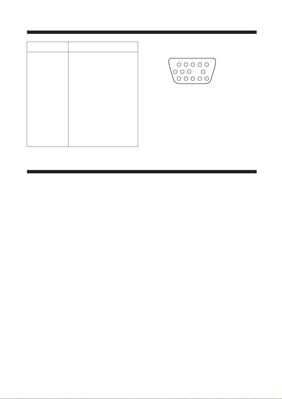
PIN CONNECTOR
Pin Signal
1 Red
2 Green
3 Blue
4 GND
5 GND(Self-Test)
6 GND-Red
7 GND-Green
8 GND-Blue
- No Pin
10 GND-H.Sync
1 1 GND
12 Bi-directional Data (SDA)
13 Horizontal Sync
14 Vertical Sync (VCLK)
15 Data clock (SCL)
1
6
Arrangement of 15-pin D-sub connector
10
15
CAUTIONS FOR ADJUSTMENT AND REPAIR
¡
Degaussing is always required when adjusting purity or convergence.
¡
The white balance adjustment has been done by a color analyzer in factroy. The adjustment procedure, described
in the service manual is made by a visual check.
¡
Allow 20 minutes warm-up time for the display before checking or adjusting only electrical specification or function.
¡
Reform the leadwire after any repair work.
Caution For Servicing
¡
In case of servicing or replacing CRT, high voltage sometimes remains in the anode of the CRT. Completely
discharge high voltage before servicing or replacing CRT to prevent a shock to the serviceman.
8

ALIGNMENT PROCEDURE
Standard Adjustment Conditions
1. Power source voltage : 100~240Vac 50/60Hz
2. Aging : Take at least 20 minutes warm-up time.
3. Signals
Video : Analog 0.7Vpp 75Ω terminal positive polarity
Synchronizing : TTL level Negative/Positive Separate/Composite
Deflection frequency
Horizontal Frequency : 30 KHz - 54KHz
Vertical Frequency : 50Hz - 120Hz
Pre-Adjustment
1. B+ Adjustment
Adjust 27.3Vdc¡ 0.2Vdc between TP1 and ground at 31.5KHz mode, varying VR501.
Main Adjustment
1. Setting the Controls
Set the value of items as following.
Contrast : Max. (OSD value up to MAX)
Brightness : Center (Set the OSD value to center)
2. H.size, V.size, H.phase, V.position, Pincushion, Trapezoid
Receive the cross hatch pattern of Factory preset mode.
H.Size, V.size, H.phase, V.position, Pincushion, Trapezoid are adjusted at each mode.
In Factory, Auto Alignment was done at each mode. Therefore, Factory preset mode has it's
own value according to each control.
3. Focus
(a) Set brightness control to center and contrast control to MAX.
(b) Receive all "H" character pattern of 54KHz mode signal.
(c) Adjust the Focus control of FBT to obtain best Focus (static focus and Dynamic focus).
4. Geometric Distortion Adjustment.
(a) Receive the cross hatch pattern of 54KHz mode signal.
(b) Pin balance, Pin center, Pin corner, Parallelogram are adjusted the best geometric status.
5. White Balance Adjustment
(a) Select 9300¡£K on the OSD Menu.
(b) Receive a cross hatch pattern of 54KHz mode signal by using the signal generator.
(c) Set the brightness control to the center, the contrast control to the maximum and sub contrast
control VR to the center.
(d) Cut off the FBT screen VR.
(e) Set the brightness control to the maximum and receive all the black patterms.
(f) Select the R-BIAS, G-BIAS and B-BIAS on the OSD menu and adjust the DATA +/- key to
get the color coordinates in x=0.281, y=0.311.
(g) Receive al full white pattern.
(h) Select the R-GAIN, G-GAIN and B-GAIN and adjust Data +/- key to get the color coordinates in
x=0.281¡ 0.05, y=0.311¡ 0.05
(i) Set the brightness control to the center and adjust the sub contrast control to get the screen
luminosity to 30t/L(a full white pattern over 30Ft/l).
(j) Check if the x,y coordinates of color analyzer is in X=0.281¡ 0.05, Y=0.311¡ 0.05.
If the color coordinates is out of range, adjust the R. G. B BIAS & GAIN to get the coorinates in
X=0.281, Y=0.311. Make sure that the coordinates is in range by using contrast control.
9

(k) Select 6550¡£K on the OSD Menu and set the color coordinates in X=0.313, Y=0.329 at the maximum
contrast control and center brightness control.
(l) Check if the a full white pattern is over 30Ft/L. If you satisfied with the result, readjust the internal sub contrast
VR.
6. Static Convergence Adjustment
(a) Apply a magenta cross hatch pattern on display
(b) Adjust the focus from the best over all focus on the display.
Also adjust the brightness to the desired condition
(c) Vertical red and blue lines are converged by varying the angle between the two tabs of the 4-pole magnets.
(d) Horizontal red and blue lines are converged by varing the tabs together, keeping the angle between them
constant.
(e) Apply a white cross hatch pattern on display.
(f) Vertical green and magenta lines are converged by varing the the angle between the two tabs of the 6-pole
magnets.
Horizontal green and magenta lines are converged by varing the tabs together, keeping the angle between them
(g)
constant.
10
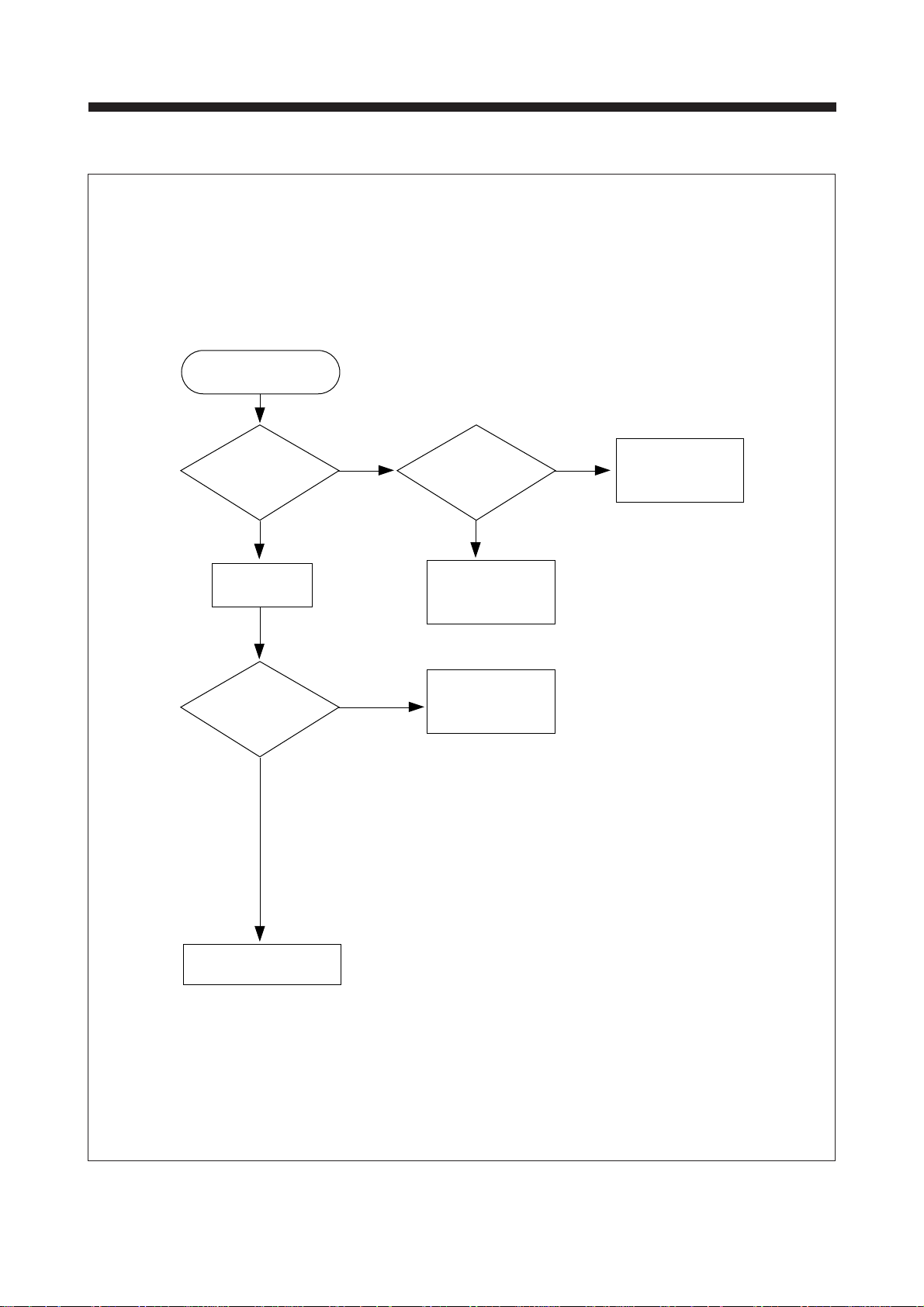
TROUBLESHOOTING HINTS
Yes
Yes
No
About 45Vpp
Yes
No
No
No Character
Are the
Contrast &
Brightness Controls
maximum ?
Is
whole screen
bright?
Is CRT
Cathode (Rk, Gk, Bk)
signal level
normal?
Is
8Vdc line
normal?
Is the
output signal of the
(pin 15, 19, 22) pre-amp
IC801,
normal?
Rk, Gk, Bk
Change the Contrast &
Brightness control value
to maximum
No Raster
Check the peripheral
circuit of CRT
Check the Video output
circuit and IC801
(pin 2, 4, 6) and
their ambient circuit
Refer to
No Raster
Yes
No
No
Trouble in 8Vdc line
of the Main PWB
Check the clamping
pulse circuit
Is
clamping pulse
(pin 23 of IC801)
normal?
No
Check the
signal cable
Is
input signal
normal?
Trouble in IC801 and
its ambient circuit
No
Yes
Yes
Yes
12Vpp
1. No Character
11
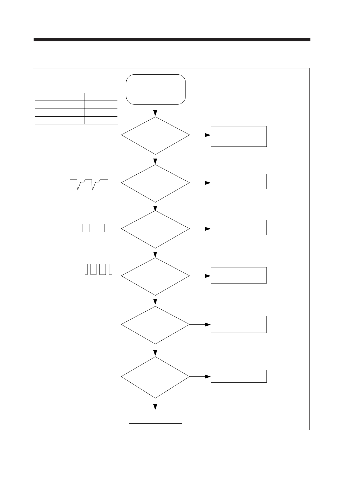
2. No Raster
No
No
Refer to trouble in
power supply unit.
No
No
No
Yes
Yes
Yes
Yes
Yes
Yes
Refer to trouble
in P.S.U
Is
Heater Voltage
(CRT PWB)
about
6V?
Is
CRT heater
red-hot?
Is
whole screen
bright?
Check
G1 voltage about
-70V?
Is CRT
G2 (screen) voltage
about 560V?
Is
65Vdc line
normal?
Yes
Does
increasing of the
Brightness control level
make screen
bright?
No
No
No Raster
Increase the Brightness
& Contrast control level
fully Maxium
Trouble in
power supply
circuit
Trouble in
video
circuit
Trouble in
CRT
Trouble in G1
line of Main
PWB
Trouble in FBT
Trouble in 65Vdc
line of power
supply unit
No High Voltage
trouble in FBT
Raster OK
12
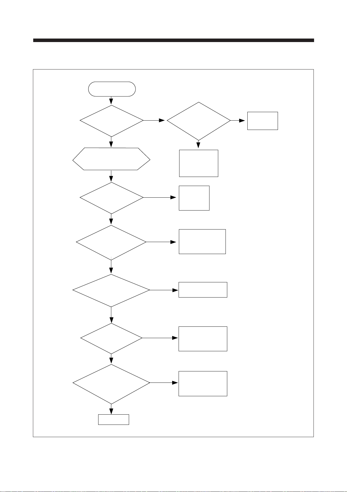
3. A Missing Color
No
No
No
No
RK, GK, BK
About 45V p-p
No
Yes
Yes
Yes
Yes
0.7Vpp
Check video signal
cable or video card.
Trouble in
IC801 or its
ambient circuit
Trouble in G1 line
and G2 line
One color is
missing
Is
input signal
normal?
Is the
output of pre-amp
IC801,
pin 15, 19, 22
all normal?
CRT
Cathode (Rk, Gk, Bk)
is normal?
Each
grid (G1, G2)
voltage
normal?
Is
video output
Q801, Q831, Q861
waveform
normal?
Trouble in
video output
circuit,
Q803, Q804
Q813, Q814
Q823, Q824
or ambient
Trouble in
65/8 Vdc line
Replace CRT
Yes
13
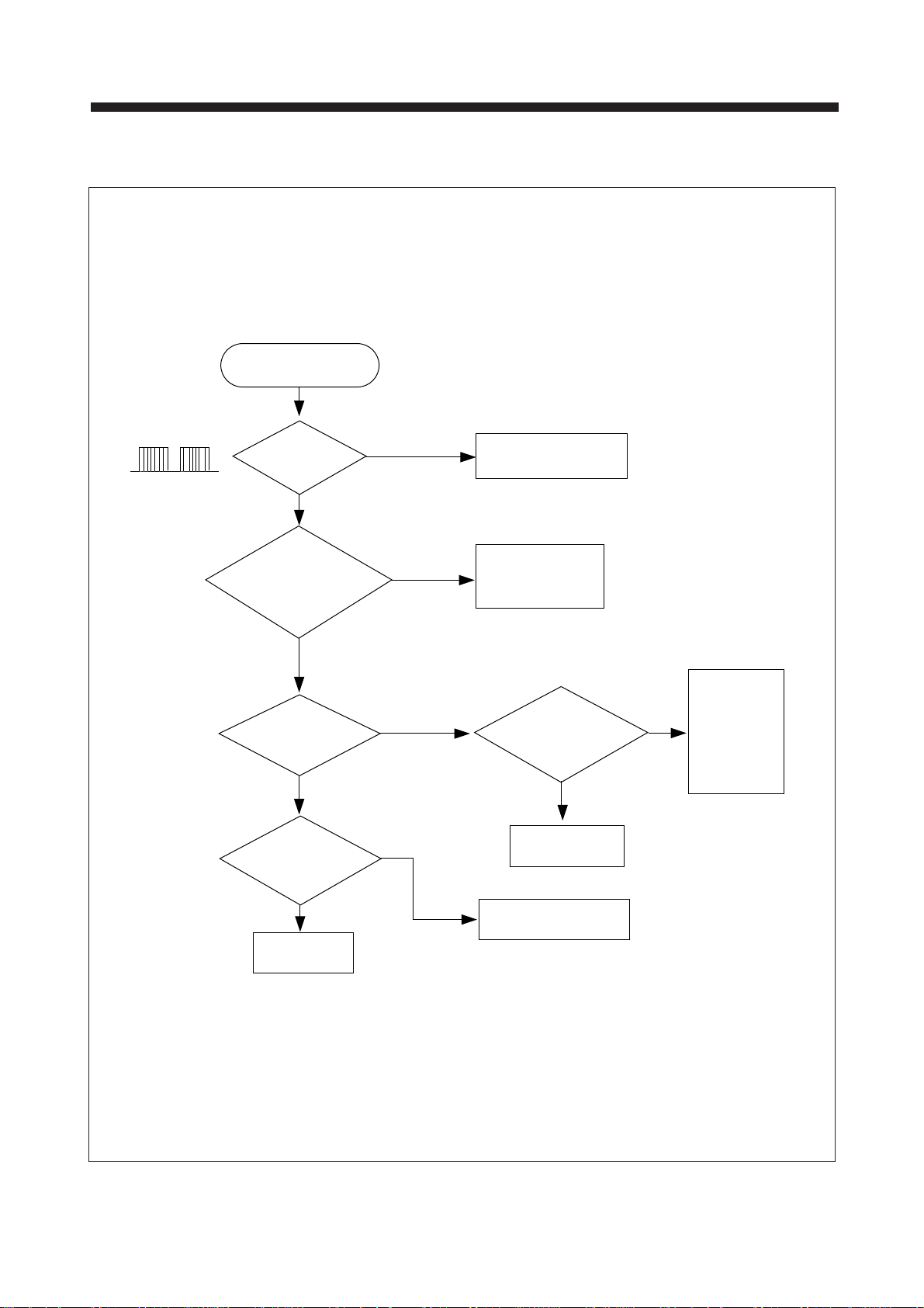
4. Abnormal OSD Font
No
Yes
Yes
Trouble in IC801
and its ambient
circuit
Trouble in IC204
and its ambient
circuit
Trouble in
IC204 or its
ambient circuit
Abnormal OSD Font
Is menu
key selected?
Is OSD Font
exist?
No
Is
the Fast
Blanking signal
(IC204 pin12)
normal?
No
Yes
Is the
output of IC204
(pin 13, 14, 15)
normal?
Yes
One color is
missing
Refer to Missing Color
* If menu key selected.
14
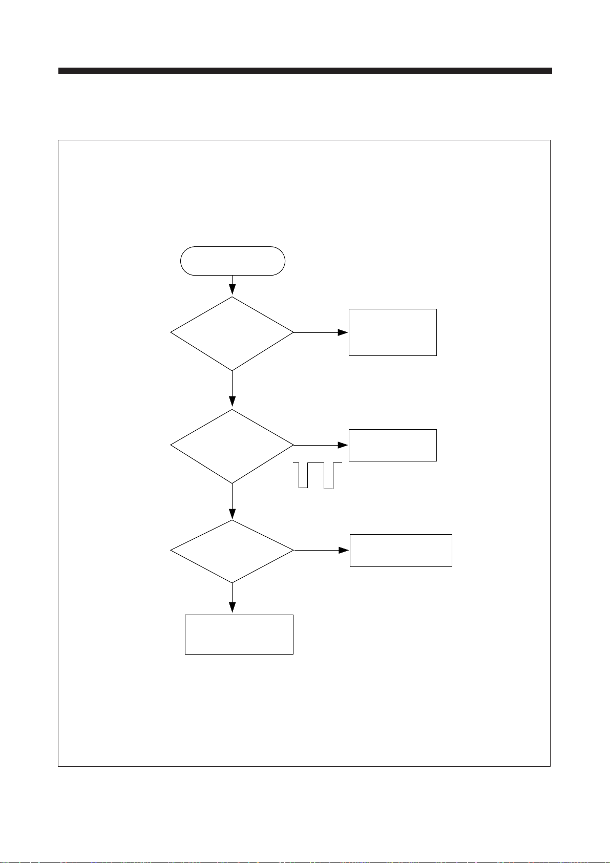
5. Horizontal Output Circuit
11Vp-p
14.5Vp-p
4Vp-p
Yes
Yes
Yes
Yes
Is
B+ line voltage
normal?
Is
Q502 base
waveform
normal?
MODE
VGA
S.VGA
54KHz
No
No
No
Trouble in FBT
No
Refer to trouble
in power supply
unit
Trouble in power
supply circuit
Yes
No
Trouble in Q501, T501
Q501 and its
ambient cirucit
Check the circuit of
P.S.U
No
Trouble in IC501.
Trouble in H.sync line
If the holddown circuit stops the
horizontal oscillator during the check,
turn off the power then turn on again
about 10 seconds later
Trouble in Horizontal
output circuit
(No Raster)
Is
Q501 Gate
waveform
normal?
Is
IC501 7pin
H.DRV waveform
normal?
Is
IC501 pin 9
voltage about
12V?
Yes
Is
the input H.Sync
correct?
B+ Voltage
72Vdc
89Vdc
121Vdc
15
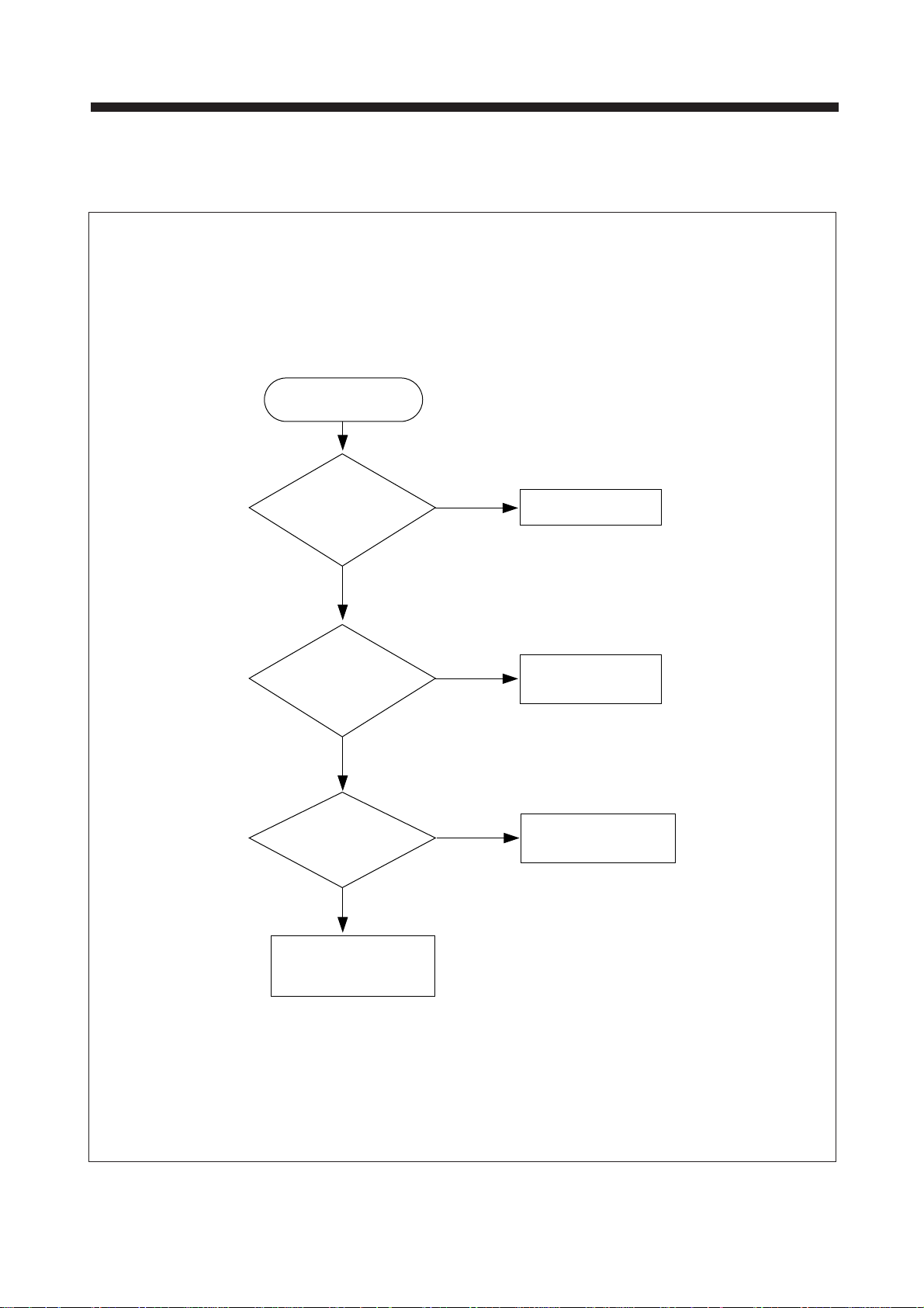
6. Unstable Picture
Yes
No
Trouble in IC501
or its ambient
circuit
Unstable
picture
Is the
pulse of pin 15 of
the IC501
correct?
Yes
No
Check IC201 and
its ambient circuit
Is the
pulse of pin 33 of
the IC201
correct?
Yes
No
Check the IC201 and
its ambient circuit
Is the
input H.Sync
correct?
Trouble in Signal Cable
or 15P D-Sub Connector
5Vpp
6.1 Horizontal
16
6-2.Vertical
Yes
No
Refer to P.S.V
Unstable
picture
Is the
12Vdc
line voltage is
correct?
Yes
No
Trouble in
vertical D.Y
Is the
pulse of pin 4, 6 of
the IC401
correct?
Yes
No
Check the IC401 and
its ambient circuit
Is the output of
pin 12, 13 of IC501
all normal?
Check the IC501 and its
ambient circuit
17

7. Focus
Yes
OK
Check
Focus VR in
FBT
Is
Focus
acceptable?
Monitor remains
unfocused
Trouble in Focus
circuit (FBT)
No
18

8. Convergence
Yes
Yes
No
Is
convergence
on the center area
bad?
Is
convergence on the
fringe area bad?
Poor convergence
Adjust static
convergence
Refer to
Adjustment
procedure of
convergence
Adjust D.Y
Location
19

9. Abnormal Picture
=1100Vp-p
Yes
Is
changeable the
DC level of the base
of Q508?
Is
changeable the
DC level of pin 7 of
the IC201?
Is the
collector pulse
of Q502 correct?
MODE
VGA
Super VGA
54KHz
Yes
Refer to Horizontal Output circuit
Yes
No Yes
Check the Q515,
Q516 and its
ambient circuit
Check the IC201 and
its ambient circuit
Trouble in H.OSC/
Deflection Circuit
Trouble in Horizontal
output circuit
Check the B+ and
anode voltage of CRT.
* Normally anode voltage
of CRT is approximately,
24KV
* Scan B+ are as follow :
No
No
No
Abnormal
H.Size
Is the
cathode waveform
of D506
correct?
B Voltage
72Vdc
89Vdc
121Vdc
50-250Vpp
Trouble in L501,
C523 or their ambient
circuit
+
9.1 Horizontal Size
* At first, adjust controls in the OSD Menu
20

9.2 Vertical Size
Yes
Is
changeable the
DC voltage
of IC201
pin37
Refer to Vertical Output circuit
No
Check the IC201
and its
ambient circuit
Trouble in Vertical
Output Circuit
Abnormal
V.Size
21

10. Side-Pincushion Circuit
Yes
No
O.K
Side-Pincushion distortion
is excessive or barrel
Select
the side-pincushion
icon in OSD menu,
and adjust acceptable
position
Yes
No
Check the Q507, Q510
and its
ambient circuit
Is the
waveform of IC501
(pin 11) correct?
Check the IC501 and
its ambient circuit
22

11. Power Supply Unit (P.S.U)
No
Switch on
No
Yes
Check the power cord outlet
and diode Bridge D001
No
Yes
No
Yes
Yes
Yes
No
No
A
Trouble P.S.U
Is
power switch
on?
Is
fuse F001
O.K?
Is
the IC002
O.K?
Is
voltage of D001
pin 4 130V (270V)?
Is the
waveform T001 pin 5
correct?
Is
voltage of C102
165V DC?
Is
voltage of IC001
pin9 7V~9V DC
Is
voltage of C104
65V DC?
Replace IC002
Trouble in bridge diode
D001 or peripheral
device
Trouble in switching
power transformer T001
or Q001 and its ambient
circuit
Trouble in T001
or D101
No
Trouble in T001 or D102
23

No
Trouble in D104,
T001
Trouble in D106,
Q104 or IC112
Trouble in IC111
D103
P.S.U O.K
Yes
No
No
Yes
Yes
A
Is
voltage of C110
35V DC?
Is voltage
of IC112 pin 3
12V DC?
Is
voltage of
IC111 pin 3
5V DC?
24

OPERATION & ADJUSTMENT
MENU
CONTRAST
BRIGHTNESS
H.POSITION
H.SIZE
V.POSITION
V.SIZE
1024X768 60Hz
50
CONTRAST
BRIGHTNESS
H.POSITION
H.SIZE
V.POSITION
V.SIZE
1024X768 60Hz
50
Color Select
PINCUSHION
TRAPEZOID
COLOR TEMP.
R. GAIN
B. GAIN
DEGAUSSING
RECALL
1024X768 60Hz
50
50
PINCUSHION
TRAPEZOID
COLOR TEMP.
R. GAIN
B. GAIN
DEGAUSSING
RECALL
1024X768 60Hz
USER 9300 6550
EXIT MENUADJUST SELECT
: Launch OSD(On-Screen Display) Menus
: Select the next function
: Select the previous function
: Increase the value of any selected function
: Decrease the value of any selected function
: Exit OSD Menus & Launch OSD Menus, when no OSD
Register Value change
–+
Register Value change
–+
Register Value change
–+
–+
–+
MENU
EXIT
MENU
–
+
MENU
EXIT
OSD OFF
Key Process
25

1. OSD(On-Screen Display) Menu 1
Adjust the contrast of image, the
CONTRAST
50
difference between light and dark areas
on the screen.
BRIGHTNESS
H. POSITION
H. SIZE
V. POSITION
V. SIZE
Adjust the brightness of the entire
display.
50
Adjust the position of the display horizontally
(left or right).
50
Adjust the display width (horizontal size).
50
Adjust the position of the display vertically
(up or down).
50
Adjust the display height (vertical size).
50
26

2. OSD (On-Screen Display) Menu 2
–+–
+
Adjust the left and right margins for more
PINCUSHION
50
convex or more concave margins.
ƒUImage turns to by .
ƒUImage turns to by .
TRAPEZOID
50
COLOR TEMP.
USER 9300 6550
R. GAIN
50
B. GAIN
50
DEGAUSSING
YESNO
RECALL
YESNO
Adjust the trapezoid of the screen by moving
the lines inward or outward.
ƒUImage turns to by .
ƒUImage turns to by .
Choose different preset color temperatures or
set your own customized color parameters.
Adjust the red gain.
Adjust the blue gain.
Degauss the display and restore image quality
Reset the screen to the Factory Preset Display
settings.
27

BLOCK DIAGRAM
28

PCB LAYOUT
Main PCB Solder Side
29

Video PCB Solder Side
30

Main PCB Component Side
31

Video PCB Component Side
32

SCHEMATIC DIAGRAM
33

34

EXPLODED VIEW DIAGRAM
35

REPLACEMENT PARTS LIST
Important Safety Notice
Components identified with the International Symbol have special characteristics important for safety.
When replacing any components, use only manufacturer's specified parts.
Abbreviation of Description
RESISTOR Description
Allowance
F ¡ 1%
J ¡ 5%
K ¡ 10%
M ¡ 20%
G ¡ 2%
Example:
Fig &
Index
R101
CAP ACIT OR Description
Allowance
C ¡ 0.25pF
D ¡ 0.5%
F ¡ 1pF
J ¡ 5%
K ¡ 10%
P ¡ 100% ~ 0%
Z ¡ 80% ~ -
Example:
Fig &
Index
C102 CCXF1H104Z Ceramic 50V Z
C105 CBSLH200J Ceramic 50V J
C402 CCXB1H331K Ceramic 50V K
Part No Description
Resistors
RE-4Z820J Cabron : 82J
Part No Description
Capacitors
36

PART LIST
!
The components identified by mark have special characteristics important for safety and x-ray radiation.
These should be replaced only with the types specified in the parts list.
LOC PART-CODE PART-NAME PART-DESC
10010 PCFMCAG067 COVER FRONT AS CMC-518X
CGND 9970710164 CRT GND AS 0.12*6*16+BL102NG=630
! CRT 9979615003 CDT M36KXU1 10XX61(T)
DG001 5MG0000050 COIL DEGAUSSING HP-1512B
00010 99720183A0 COVER FRONT AS CMC-518B COVER FRONT
00010 9972018300 COVER FRONT FR-ABS GY-258A
00010 2221080957 RESIN ABS LG AF-312 88328B(GY-275A)
00020 9974819900 BUTTON TACT A FR-ABS GY-258A
00010 2221080957 RESIN ABS LG AF-312 88328B(GY-275A)
00030 9974820000 BUTTON TACT B FR-ABS GY-258A
00010 2221080957 RESIN ABS LG AF-312 88328B(GY-275A)
00040 9977915800 LENS LED ACRYL
00050 997601 1800 SPECIAL SCREW 5 TT2 BIN 5*25 MFZN SPW
00060 9976012900 SCREW SPECIAL TT2 HEX 5*25 SCREW+BAND
00070 717340141 1 SCREW TAPPTITE TT2 BIN 4X14 MFZN
00080 4856812001 TIE CABLE NYLON66 DA100
20010 PCMPM1G067 PCB MAIN MANUAL AS CMC-518X
CA201 9970800012 CABLE SIGNAL AS 15P+2C/DDC=1.5M (IVY)
CA202 99707C0006 CONN AS 5264-12+51088-13=330
CA203 9970780024 CONN AS 5264-8+51088-9#24=330
! C001 CL1UC3104M C LINE ACROSS WORLD AC250V 0.1UF M R.47
C004 CEYP2G221Z C ELECTRO 400V SMH 220MF (25.4*40)
! C515 CMXH3C602J C MYLAR BUP 1.6KV 6000PF J
C523 CMXF2D165J C MYLAR 200V MPP 1.6MF J
C526 CMXF2D474J C MYLAR MPP 200V 0.47MF J
C527 CMXF2G474J C MYLAR MPP 400V 0.47MF J
C528 CMXF2D474J C MYLAR MPP 200V 0.47MF J
! D001 DPBS206GU- DIODE BRIDGE PBS206GU
D207 DAL151RGWS LED AL-151RGWS
EMI 9970K00010 CORE FERRITE RING-18
! F001 5F3CB3122L FUSE CERA SEMKO TL 3.15A 250V MF51
GND1 9970710166 CONN AS 35718-0810+1015#18=90
GND2 9970710166 CONN AS 35718-0810+1015#18=90
IC1 12 1K1A7812P1 IC REGULATOR KIA7812PI
IC201 1DWM207--- IC MICOM UM6861A
IC401 PCHBSWG067 HEAT SINK B AS CMC-518X
I401A 1TDA4866-- IC V.OUT TDA4866
37

LOC PART-CODE PART-NAME PART-DESC
I401B 9977012421 HEAT SINK 124 A1050P-H24
I401C 9976012100 SCREW SPECIAL TT2 BIN 3*10 MFZN PW
IC501 1TDA4858-- IC H.OSC TDA4858
L501 5MC0000060 COIL CHOCK TCH-18A
L502 5MH0000059 COIL H-LINEARITY TRL-147
L504 5MC0000061 COIL CHOCK TCH-12A
PR001 DECP AC140M POSISTOR ECPAC140M290
P001 9979500012 RECEPTACLE 02ME4E1/FIL TER EMI
Q001 PCHCSWG067 HEA T SINK C AS CMC-518X
Q001A T2SK2333-- FET 2SK2333
Q001B 9977018772 HEA T SINK 187 A1050P-H24 42X40
Q001C 9976012100 SCREW SPECIAL TT2 BIN 3*10 MFZN PW
! Q502 PCHASWG067 HEAT SINK A AS CMC-518X
D506A DFMP3FU--- DIODE FMP-3FU
D506B 9976012000 SCREW SPECIAL TT2 BIN 3*8 MFZN PW
LOC PART-CODE PART-NAME PART-DESC
Q502A TBU2520DX- TR BU2520DX
Q502B 9977026500 HEA T SINK 265 A1050P-H24 T=1.5
Q510 TBD677A--- TR BD677A
Q506 PCHDSWG067 HEA T SINK D AS CMC-518X
Q506A T1RF630--- FET IRF630
Q506B 9977010803 HEA T SINK D A1050P-H24 EK (39MM)
Q506C 9976012100 SCREW SPECIAL TT2 BIN 3*10 MFZN PW
Q512 T1RF630--- FET IRF630
RL001 5SC0101030 SW RELAY KM1-H12
RL501 5SC0101030 SW RELAY KM1-H12
R004 RX05V333J- R CEMENT 5W 33K OHM J VERTICAL
SW501 5S80303001 SW LEVER P12T21
TH001 DTP8D13--- THERMISTOR TP8D13
! T001 5RM0000085 TRANS SMPS DWT-35A1
! T002 5RY0000003 TRANS SYNC DST-602
! T501 5RD0000034 TRANS DRIVE DDT-130
T502 5RH0000096 FBT FFA81045H
T503 5R Y0000003 TRANS SYNC DST-602
00010 99741 138A0 FRAME AS CMC-518B
00010 99741 13800 FRAME MAIN E.G.I T=0.8
00020 9973723200 SUPPORTER PCB L FR-ABS GY-258A
00010 2221080957 RESIN ABS LG AF-312 88328B(GY-275A)
00030 9973723201 SUPPORTER PCB R FR-ABS GY-258A
38

LOC PART-CODE PART-NAME PART-DESC
00010 2221080957 RESIN ABS LG AF-312 88328B(GY-275A)
00040 9972212100 COVER SIGNAL FR-ABS GY-258A
00010 2221080957 RESIN ABS LG AF-312 88328B(GY-275A)
00050 9977713400 SP ACER CARD NYLON 6.6 DASC-6N
00030 717340101 1 SCREW TAPPTITE TT2 BIN 4X10 MFZN
00040 7S103B4081 SCREW SPECIAL M/C BIN 4*8 MFZN
30010 PCMPJ1G067 PCB SMD AS CMC-518X
C008 HCFK104ZCA C CHIP CERA 50V Y5V 0.1MF Z 2012
C108 HCFK104ZCA C CHIP CERA 50V Y5V 0.1MF Z 2012
C1 17 HCFK104ZCA C CHIP CERA 50V Y5V 0.1MF Z 2012
C1 18 HCFK104ZCA C CHIP CERA 50V Y5V 0.1MF Z 2012
C120 HCFK104ZCA C CHIP CERA 50V Y5V 0.1MF Z 2012
C202 HCFK104ZCA C CHIP CERA 50V Y5V 0.1MF Z 2012
C203 HCFK104ZCA C CHIP CERA 50V Y5V 0.1MF Z 2012
C204 HCFK104ZCA C CHIP CERA 50V Y5V 0.1MF Z 2012
C205 HCFK104ZCA C CHIP CERA 50V Y5V 0.1MF Z 2012
C206 HCQK102JCA C CHIP CERA 50V CH 1000PF J 2012
C209 HCFK104ZCA C CHIP CERA 50V Y5V 0.1MF Z 2012
C21 1 HCFK104ZCA C CHIP CERA 50V Y5V 0.1MF Z 2012
C212 HCFK104ZCA C CHIP CERA 50V Y5V 0.1MF Z 2012
C213 HCFK104ZCA C CHIP CERA 50V Y5V 0.1MF Z 2012
C214 HCFK104ZCA C CHIP CERA 50V Y5V 0.1MF Z 2012
C215 HCFK104ZCA C CHIP CERA 50V Y5V 0.1MF Z 2012
C216 HCFK104ZCA C CHIP CERA 50V Y5V 0.1MF Z 2012
C222 HCFK104ZCA C CHIP CERA 50V Y5V 0.1MF Z 2012
C225 HCFK104ZCA C CHIP CERA 50V Y5V 0.1MF Z 2012
C229 HCFK104ZCA C CHIP CERA 50V Y5V 0.1MF Z 2012
C51 1 HCFK104ZCA C CHIP CERA 50V Y5V 0.1MF Z 2012
C521 HCFK104ZCA C CHIP CERA 50V Y5V 0.1MF Z 2012
C535 HCFK104ZCA C CHIP CERA 50V Y5V 0.1MF Z 2012
C536 HCQK102JCA C CHIP CERA 50V CH 1000PF J 2012
R005 HRFT102JCA R CHIP 1/10 1K OHM J 2012
R006 HRFT564JCA R CHIP 1/10 560K OHM J 2012
R008 HRFT103JCA R CHIP 1/10 10K OHM J 2012
R009 HRFT822JCA R CHIP 1/10 8.2K OHM J 2012
R013 HRFT223JCA R CHIP 1/10 22K OHM J 2012
R014 HRFT102JCA R CHIP 1/10 1K OHM J 2012
R017 HRFT823JCA R CHIP 1/10 82K OHM J 2012
R201 HRFT202JCA R CHIP 1/10 2K OHM J 2012
39

LOC PART-CODE PART-NAME PART-DESC
R203 HRFT202JCA R CHIP 1/10 2K OHM J 2012
R205 HRFT202JCA R CHIP 1/10 2K OHM J 2012
R207 HRFT562JCA R CHIP 1/10 5.6K OHM J 2012
R208 HRFT105JCA R CHIP 1/10 1M OHM J 2012
R209 HRFT562JCA R CHIP 1/10 5.6K OHM J 2012
R210 HRFT562JCA R CHIP 1/10 5.6K OHM J 2012
R21 1 HRFT562JCA R CHIP 1/10 5.6K OHM J 2012
R213 HRFT153JCA R CHIP 1/10 15K OHM J 2012
R214 HRFT153JCA R CHIP 1/10 15K OHM J 2012
R215 HRFT101JCA R CHIP 1/10 100 OHM J 2012
R216 HRFT101JCA R CHIP 1/10 100 OHM J 2012
R221 HRFT103JCA R CHIP 1/10 10K OHM J 2012
R224 HRFT202JCA R CHIP 1/10 2K OHM J 2012
R225 HRFT202JCA R CHIP 1/10 2K OHM J 2012
R226 HRFT202JCA R CHIP 1/10 2K OHM J 2012
R228 HRFT202JCA R CHIP 1/10 2K OHM J 2012
R230 HRFT202JCA R CHIP 1/10 2K OHM J 2012
R232 HRFT202JCA R CHIP 1/10 2K OHM J 2012
R234 HRFT202JCA R CHIP 1/10 2K OHM J 2012
R236 HRFT202JCA R CHIP 1/10 2K OHM J 2012
R238 HRFT472JCA R CHIP 1/10 4.7K OHM J 2012
R240 HRFT472JCA R CHIP 1/10 4.7K OHM J 2012
R242 HRFT202JCA R CHIP 1/10 2K OHM J 2012
R244 HRFT202JCA R CHIP 1/10 2K OHM J 2012
R246 HRFT202JCA R CHIP 1/10 2K OHM J 2012
R248 HRFT562JCA R CHIP 1/10 5.6K OHM J 2012
R249 HRFT202JCA R CHIP 1/10 2K OHM J 2012
R250 HRFT222JCA R CHIP 1/10 2.2K OHM J 2012
R251 HRFT474JCA R CHIP 1/10 470K OHM J 2012
R252 HRFT51 1JCA R CHIP 1/10 510 OHM J 2012
R258 HRFT181JCA R CHIP 1/10 180 OHM J 2012
R263 HRFT101JCA R CHIP 1/10 100 OHM J 2012
R264 HRFT101JCA R CHIP 1/10 100 OHM J 2012
R267 HRFT101JCA R CHIP 1/10 100 OHM J 2012
R268 HRFT101JCA R CHIP 1/10 100 OHM J 2012
R401 HRFT223JCA R CHIP 1/10 22K OHM J 2012
R402 HRFT393JCA R CHIP 1/10 39K OHM J 2012
R403 HRFT393JCA R CHIP 1/10 39K OHM J 2012
R404 HRFT124JCA R CHIP 1/10 120K OHM J 2012
40

LOC PART-CODE PART-NAME PART-DESC
R406 HRFT393JCA R CHIP 1/10 39K OHM J 2012
R407 HRFT393JCA R CHIP 1/10 39K OHM J 2012
R414 HRFT272JCA R CHIP 1/10 2.7K OHM J 2012
R417 HRFT103JCA R CHIP 1/10 10K OHM J 2012
R418 HRFT221JCA R CHIP 1/10 220 OHM J 2012
R502 HRFT153JCA R CHIP 1/10 15K OHM J 2012
R505 HRFT222JCA R CHIP 1/10 2.2K OHM J 2012
R507 HRFT472JCA R CHIP 1/10 4.7K OHM J 2012
R513 HRFT393JCA R CHIP 1/10 39K OHM J 2012
R514 HRFT222JCA R CHIP 1/10 2.2K OHM J 2012
R517 HRFT393JCA R CHIP 1/10 39K OHM J 2012
R524 HRFT222JCA R CHIP 1/10 2.2K OHM J 2012
R525 HRFT102JCA R CHIP 1/10 1K OHM J 2012
R526 HRFT682JCA R CHIP 1/10 6.8K OHM J 2012
R527 HRFT562JCA R CHIP 1/10 5.6K OHM J 2012
R528 HRFT270JCA R CHIP 1/10 27 OHM J 2012
R533 HRFT391JCA R CHIP 1/10 390 OHM J 2012
R537 HRFT513JCA R CHIP 1/10 51K OHM J 2012
R545 HRFT154JCA R CHIP 1/10 150K OHM J 2012
R546 HRFT824JCA R CHIP 1/10 820K OHM J 2012
R547 HRFT912JCA R CHIP 1/10 9.1K OHM J 2012
R549 HRFT153JCA R CHIP 1/10 15K OHM J 2012
R555 HRFT102JCA R CHIP 1/10 1K OHM J 2012
R562 HRFT103JCA R CHIP 1/10 10K OHM J 2012
R563 HRFT122JCA R CHIP 1/10 1.2K OHM J 2012
R564 HRFT273JCA R CHIP 1/10 27K OHM J 2012
R565 HRFT102JCA R CHIP 1/10 1K OHM J 2012
R566 HRFT563JCA R CHIP 1/10 56K OHM J 2012
R567 HRFT104JCA R CHIP 1/10 100K OHM J 2012
R570 HRFT474JCA R CHIP 1/10 470K OHM J 2012
R571 HRFT332JCA R CHIP 1/10 3.3K OHM J 2012
R572 HRFT683JCA R CHIP 1/10 68K OHM J 2012
R573 HRFT243JCA R CHIP 1/10 24K OHM J 2012
R578 HRFT683JCA R CHIP 1/10 68K OHM J 2012
R579 HRFT473JCA R CHIP 1/10 47K OHM J 2012
40010 PCMPJ0G067 PCB MAIN ODD SHAPE A CMC-518X
CW202 485923262S CONN WAFER 5267-05A STICK TYPE
C007 CCYB3A103K C CERA 1KV B 0.01MF K
C014 CCXB3A331K C CERA 1KV B 330PF K (TAPPING)
41

LOC PART-CODE PART-NAME PART-DESC
C018 CH1FDF222M C CERA AC HIKB AC400V 222M
C019 CH1FDF222M C CERA AC HIKB AC400V 222M
C101 CCXB3A101K C CERA 1KV B 100PF K
C102 CEXF2C101V C ELECTRO 160V RSS 100MF (16X25) TP
C103 CCXB3A101K C CERA 1KV B 100PF K
C104 CEYF2A221V C ELECTRO 100V RSS 220MF (16X25)
C106 CEXF1C102C C ELECTRO 16V RUS 1000MF (10X20) TP
C1 10 CEXF1H331C C ELECTRO 50V RUS 330MF 10*20
C1 13 CEXF1E471C C ELECTRO 25V RUS 470MF (10X16) TP
C1 15 CEXF1C102V C ELECTRO 16V RSS 1000MF (10X20) TP
C1 19 CEXF1C471V C ELECTRO 16V RSS 470MF (10X12.5)TP
C405 CEXF1E102C C ELECTRO 25V RUS 1000MF (13X20) TP
C506 CEXF1C102V C ELECTRO 16V RSS 1000MF (10X20) TP
C512 CCXB3A102K C CERA 1KV B 1000PF K (TAPPING)
C516 CMXE2J822J C MYLAR PL 630V 8200PF J
C517 CCXB3D101K C CERA 2KV B 100PF K (TAPPING)
C529 CCXB3A102K C CERA 1KV B 1000PF K (TAPPING)
C530 CEXF2C479V C ELECTRO 160V RSS 4.7MF (8X16) TP
D002 DRGP10D--- DIODE RGP 10-D (T APPING)
D007 DRGP10M--- DIODE RGP10M
D101 DBYT43M--- DIODE BYT43M
D102 DS2L60---R DIODE S2L60
D103 DD2L20U--- DIODE D2L20U
D104 DD1NL40--- DIODE D1NL40
D106 DD2L20U--- DIODE D2L20U
D109 D1N4002A-- DIODE 1N4002
D501 DRGP10D--- DIODE RGP 10-D (T APPING)
D509 DEGP10D--- DIODE EGP10D
D512 DRGP10D--- DIODE RGP 10-D (T APPING)
D519 D1N4004--- DIODE 1N4004
D520 D1N4004--- DIODE 1N4004
D521 D1N4002A-- DIODE 1N4002
D526 DRGP10D--- DIODE RGP 10-D (T APPING)
D527 DRGP10D--- DIODE RGP 10-D (T APPING)
! IC002 1DBL3842-- IC POWER DBL3842
IC203 124LC04B-- IC MEMORY 24LC04B
IC204 1MC141540P IC OSD MC141540P4
P1 4857417500 TERM PIN DA-IB0214(D2.3/DY PIN)
P2 4857417500 TERM PIN DA-IB0214(D2.3/DY PIN)
42

LOC PART-CODE PART-NAME PART-DESC
P3 4857417500 TERM PIN DA-IB0214(D2.3/DY PIN)
P4 4857417500 TERM PIN DA-IB0214(D2.3/DY PIN)
P5 4857417500 TERM PIN DA-IB0214(D2.3/DY PIN)
P6 4857417500 TERM PIN DA-IB0214(D2.3/DY PIN)
R002 RS02Z683J- R M-OXIDE FILM 2W 68K OHM J (TAPPING)
R003 RS01Z473J- R M-OXIDE FILM 1W 47K OHM J (TAPPING)
R015 RW01Z228JN R WIRE WOUND 1W 0.22 OHM J NON-INDUCT
R108 RS01Z390J- R M-OXIDE FILM 1W 39 OHM J (TAPPING)
R410 RS01Z129J- R M-OXIDE FILM 1W 1.2 OHM J (TAPPING)
R41 1 RS01Z109J- R M-OXIDE FILM 1W 1 OHM J (T APPING)
R420 RS02Z159J- R M-OXIDE FILM 2W 1.5 OHM J
R520 RS02Z910J- R M-OXIDE FILM 2W 91 OHM J (TAPPING)
R542 RS01Z331J- R M-OXIDE FILM 1W 330 OHM J (TAPPING)
R568 RS02Z910J- R M-OXIDE FILM 2W 91 OHM J (TAPPING)
R569 RS02Z271J- R M-OXIDE FILM 2W 270 OHM J (TAPPING)
SW201 5S50101Z01 SW T ACT KPT-1115VM 1C-1P
SW202 5S50101Z01 SW T ACT KPT-1115VM 1C-1P
SW203 5S50101Z01 SW T ACT KPT-1115VM 1C-1P
SW204 5S50101Z01 SW T ACT KPT-1115VM 1C-1P
SW205 5S50101Z01 SW T ACT KPT-1115VM 1C-1P
SW206 5S50101Z01 SW T ACT KPT-1115VM 1C-1P
SW207 5S50101Z01 SW T ACT KPT-1115VM 1C-1P
TP101 4857417500 TERM PIN DA-IB0214(D2.3/DY PIN)
TP501 4857417500 TERM PIN DA-IB0214(D2.3/DY PIN)
TP502 4857417500 TERM PIN DA-IB0214(D2.3/DY PIN)
VR001 RV6421202P R SEMI FIXED CCT 065AT 2K OHM B TAP
VR501 RV6121104P R SEMI FIXED CCT 063BT 100K OHM B TAP
VR502 RV6121104P R SEMI FIXED CCT 063BT 100K OHM B TAP
VR503 RV6121502P R SEMI FIXED CCT 063BT 5K OHM B TAP
VR504 RV6121104P R SEMI FIXED CCT 063BT 100K OHM B TAP
50010 PCMPJRG067 PCB MAIN RADIAL AS CMC-518X
C005 CEXF1H470C C ELECTRO 50V RUS 47MF (6.3X1 1) TP
C009 CEXF1H109V C ELECTRO 50V RSS 1MF (5X11) TP
C010 CMXM2A222J C MYLAR 100V 2200PF J (TP)
C01 1 CMXM2A682J C MYLAR 100V 6800PF J (TP)
C012 CMXM2A152J C MYLAR 100V 1500PF J (TP)
C013 CCXB1H102K C CERA 50V B 1000PF K (TAPPING)
C015 CEXF1C101V C ELECTRO 16V RSS 100MF (6.3X11) TP
C016 CEXF1H100V C ELECTRO 50V RSS 10MF (5X11) TP
43

LOC PART-CODE PART-NAME PART-DESC
C107 CEXF1C101C C ELECTRO 16V RUS 100MF (6.3X1 1) TP
C1 14 CEXF1E101C C ELECTRO 25V RUS 100MF (6.3X11) TP
C201 CEXF1H229V C ELECTRO 50V RSS 2.2MF (5X11) TP
C210 CCXB1H102K C CERA 50V B 1000PF K (TAPPING)
C217 CEXF1H479V C ELECTRO 50V RSS 4.7MF (5X11) TP
C218 CEXF1H479V C ELECTRO 50V RSS 4.7MF (5X11) TP
C219 CEXF1H479V C ELECTRO 50V RSS 4.7MF (5X11) TP
C220 CEXF1H229V C ELECTRO 50V RSS 2.2MF (5X11) TP
C221 CEXF1H479V C ELECTRO 50V RSS 4.7MF (5X11) TP
C223 CEXF1H100V C ELECTRO 50V RSS 10MF (5X11) TP
C224 CEXF1C101V C ELECTRO 16V RSS 100MF (6.3X11) TP
C226 CCXB1H103K C CERA 50V B 0.01MF K
C227 CXCH1H330J C CERA 50V CH 33PF J (TAPPING)
C228 CXCH1H330J C CERA 50V CH 33PF J (TAPPING)
C230 CCXB1H101K C CERA 50V B 100PF K (TAPPING)
C231 CCXB1H101K C CERA 50V B 100PF K (TAPPING)
C232 CMXM2A103J C MYLAR 100V 0.01MF J (TP)
C234 CCXB1H102K C CERA 50V B 1000PF K (TAPPING)
C235 CCXB1H181K C CERA 50V B 180PF K (TAPPING)
C236 CCXB1H181K C CERA 50V B 180PF K (TAPPING)
C401 CMXM2A104J C MYLAR 100V 0.1MF J (TP)
C402 CMXM2A104J C MYLAR 100V 0.1MF J (TP)
C403 CMXM2A223J C MYLAR 100V 0.022MF J TP
C404 CMXM2A223J C MYLAR 100V 0.022MF J TP
C406 CMXM2A104J C MYLAR 100V 0.1MF J (TP)
C407 CEXF1H101V C ELECTRO 50V RSS 100MF (8X11.5) TP
C408 CCXB1H102K C CERA 50V B 1000PF K (TAPPING)
C409 CMXM2D104J C MYLAR 200V 0.1MF J
C410 CCXB2H471K C CERA 500V B 470PF K (TAPPING)
C41 1 CMXM2A104J C MYLAR 100V 0.1MF J (TP)
C501 CXCH1H470J C CERA 50V CH 47PF J (TAPPING)
C502 CEXF1H100V C ELECTRO 50V RSS 10MF (5X11) TP
C503 CEXF1H100V C ELECTRO 50V RSS 10MF (5X11) TP
C504 CEXF1H220V C ELECTRO 50V RSS 22MF (5X11) TP
C505 CMXM2A472J C MYLAR 100V 4700PF J (TP)
C507 CMXM2A123J C MYLAR 100V 0.012MF J (TP)
C508 CMXM2A103J C MYLAR 100V 0.01MF J (TP)
C509 CMXM2A102J C MYLAR 100V 1000PF J (TP)
C510 CMXM2A473J C MYLAR 100V 0.047MF J (TP)
44

LOC PART-CODE PART-NAME PART-DESC
C513 CMXM2A104J C MYLAR 100V 0.1MF J (TP)
C514 CMXM2A103J C MYLAR 100V 0.01MF J (TP)
C518 CMXM2A472J C MYLAR 100V 4700PF J (TP)
C519 CCXB1H222K C CERA 50V B 2200PF K (TAPPING)
C520 CEXF1H100V C ELECTRO 50V RSS 10MF (5X11) TP
C522 CCXB1H103K C CERA 50V B 0.01MF K
C524 CCXB2H102K C CERA 500V B 1000PF K (TAPPING)
C525 CCXB1H103K C CERA 50V B 0.01MF K
C531 CMXM2A682J C MYLAR 100V 6800PF J (TP)
C532 CMXM2A103J C MYLAR 100V 0.01MF J (TP)
C533 CEXF1H220V C ELECTRO 50V RSS 22MF (5X11) TP
C534 CEXF1C101V C ELECTRO 16V RSS 100MF (6.3X11) TP
C537 CMXM2A152J C MYLAR 100V 1500PF J (TP)
C538 CEXF2V109V C ELECTRO 350V RSS 1MF(8*11.5)
C539 CEXF1E101C C ELECTRO 25V RUS 100MF (6.3X11) TP
C540 CEXF1E101C C ELECTRO 25V RUS 100MF (6.3X11) TP
C541 CMXM2A104J C MYLAR 100V 0.1MF J (TP)
F001A 4857415000 FUSE CLIP BSP3-H T0.4 SN 5.2
F001B 4857415000 FUSE CLIP BSP3-H T0.4 SN 5.2
IC1 11 1XC62A500- IC REGULAT OR XC62AP5002TH
IC202 1KA7542--- IC VOTAGE DETECTOR KA7542
Q002 TZTC3198Y - TR KTC3198Y-(1815Y) (AUT O)
Q101 TKTA1273Y- TR KTA1273-Y
Q102 TZTC3198Y - TR KTC3198Y-(1815Y) (AUT O)
Q104 TKTA1273Y- TR KTA1273-Y
Q105 TZTC3198Y - TR KTC3198Y-(1815Y) (AUT O)
Q106 TZTC3198Y - TR KTC3198Y-(1815Y) (AUT O)
Q201 TZTA1270Y- TR KTA1270Y(AUTO)(562Y)
Q202 TZTC3198Y - TR KTC3198Y-(1815Y) (AUT O)
Q203 TZTC3198Y - TR KTC3198Y-(1815Y) (AUT O)
Q401 TZTC3198Y - TR KTC3198Y-(1815Y) (AUT O)
Q501 TBSN254A-- FET TBSN254A
Q503 TZTC3198Y - TR KTC3198Y-(1815Y) (AUT O)
Q504 TZTC3198Y - TR KTC3198Y-(1815Y) (AUT O)
Q505 TZTA1270Y- TR KTA1270Y(AUTO)(562Y)
Q507 TZTA1270Y- TR KTA1270Y(AUTO)(562Y)
Q508 TZTA1270Y- TR KTA1270Y(AUTO)(562Y)
Q51 1 TZTC3207-- TR KTC3207 (AUTO)
Q513 TZTC3198Y - TR KTC3198Y-(1815Y) (AUT O)
45

LOC PART-CODE PART-NAME PART-DESC
Q514 TZTC3198Y - TR KTC3198Y-(1815Y) (AUT O)
Q515 TZTC3198Y - TR KTC3198Y-(1815Y) (AUT O)
Q516 TZTA1270Y- TR KTA1270Y(AUTO)(562Y)
Q518 TZTC3198Y - TR KTC3198Y-(1815Y) (AUT O)
Q520 TKTA1277Y- TR KTA1277Y
Q521 TZTC3206Y - TR KTC3206Y (2229Y)
Q522 TZTA1270Y- TR KTA1270Y(AUTO)(562Y)
Q523 TZTC3198Y - TR KTC3198Y-(1815Y) (AUT O)
Q524 TZTC3198Y - TR KTC3198Y-(1815Y) (AUT O)
Q525 TZTC3198Y - TR KTC3198Y-(1815Y) (AUT O)
Q526 TZTC3198Y - TR KTC3198Y-(1815Y) (AUT O)
X201 5PEF0EC8T4 RESONATOR EFOEC8004T4
60010 PCMPJAG067 PCB MAIN AXIAL AS CMC-518X
BD001 5PB13890-- COIL BEAD BI3890
BD002 5PB13857-- COIL BEAD BI3857(AXIAL)
BD003 5PB13857-- COIL BEAD BI3857(AXIAL)
BD004 5PB13890-- COIL BEAD BI3890
BD005 5PB13857-- COIL BEAD BI3857(AXIAL)
BD006 5PB13857-- COIL BEAD BI3857(AXIAL)
BD202 5PB13857-- COIL BEAD BI3857(AXIAL)
BD203 5PB13857-- COIL BEAD BI3857(AXIAL)
BD501 5PB13857-- COIL BEAD BI3857(AXIAL)
BD502 5PB13857-- COIL BEAD BI3857(AXIAL)
BD503 5PB13857-- COIL BEAD BI3857(AXIAL)
DZ001 DDZ7R5BM-- DIODE ZENER DZ7.5BM
DZ003 DDZ22BM--- DIODE ZENER DZ22BM
DZ006 DDZ22BM--- DIODE ZENER DZ22BM
DZ107 DDZ8R2BM-- DIODE ZENER DZ8.2BM
DZ201 DDZ5R1B--- DIODE ZENER DZ-5.1B
DZ202 DDZ5R1B--- DIODE ZENER DZ-5.1B
DZ203 DDZ5R1B--- DIODE ZENER DZ-5.1B
DZ204 DDZ5R1B--- DIODE ZENER DZ-5.1B
DZ205 DDZ5R1B--- DIODE ZENER DZ-5.1B
DZ206 DDZ5R1B--- DIODE ZENER DZ-5.1B
DZ510 DDZ15BM--- DIODE ZENER DZ15BM
DZ514 DDZ5R1B--- DIODE ZENER DZ-5.1B
D004 DZN4148--- DIODE 1N4148 AUTO 52MM
D005 DZN4148--- DIODE 1N4148 AUTO 52MM
D108 DZN4148--- DIODE 1N4148 AUTO 52MM
46

LOC PART-CODE PART-NAME PART-DESC
D206 DZN4148--- DIODE 1N4148 AUTO 52MM
D210 DZN4148--- DIODE 1N4148 AUTO 52MM
D21 1 DZN4148--- DIODE 1N4148 AUTO 52MM
D212 DZN4148--- DIODE 1N4148 AUTO 52MM
D213 DZN4148--- DIODE 1N4148 AUTO 52MM
D214 DZN4148--- DIODE 1N4148 AUTO 52MM
D502 DZN4148--- DIODE 1N4148 AUTO 52MM
D504 DZN4148--- DIODE 1N4148 AUTO 52MM
D505 DZN4148--- DIODE 1N4148 AUTO 52MM
D507 DZN4148--- DIODE 1N4148 AUTO 52MM
D508 DZN4148--- DIODE 1N4148 AUTO 52MM
D510 DZN4148--- DIODE 1N4148 AUTO 52MM
D51 1 DZN4148--- DIODE 1N4148 AUTO 52MM
D517 DZN4148--- DIODE 1N4148 AUTO 52MM
D518 DZN4148--- DIODE 1N4148 AUTO 52MM
D524 DZN4148--- DIODE 1N4148 AUTO 52MM
D525 DZN4148--- DIODE 1N4148 AUTO 52MM
D528 DZN4148--- DIODE 1N4148 AUTO 52MM
D529 DZN4148--- DIODE 1N4148 AUTO 52MM
D531 DZN4148--- DIODE 1N4148 AUTO 52MM
E1 4856310200 EYE LET BSR T0.2 (R2.0)
E10 4856310200 EYE LET BSR T0.2 (R2.0)
E1 1 4856310300 EYE LET BSR T0.2 (R1.6)
E12 4856310300 EYE LET BSR T0.2 (R1.6)
E13 4856310300 EYE LET BSR T0.2 (R1.6)
E14 4856310300 EYE LET BSR T0.2 (R1.6)
E15 4856310300 EYE LET BSR T0.2 (R1.6)
E16 4856310300 EYE LET BSR T0.2 (R1.6)
E17 4856310300 EYE LET BSR T0.2 (R1.6)
E18 4856310300 EYE LET BSR T0.2 (R1.6)
E2 4856310200 EYE LET BSR T0.2 (R2.0)
E3 4856310200 EYE LET BSR T0.2 (R2.0)
E4 4856310200 EYE LET BSR T0.2 (R2.0)
E5 4856310200 EYE LET BSR T0.2 (R2.0)
E6 4856310200 EYE LET BSR T0.2 (R2.0)
E7 4856310200 EYE LET BSR T0.2 (R2.0)
E8 4856310200 EYE LET BSR T0.2 (R2.0)
E9 4856310200 EYE LET BSR T0.2 (R2.0)
J001 85801052GY WIRE COPPER 1/0.52 TIN COATING
47

LOC PART-CODE PART-NAME PART-DESC
J003 85801052GY WIRE COPPER 1/0.52 TIN COATING
J014 85801052GY WIRE COPPER 1/0.52 TIN COATING
J101 85801052GY WIRE COPPER 1/0.52 TIN COATING
J102 85801052GY WIRE COPPER 1/0.52 TIN COATING
J103 85801052GY WIRE COPPER 1/0.52 TIN COATING
J105 85801052GY WIRE COPPER 1/0.52 TIN COATING
J106 85801052GY WIRE COPPER 1/0.52 TIN COATING
J107 85801052GY WIRE COPPER 1/0.52 TIN COATING
J108 85801052GY WIRE COPPER 1/0.52 TIN COATING
J109 85801052GY WIRE COPPER 1/0.52 TIN COATING
J1 10 85801052GY WIRE COPPER 1/0.52 TIN COATING
J1 11 85801052GY WIRE COPPER 1/0.52 TIN COATING
J1 12 85801052GY WIRE COPPER 1/0.52 TIN COATING
J1 13 85801052GY WIRE COPPER 1/0.52 TIN COATING
J1 14 85801052GY WIRE COPPER 1/0.52 TIN COATING
J1 15 85801052GY WIRE COPPER 1/0.52 TIN COATING
J1 18 85801052GY WIRE COPPER 1/0.52 TIN COATING
J1 19 85801052GY WIRE COPPER 1/0.52 TIN COATING
J120 85801052GY WIRE COPPER 1/0.52 TIN COATING
J121 85801052GY WIRE COPPER 1/0.52 TIN COATING
J122 85801052GY WIRE COPPER 1/0.52 TIN COATING
J123 85801052GY WIRE COPPER 1/0.52 TIN COATING
J124 85801052GY WIRE COPPER 1/0.52 TIN COATING
J125 85801052GY WIRE COPPER 1/0.52 TIN COATING
J126 85801052GY WIRE COPPER 1/0.52 TIN COATING
J127 85801052GY WIRE COPPER 1/0.52 TIN COATING
J128 85801052GY WIRE COPPER 1/0.52 TIN COATING
J129 85801052GY WIRE COPPER 1/0.52 TIN COATING
J130 85801052GY WIRE COPPER 1/0.52 TIN COATING
J131 85801052GY WIRE COPPER 1/0.52 TIN COATING
J132 85801052GY WIRE COPPER 1/0.52 TIN COATING
J133 85801052GY WIRE COPPER 1/0.52 TIN COATING
J134 85801052GY WIRE COPPER 1/0.52 TIN COATING
J136 85801052GY WIRE COPPER 1/0.52 TIN COATING
J137 85801052GY WIRE COPPER 1/0.52 TIN COATING
J139 85801052GY WIRE COPPER 1/0.52 TIN COATING
J140 85801052GY WIRE COPPER 1/0.52 TIN COATING
J141 85801052GY WIRE COPPER 1/0.52 TIN COATING
J142 85801052GY WIRE COPPER 1/0.52 TIN COATING
48

LOC PART-CODE PART-NAME PART-DESC
J143 85801052GY WIRE COPPER 1/0.52 TIN COATING
J144 85801052GY WIRE COPPER 1/0.52 TIN COATING
J145 85801052GY WIRE COPPER 1/0.52 TIN COATING
J146 85801052GY WIRE COPPER 1/0.52 TIN COATING
J147 85801052GY WIRE COPPER 1/0.52 TIN COATING
J148 85801052GY WIRE COPPER 1/0.52 TIN COATING
J149 85801052GY WIRE COPPER 1/0.52 TIN COATING
J150 85801052GY WIRE COPPER 1/0.52 TIN COATING
J151 85801052GY WIRE COPPER 1/0.52 TIN COATING
J152 85801052GY WIRE COPPER 1/0.52 TIN COATING
J153 85801052GY WIRE COPPER 1/0.52 TIN COATING
J154 85801052GY WIRE COPPER 1/0.52 TIN COATING
J155 85801052GY WIRE COPPER 1/0.52 TIN COATING
J156 85801052GY WIRE COPPER 1/0.52 TIN COATING
J157 85801052GY WIRE COPPER 1/0.52 TIN COATING
J158 85801052GY WIRE COPPER 1/0.52 TIN COATING
J159 85801052GY WIRE COPPER 1/0.52 TIN COATING
J160 85801052GY WIRE COPPER 1/0.52 TIN COATING
J161 85801052GY WIRE COPPER 1/0.52 TIN COATING
J162 85801052GY WIRE COPPER 1/0.52 TIN COATING
J163 85801052GY WIRE COPPER 1/0.52 TIN COATING
J164 85801052GY WIRE COPPER 1/0.52 TIN COATING
J165 85801052GY WIRE COPPER 1/0.52 TIN COATING
J166 85801052GY WIRE COPPER 1/0.52 TIN COATING
J167 85801052GY WIRE COPPER 1/0.52 TIN COATING
J168 85801052GY WIRE COPPER 1/0.52 TIN COATING
J169 85801052GY WIRE COPPER 1/0.52 TIN COATING
J170 85801052GY WIRE COPPER 1/0.52 TIN COATING
J171 85801052GY WIRE COPPER 1/0.52 TIN COATING
J172 85801052GY WIRE COPPER 1/0.52 TIN COATING
J173 85801052GY WIRE COPPER 1/0.52 TIN COATING
J174 85801052GY WIRE COPPER 1/0.52 TIN COATING
J176 85801052GY WIRE COPPER 1/0.52 TIN COATING
J177 85801052GY WIRE COPPER 1/0.52 TIN COATING
J178 85801052GY WIRE COPPER 1/0.52 TIN COATING
J179 85801052GY WIRE COPPER 1/0.52 TIN COATING
J180 85801052GY WIRE COPPER 1/0.52 TIN COATING
J181 85801052GY WIRE COPPER 1/0.52 TIN COATING
J182 85801052GY WIRE COPPER 1/0.52 TIN COATING
49

LOC PART-CODE PART-NAME PART-DESC
J183 85801052GY WIRE COPPER 1/0.52 TIN COATING
J184 85801052GY WIRE COPPER 1/0.52 TIN COATING
J185 85801052GY WIRE COPPER 1/0.52 TIN COATING
J186 85801052GY WIRE COPPER 1/0.52 TIN COATING
J187 85801052GY WIRE COPPER 1/0.52 TIN COATING
J188 85801052GY WIRE COPPER 1/0.52 TIN COATING
J189 85801052GY WIRE COPPER 1/0.52 TIN COATING
J190 85801052GY WIRE COPPER 1/0.52 TIN COATING
J191 85801052GY WIRE COPPER 1/0.52 TIN COATING
J192 85801052GY WIRE COPPER 1/0.52 TIN COATING
J193 85801052GY WIRE COPPER 1/0.52 TIN COATING
J194 85801052GY WIRE COPPER 1/0.52 TIN COATING
J195 85801052GY WIRE COPPER 1/0.52 TIN COATING
J196 85801052GY WIRE COPPER 1/0.52 TIN COATING
J197 85801052GY WIRE COPPER 1/0.52 TIN COATING
J198 85801052GY WIRE COPPER 1/0.52 TIN COATING
J199 85801052GY WIRE COPPER 1/0.52 TIN COATING
J200 85801052GY WIRE COPPER 1/0.52 TIN COATING
J201 85801052GY WIRE COPPER 1/0.52 TIN COATING
J204 85801052GY WIRE COPPER 1/0.52 TIN COATING
J205 85801052GY WIRE COPPER 1/0.52 TIN COATING
L201 5CPZ151K03 COIL PEAKING 150UH 7MM K (LAL03TB)
L202 5CPZ568K03 COIL PEAKING 0.56UH 7MM K(LAL03TB)
L503 5CPZ680K04 COIL PEAKING 68UH K 10.5MM (LA04TB)
R001 RD-2Z684J- R CARBON FILM 1/2 680K OHM J
R007 RD-AZ912J- R CARBON FILM 1/6 9.1K OHM J
R010 RD-AZ563J- R CARBON FILM 1/6 56K OHM J
R01 1 RD-4Z564J- R CARBON FILM 1/4 560K OHM J
R012 RD-AZ220J- R CARBON FILM 1/6 22 OHM J
R016 RD-AZ103J- R CARBON FILM 1/6 10K OHM J
R020 RC-2Z565J- R CARBON COMP 1/2 5.6M OHM J
R022 RD-4Z564J- R CARBON FILM 1/4 560K OHM J
R101 RD-4Z154J- R CARBON FILM 1/4 150K OHM J
R102 RD-2Z241J- R CARBON FILM 1/2 240 OHM J
R103 RD-4Z331J- R CARBON FILM 1/4 330 OHM J
R104 RD-AZ103J- R CARBON FILM 1/6 10K OHM J
R105 RD-2Z221J- R CARBON FILM 1/2 220 OHM J
R106 RD-4Z102J- R CARBON FILM 1/4 1K OHM J
R107 RD-AZ103J- R CARBON FILM 1/6 10K OHM J
50

LOC PART-CODE PART-NAME PART-DESC
R109 RD-AZ102J- R CARBON FILM 1/6 1K OHM J
R1 10 RD-4Z101J- R CARBON FILM 1/4 100 OHM J
R1 11 RD-AZ102J- R CARBON FILM 1/6 1K OHM J
R202 RD-AZ393J- R CARBON FILM 1/6 39K OHM J
R204 RD-AZ393J- R CARBON FILM 1/6 39K OHM J
R206 RD-AZ183J- R CARBON FILM 1/6 18K OHM J
R217 RD-AZ623J- R CARBON FILM 1/6 62K OHM J
R218 RD-AZ103J- R CARBON FILM 1/6 10K OHM J
R219 RD-AZ223J- R CARBON FILM 1/6 22K OHM J
R220 RD-AZ221J- R CARBON FILM 1/6 220 OHM J
R222 RD-AZ221J- R CARBON FILM 1/6 220 OHM J
R227 RD-AZ393J- R CARBON FILM 1/6 39K OHM J
R229 RD-AZ393J- R CARBON FILM 1/6 39K OHM J
R231 RD-AZ393J- R CARBON FILM 1/6 39K OHM J
R233 RD-AZ393J- R CARBON FILM 1/6 39K OHM J
R235 RD-AZ393J- R CARBON FILM 1/6 39K OHM J
R237 RD-AZ823J- R CARBON FILM 1/6 82K OHM J
R239 RD-AZ103J- R CARBON FILM 1/6 10K OHM J
R241 RD-AZ472J- R CARBON FILM 1/6 4.7K OHM J
R243 RD-AZ512J- R CARBON FILM 1/6 5.1K OHM J
R245 RD-AZ183J- R CARBON FILM 1/6 18K OHM J
R247 RD-AZ123J- R CARBON FILM 1/6 12K OHM J
R253 RD-AZ471J- R CARBON FILM 1/6 470 OHM J
R254 RD-AZ333J- R CARBON FILM 1/6 33K OHM J
R255 RD-AZ101J- R CARBON FILM 1/6 100 OHM J
R256 RD-AZ101J- R CARBON FILM 1/6 100 OHM J
R257 RD-AZ101J- R CARBON FILM 1/6 100 OHM J
R259 RD-4Z621J- R CARBON FILM 1/4 620 OHM J
R260 RD-AZ101J- R CARBON FILM 1/6 100 OHM J
R261 RD-AZ623J- R CARBON FILM 1/6 62K OHM J
R262 RD-AZ223J- R CARBON FILM 1/6 22K OHM J
R265 RD-AZ103J- R CARBON FILM 1/6 10K OHM J
R266 RD-AZ472J- R CARBON FILM 1/6 4.7K OHM J
R405 RD-AZ273J- R CARBON FILM 1/6 27K OHM J
R408 RD-AZ102J- R CARBON FILM 1/6 1K OHM J
R409 RD-AZ102J- R CARBON FILM 1/6 1K OHM J
R412 RD-2Z100J- R CARBON FILM 1/2 10 OHM J
R413 RD-2Z221J- R CARBON FILM 1/2 220 OHM J
R415 RD-2Z100J- R CARBON FILM 1/2 10 OHM J
51

LOC PART-CODE PART-NAME PART-DESC
R416 RD-4Z363J- R CARBON FILM 1/4 36K OHM J
R419 RD-AZ471J- R CARBON FILM 1/6 470 OHM J
R421 RD-AZ243J- R CARBON FILM 1/6 24K OHM J
R422 RD-AZ912J- R CARBON FILM 1/6 9.1K OHM J
R501 RD-AZ122J- R CARBON FILM 1/6 1.2K OHM J
R503 RD-AZ623J- R CARBON FILM 1/6 62K OHM J
R504 RD-4Z274J- R CARBON FILM 1/4 270K OHM J
R506 RD-AZ222J- R CARBON FILM 1/6 2.2K OHM J
R508 RD-2Z100J- R CARBON FILM 1/2 10 OHM J
R509 RD-AZ102J- R CARBON FILM 1/6 1K OHM J
R51 1 RD-AZ103J- R CARBON FILM 1/6 10K OHM J
R515 RD-AZ122J- R CARBON FILM 1/6 1.2K OHM J
R516 RD-AZ362J- R CARBON FILM 1/6 3.6K OHM J
R518 RD-AZ220J- R CARBON FILM 1/6 22 OHM J
R519 RD-2Z221J- R CARBON FILM 1/2 220 OHM J
R521 RD-AZ184J- R CARBON FILM 1/6 180K OHM J
R522 RD-AZ474J- R CARBON FILM 1/6 470K OHM J
R523 RD-AZ103J- R CARBON FILM 1/6 10K OHM J
R529 RD-AZ622J- R CARBON FILM 1/6 6.2K OHM J
R530 RD-AZ102J- R CARBON FILM 1/6 1K OHM J
R531 RD-AZ682J- R CARBON FILM 1/6 6.8K OHM J
R532 RD-AZ471J- R CARBON FILM 1/6 470 OHM J
R534 RD-AZ333J- R CARBON FILM 1/6 33K OHM J
R535 RD-AZ124J- R CARBON FILM 1/6 120K OHM J
R536 RD-AZ102J- R CARBON FILM 1/6 1K OHM J
R538 RD-AZ563J- R CARBON FILM 1/6 56K OHM J
R539 RD-AZ223J- R CARBON FILM 1/6 22K OHM J
R540 RD-4Z104J- R CARBON FILM 1/4 100K OHM J
R541 RD-4Z104J- R CARBON FILM 1/4 100K OHM J
R543 RD-4Z101J- R CARBON FILM 1/4 100 OHM J
R544 RD-AZ102J- R CARBON FILM 1/6 1K OHM J
R548 RD-AZ433J- R CARBON FILM 1/6 43K OHM J
R550 RD-AZ623J- R CARBON FILM 1/6 62K OHM J
R551 RD-AZ242J- R CARBON FILM 1/6 2.4K OHM J
R552 RD-AZ122J- R CARBON FILM 1/6 1.2K OHM J
R554 RD-4Z153J- R CARBON FILM 1/4 15K OHM J
R556 RD-AZ472J- R CARBON FILM 1/6 4.7K OHM J
R557 RD-AZ151J- R CARBON FILM 1/6 150 OHM J
R558 RD-AZ222J- R CARBON FILM 1/6 2.2K OHM J
52

LOC PART-CODE PART-NAME PART-DESC
R561 RD-AZ102J- R CARBON FILM 1/6 1K OHM J
R574 RD-AZ103J- R CARBON FILM 1/6 10K OHM J
R575 RD-AZ103J- R CARBON FILM 1/6 10K OHM J
00001 9979800453 PCB MAIN T1.6*330*246
30020 PCCTSWG067 PCB CRT AS CMC-518X
BD894 5MBFD3512R EMI BEAD FILTER BFD 3512 R2
CA801 9970710165 CONN AS 35718-0810+1015#22=160
CW801 9979220021 CONN WAFER SMAW250-06 (ANGLE)
CW802 9979200216 CONN WAFER 5268-12A
CW803 4859234320 CONN WAFER 5268-08A
CW804 9979300002 SOCKET CRT ISHM10S
C898 CCXE3D103P C CERA HIKE 2KV 0.01MF P
IC801 1MC13282EP IC VIDEO PREAMP MC13282EP
Q801 TBFQ225--- TR BFQ225
Q831 TBFQ225--- TR BFQ225
Q861 TBFQ225--- TR BFQ225
SG891 ZEW295804A SPARK GAP S-23 1KV (LEAD 4.5M/M)
00010 9977241 100 SHIELD CASE SPTH-C T=0.3
00020 9977241200 SHIELD COVER SPTH-C T=0.3
00030 9977713400 SP ACER CARD NYLON 6.6 DASC-6N
00040 9975816100 LABEL DHHS STICKER 120P*70*45
40010 PCCTJ1G067 PCB CRT CHIP AS CMC-518X
C801 HCFK104ZCA C CHIP CERA 50V Y5V 0.1MF Z 2012
C802 HCFK104ZCA C CHIP CERA 50V Y5V 0.1MF Z 2012
C803 HCFK104ZCA C CHIP CERA 50V Y5V 0.1MF Z 2012
C804 HCFK104ZCA C CHIP CERA 50V Y5V 0.1MF Z 2012
C812 HCFK104ZCA C CHIP CERA 50V Y5V 0.1MF Z 2012
C831 HCFK104ZCA C CHIP CERA 50V Y5V 0.1MF Z 2012
C832 HCFK104ZCA C CHIP CERA 50V Y5V 0.1MF Z 2012
C833 HCFK104ZCA C CHIP CERA 50V Y5V 0.1MF Z 2012
C834 HCFK104ZCA C CHIP CERA 50V Y5V 0.1MF Z 2012
C842 HCFK104ZCA C CHIP CERA 50V Y5V 0.1MF Z 2012
C861 HCFK104ZCA C CHIP CERA 50V Y5V 0.1MF Z 2012
C862 HCFK104ZCA C CHIP CERA 50V Y5V 0.1MF Z 2012
C864 HCFK104ZCA C CHIP CERA 50V Y5V 0.1MF Z 2012
C872 HCFK104ZCA C CHIP CERA 50V Y5V 0.1MF Z 2012
C890 HCFK104ZCA C CHIP CERA 50V Y5V 0.1MF Z 2012
C892 HCFK104ZCA C CHIP CERA 50V Y5V 0.1MF Z 2012
C897 HCFK104ZCA C CHIP CERA 50V Y5V 0.1MF Z 2012
53

LOC PART-CODE PART-NAME PART-DESC
R800 HRFT330JCA R CHIP 1/10 33 OHM J 2012
R801 HRFT750JCA R CHIP 1/10 75 OHM J 2012
R803 HRFT101JCA R CHIP 1/10 100 OHM J 2012
R804 HRFT91 1JCA R CHIP 1/10 910 OHM J 2012
R806 HRFT331JCA R CHIP 1/10 330 OHM J 2012
R809 HRFT560JCA R CHIP 1/10 56 OHM J 2012
R810 HRFT750JCA R CHIP 1/10 75 OHM J 2012
R818 HRFT104JCA R CHIP 1/10 100K OHM J 2012
R820 HRFT273JCA R CHIP 1/10 27K OHM J 2012
R821 HRFT622JCA R CHIP 1/10 6.2K OHM J 2012
R822 HRFT101JCA R CHIP 1/10 100 OHM J 2012
R830 HRFT330JCA R CHIP 1/10 33 OHM J 2012
R831 HRFT750JCA R CHIP 1/10 75 OHM J 2012
R833 HRFT101JCA R CHIP 1/10 100 OHM J 2012
R834 HRFT242JCA R CHIP 1/10 2.4K OHM J 2012
R836 HRFT331JCA R CHIP 1/10 330 OHM J 2012
R839 HRFT330JCA R CHIP 1/10 33 OHM J 2012
R840 HRFT750JCA R CHIP 1/10 75 OHM J 2012
R848 HRFT104JCA R CHIP 1/10 100K OHM J 2012
R850 HRFT273JCA R CHIP 1/10 27K OHM J 2012
R851 HRFT622JCA R CHIP 1/10 6.2K OHM J 2012
R852 HRFT101JCA R CHIP 1/10 100 OHM J 2012
R860 HRFT330JCA R CHIP 1/10 33 OHM J 2012
R861 HRFT750JCA R CHIP 1/10 75 OHM J 2012
R862 HRFT472JCA R CHIP 1/10 4.7K OHM J 2012
R863 HRFT682JCA R CHIP 1/10 6.8K OHM J 2012
R864 HRFT101JCA R CHIP 1/10 100 OHM J 2012
R866 HRFT331JCA R CHIP 1/10 330 OHM J 2012
R869 HRFT270JCA R CHIP 1/10 27 OHM J 2012
R870 HRFT750JCA R CHIP 1/10 75 OHM J 2012
R878 HRFT104JCA R CHIP 1/10 100K OHM J 2012
R880 HRFT273JCA R CHIP 1/10 27K OHM J 2012
R881 HRFT622JCA R CHIP 1/10 6.2K OHM J 2012
R882 HRFT101JCA R CHIP 1/10 100 OHM J 2012
50010 PCCTJ0G067 CRT PCB ODD ASS¡flY CMC-518X
C893 CEXF1C471V C ELECTRO 16V RSS 470MF (10X12.5)TP
P7 4857417500 TERM PIN DA-IB0214(D2.3/DY PIN)
P8 4857417500 TERM PIN DA-IB0214(D2.3/DY PIN)
P9 4857417500 TERM PIN DA-IB0214(D2.3/DY PIN)
54

LOC PART-CODE PART-NAME PART-DESC
R81 1 RS02Z242J- R M-OXIDE FILM 2W 2.4K OHM J (T APPING)
R812 RS02Z242J- R M-OXIDE FILM 2W 2.4K OHM J (TAPPING)
R841 RS02Z242J- R M-OXIDE FILM 2W 2.4K OHM J (TAPPING)
R842 RS02Z242J- R M-OXIDE FILM 2W 2.4K OHM J (TAPPING)
R871 RS02Z242J- R M-OXIDE FILM 2W 2.4K OHM J (TAPPING)
R872 RS02Z242J- R M-OXIDE FILM 2W 2.4K OHM J (TAPPING)
60010 PCCTJRG067 PCB CRT RADIAL AS CMC-518X
C805 CEXF1H100V C ELECTRO 50V RSS 10MF (5X11) TP
C807 CXCH1H470J C CERA 50V CH 47PF J (TAPPING)
C808 CEXF2A100C C ELECTRO RUS 100V 10MF 5*11
C809 CMXM2A103J C MYLAR 100V 0.01MF J (TP)
C810 CEXF2A109V C ELECTRO 100V RSS 1MF (5*11) TP
C81 1 CEXF2A109V C ELECTRO 100V RSS 1MF (5*11) TP
C837 CXCH1H330J C CERA 50V CH 33PF J (TAPPING)
C838 CEXF2A100V C ELECTRO 100V RSS 10MF (6.3X11) TP
C839 CMXM2A103J C MYLAR 100V 0.01MF J (TP)
C840 CEXF2A109V C ELECTRO 100V RSS 1MF (5*11) TP
C841 CEXF2A109V C ELECTRO 100V RSS 1MF (5*11) TP
C863 CEXF1H100V C ELECTRO 50V RSS 10MF (5X11) TP
C867 CXCH1H560J C CERA 50V CH 56PF J (TAPPING)
C868 CEXF2A100V C ELECTRO 100V RSS 10MF (6.3X11) TP
C869 CMXM2A103J C MYLAR 100V 0.01MF J (TP)
C870 CEXF2A109V C ELECTRO 100V RSS 1MF (5*11) TP
C871 CEXF2A109V C ELECTRO 100V RSS 1MF (5*11) TP
C891 CEXF1C331V C ELECTRO 16V RSS 330MF (8X11.5) TP
C895 CMXM2A103J C MYLAR 100V 0.01MF J (TP)
C896 CCXB2H102K C CERA 500V B 1000PF K (TAPPING)
C899 CEXF1C101V C ELECTRO 16V RSS 100MF (6.3X11) TP
EF801 5PF1BH220M FILTER LC CFI-06-B-1H-220M
EF831 5PF1BH220M FILTER LC CFI-06-B-1H-220M
EF861 5PF1BH220M FILTER LC CFI-06-B-1H-220M
Q802 TPH2369--- TR PH2369
Q803 TBFQ221--- TR BFQ221
Q804 TBFQ241--- TR BFQ241
Q805 TKTA1268GR TR KTA1268GR
Q806 TKTC3200Y - TR KTC3200Y
Q832 TPH2369--- TR PH2369
Q833 TBFQ221--- TR BFQ221
Q834 TBFQ241--- TR BFQ241
55

LOC PART-CODE PART-NAME PART-DESC
Q835 TKTA1268GR TR KTA1268GR
Q836 TKTC3200Y - TR KTC3200Y
Q862 TPH2369--- TR PH2369
Q863 TBFQ221--- TR BFQ221
Q864 TBFQ241--- TR BFQ241
Q865 TKTA1268GR TR KTA1268GR
Q866 TKTC3200Y - TR KTC3200Y
70010 PCCTJAG067 PCB CRT AXIAL AS CMC-518X
BD890 5PB13857-- COIL BEAD BI3857(AXIAL)
BD891 5PB13857-- COIL BEAD BI3857(AXIAL)
BD892 5PB13857-- COIL BEAD BI3857(AXIAL)
BD893 5PB13857-- COIL BEAD BI3857(AXIAL)
D801 DZN4148--- DIODE 1N4148 AUTO 52MM
D802 DZN4148--- DIODE 1N4148 AUTO 52MM
D803 DZN4148--- DIODE 1N4148 AUTO 52MM
D804 DZN4148--- DIODE 1N4148 AUTO 52MM
D805 DZN4148--- DIODE 1N4148 AUTO 52MM
D806 DZN4148--- DIODE 1N4148 AUTO 52MM
D831 DZN4148--- DIODE 1N4148 AUTO 52MM
D832 DZN4148--- DIODE 1N4148 AUTO 52MM
D833 DZN4148--- DIODE 1N4148 AUTO 52MM
D834 DZN4148--- DIODE 1N4148 AUTO 52MM
D835 DZN4148--- DIODE 1N4148 AUTO 52MM
D836 DZN4148--- DIODE 1N4148 AUTO 52MM
D861 DZN4148--- DIODE 1N4148 AUTO 52MM
D862 DZN4148--- DIODE 1N4148 AUTO 52MM
D863 DZN4148--- DIODE 1N4148 AUTO 52MM
D864 DZN4148--- DIODE 1N4148 AUTO 52MM
D865 DZN4148--- DIODE 1N4148 AUTO 52MM
D866 DZN4148--- DIODE 1N4148 AUTO 52MM
J801 85801052GY WIRE COPPER 1/0.52 TIN COATING
J802 85801052GY WIRE COPPER 1/0.52 TIN COATING
J803 85801052GY WIRE COPPER 1/0.52 TIN COATING
J805 85801052GY WIRE COPPER 1/0.52 TIN COATING
J806 85801052GY WIRE COPPER 1/0.52 TIN COATING
J807 85801052GY WIRE COPPER 1/0.52 TIN COATING
J808 85801052GY WIRE COPPER 1/0.52 TIN COATING
J809 85801052GY WIRE COPPER 1/0.52 TIN COATING
J810 85801052GY WIRE COPPER 1/0.52 TIN COATING
56

LOC PART-CODE PART-NAME PART-DESC
J81 1 85801052GY WIRE COPPER 1/0.52 TIN COATING
J812 85801052GY WIRE COPPER 1/0.52 TIN COATING
J813 85801052GY WIRE COPPER 1/0.52 TIN COATING
LOC PART-CODE PART-NAME PART-DESC
J814 85801052GY WIRE COPPER 1/0.52 TIN COATING
J815 85801052GY WIRE COPPER 1/0.52 TIN COATING
J816 85801052GY WIRE COPPER 1/0.52 TIN COATING
J817 85801052GY WIRE COPPER 1/0.52 TIN COATING
J818 85801052GY WIRE COPPER 1/0.52 TIN COATING
J819 85801052GY WIRE COPPER 1/0.52 TIN COATING
J821 85801052GY WIRE COPPER 1/0.52 TIN COATING
J822 85801052GY WIRE COPPER 1/0.52 TIN COATING
J823 85801052GY WIRE COPPER 1/0.52 TIN COATING
J824 85801052GY WIRE COPPER 1/0.52 TIN COATING
J825 85801052GY WIRE COPPER 1/0.52 TIN COATING
J826 85801052GY WIRE COPPER 1/0.52 TIN COATING
J827 85801052GY WIRE COPPER 1/0.52 TIN COATING
L801 5CPZ279K03 COIL PEAKING 2.7UH 7MM K (LAL03TB)
L831 5CPZ229M03 COIL PEAKING 2.2UH M (AXIAL 7MM)
L861 5CPZ279K03 COIL PEAKING 2.7UH 7MM K (LAL03TB)
R802 RD-AZ101J- R CARBON FILM 1/6 100 OHM J
R805 RD-AZ101J- R CARBON FILM 1/6 100 OHM J
R807 RD-AZ151J- R CARBON FILM 1/6 150 OHM J
R808 RD-AZ470J- R CARBON FILM 1/6 47 OHM J
R813 RD-4Z220J- R CARBON FILM 1/4 22 OHM J
R814 RD-4Z220J- R CARBON FILM 1/4 22 OHM J
R815 RC-2Z470J- R CARBON COMP 1/2 47 OHM J
R817 RD-AZ104J- R CARBON FILM 1/6 100K OHM J
R819 RD-AZ473J- R CARBON FILM 1/6 47K OHM J
R832 RD-AZ101J- R CARBON FILM 1/6 100 OHM J
R835 RD-AZ101J- R CARBON FILM 1/6 100 OHM J
R837 RD-AZ151J- R CARBON FILM 1/6 150 OHM J
R838 RD-AZ470J- R CARBON FILM 1/6 47 OHM J
R843 RD-4Z220J- R CARBON FILM 1/4 22 OHM J
R844 RD-4Z220J- R CARBON FILM 1/4 22 OHM J
R845 RC-2Z470J- R CARBON COMP 1/2 47 OHM J
R847 RD-AZ104J- R CARBON FILM 1/6 100K OHM J
R849 RD-AZ473J- R CARBON FILM 1/6 47K OHM J
R867 RD-AZ151J- R CARBON FILM 1/6 150 OHM J
57

LOC PART-CODE PART-NAME PART-DESC
R868 RD-AZ470J- R CARBON FILM 1/6 47 OHM J
R873 RD-4Z220J- R CARBON FILM 1/4 22 OHM J
R874 RD-4Z220J- R CARBON FILM 1/4 22 OHM J
R875 RC-2Z470J- R CARBON COMP 1/2 47 OHM J
R877 RD-AZ104J- R CARBON FILM 1/6 100K OHM J
R879 RD-AZ473J- R CARBON FILM 1/6 47K OHM J
R891 RD-4Z562J- R CARBON FILM 1/4 5.6K OHM J
R892 RD-4Z564J- R CARBON FILM 1/4 560K OHM J
SG801 DWSP201M-- SURGE ABSORBER WSP-201M
SG831 DWSP201M-- SURGE ABSORBER WSP-201M
SG861 DWSP201M-- SURGE ABSORBER WSP-201M
SG890 DWSP201M-- SURGE ABSORBER WSP-201M
00001 9979800469 PCB CRT T1.6*175*92
10020 PCBCCPG067 COVER REAR AS CMC-518X
00010 99721 15200 COVER REAR FR-ABS GY -258A
00010 2221080957 RESIN ABS LG AF-312 88328B(GY-275A)
00020 9975420500 LABEL RA TING P.E T=0.1*98*78
00030 717340141 1 SCREW TAPPTITE TT2 BIN 4X14 MFZN
10030 PCPKCPG067 PACKING AS CMC-518X
00010 9978131200 CUSHION EPS
00020 9978036100 BOX CARTON SW-3
00030 9978212800 BAG POL Y P.E FILM T0.03*900*900
00040 9978212900 BAG POL Y PE FILM T0.05*250*350
00050 2TP00075CL TAPE OPP 50X75 CLEAR
00060 9975822500 LABEL BARCODE 80*22 ART PAPER
00065 9978213700 BAG CARGO LIGHT 1000*1850
00070 99729205A3 BASE STAND AS HIPS GY-275A
00010 9972920503 BASE ST AND HIPS GY-275A
00010 2221 110233 RESIN PS LG HIPS 55WC GY-275A
00020 9972920403 SWIVEL T ABLE HIPS GY -275A
00010 2221 110233 RESIN PS LG HIPS 55WC GY-275A
00030 997271 1100 FOOT RUBBER(WHT) 14
00040 9978212601 BAG POL Y PE FILM T0.05*375*360
00050 2TU08024CL TAPE VINYL 0.08TX24MM CLEAR
58

Serv ce Manual
DAEWOO ELECTRONICS CO., L TD.
686, AHYEON-DONG MAPO-GU SEOUL, KOREA
C.P.O. BOX 8003 SEOUL, KOREA
TELEX: DWELEC K28177-8
CABLE: “DAEWOOELEC”
FAX: 02) 590-6291
TEL: 02) 360-7114/590-6151~5
http://www.dwe. daewoo.co.kr
PRINTED DATE:
OVERSEASSERVICEDEPT .
 Loading...