

Page 1
SPECIFICATIONS
MODEL DVT-20F4PA DVT-20F4FA DVT-21F4LA
Receiving System PAL-I PAL-B/G P/S-B/G, S-L/L'
Mains Voltage 230V AC 50Hz
Power Consumption 72W Approx.(20 inch)
76W Approx.(21 inch)
Sound Output 1.5W Approx.(at 60%, 10% THD) x 2
Antenna Impedance 75 ohm unbalanced
Tuning System Frequency Synthesis Tuning System
Number of Program 99 Programs
Reception Channel Refer to the TUNER description
Remote Control Unit R-30C(RH400) R-30C(RC1400) R-30C(RCT400)
Screen Size 20" : 480mm
(Diagonal) 21" : 510mm
Indication On Screen Display
-Program No. (01-99)
-Sleep (10-120, step 10 min)
-Mute & Volume
-AV1, AV2
-Main menu( Picture, Clock Set, TV Timer, Video Timer,
Language,Preset)
-Picture Menu(Brightness, Colour, Contrast, Sharpness)
-TV Timer Menu(ON Time, PR., OFF Time)
-Preset Menu(Full Auto Search, Auto Search, Fine Tuning, VideoPlus+
Preset)
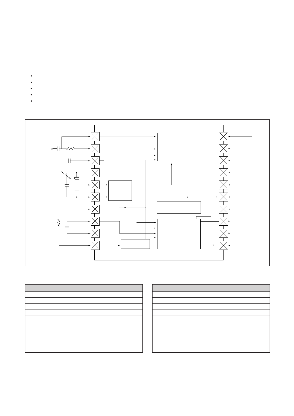
Terminal 21 Pin EURO SCART
2
Page 2
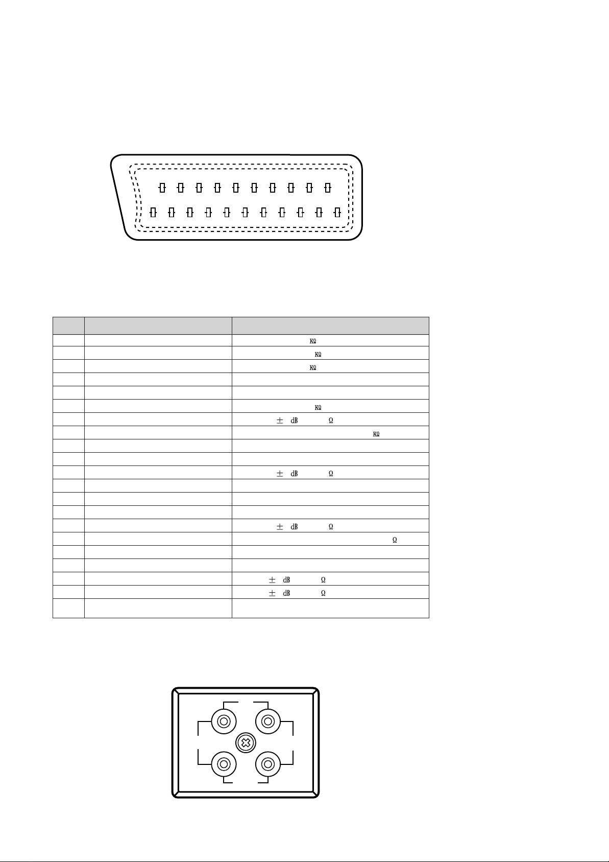
AUX TERMINAL
20 18 16 14 12 10 8 6 4 2
21 19 17 15 13 11 9 7 5 3 1
21 PIN EURO-SCART
PIN Signal Designation Matching Value
1 Audio Out(linked with 3) 0.5Vrms,lmp<1 (RF 60% MOD)
2 Audio In(linked with 6) 0.5Vrms,lmp>10
3 Audio Out(linked with 1) 0.5Vrms,lmp<1 (RF 60% MOD)
4 Audio Earth
5 Blue Earth
6 Audio in (linked with 2) 0.5Vrms,lmp>10
7 Blue in 0.7Vpp 3 ,lmp75
8 Slow(Function) Switching TV:0-2V,PERI:9.5-12V,lmp>10
9 Green Earth
10 NC
11 Green In 0.7Vpp 3 ,lmp75
12 NC
13 Red Earth
14 NC
15 Red In 0.7Vpp 3 ,lmp75
16 Rapid(Blanking) switching Logic 0:0-0.4V,Logic 1:1-3V,Imp 75
17 Video Earth
18 Rapid Blanking Earth
19 Video Out 1Vpp 3 ,lmp75
20 Video In 1Vpp 3 ,lmp75
21 Common Earth
RCA JACK
AUDIO
IN
VIDEO
OUT
3
Page 3

SAFETY INSTRUCTIONS
WARNING: BEFORE SERVICING THIS CHASSIS, READ THE "X-RAY RADIATION
PRECAUTION","SAFETY PRECAUTION" AND "PRODUCT SAFETY NOTICE" BELOW.
X-RAY RADIATION PRECAUTION
1. Excessive high voltage can produce potentially
hazardous X-RAY RADIATION.To avoid such
hazards, the high voltage must not exceed the
specified limit. The nominal value of the high
voltage of this receiver is 25.5 (21":26.5 ) at
max beam current. The high voltage must not,
under any circumstances, exceed 27.5
(21":29.0 ).
Each time a receiver requires servcing, the high
voltage should be checked following the HIGH
SAFETY PRECAUTION
1. Potentials of high voltage are present when this
receiver is operating. Operation of the receiver
outside the cabinet or with the back board
removed involves a shock hazard from the
receiver.
1) Servicing should not be attempted by anyone
who is not thoroughly familiar with the
precautions necessary when working on highvoltage equipment.
2) Always discharge the picture tube before
handling the tube. The picture tube is highly
evacuated and if broken, glass fragments will be
violently expelled.
VOLTAGE CHECK procedure on page 9 of this
manual. It is recommended the reading of the
high voltage be recorded as a part of the service
records, It is important to use an accurate and
reliable high voltage meter.
2. The only source of X-RAY Radiation in this TV
receiver is the picture tube.For continued X-RAY
RADIATION protection,the replacement tube
must be exactly the same type tube as specified
in the parts list.
2. If any Fuse in this TV receiver is blown, replace it
with the FUSE specified in the Replacement
Parts List.
3. When replacing a high wattage resistor(oxide
metal film resistor)in circuit board, keep the
resistor 10mm away from circut board.
4. Keep wires away from high voltage or high
temperature components.
5. This receiver must operate under AC230 volts,
50Hz. NEVER connect to DC supply or any other
power or frequency.
PRODUCT SAFETY NOTICE
Many electrical and mechanical parts in this have
special safety-related characteristics. These
characteristics are often passed unnoticed by a
visual inspection and the X-RAY RADIATION
protection afforded by them cannot necessarily be
obtained by using replacement components rated
for higher voltage,wattage,etc. Replacement parts
which have these special safety characteristics are
identified in this manual and its supplements,
electrical components having such features are
identified by designated symbol on the parts list.
Before replacing any of these components, read the
parts list in this manual carefully. The use of
substitute replacement parts which do not have the
same safety characteristics as specified in the parts
list may create X-RAY Radiation.
5
Page 4
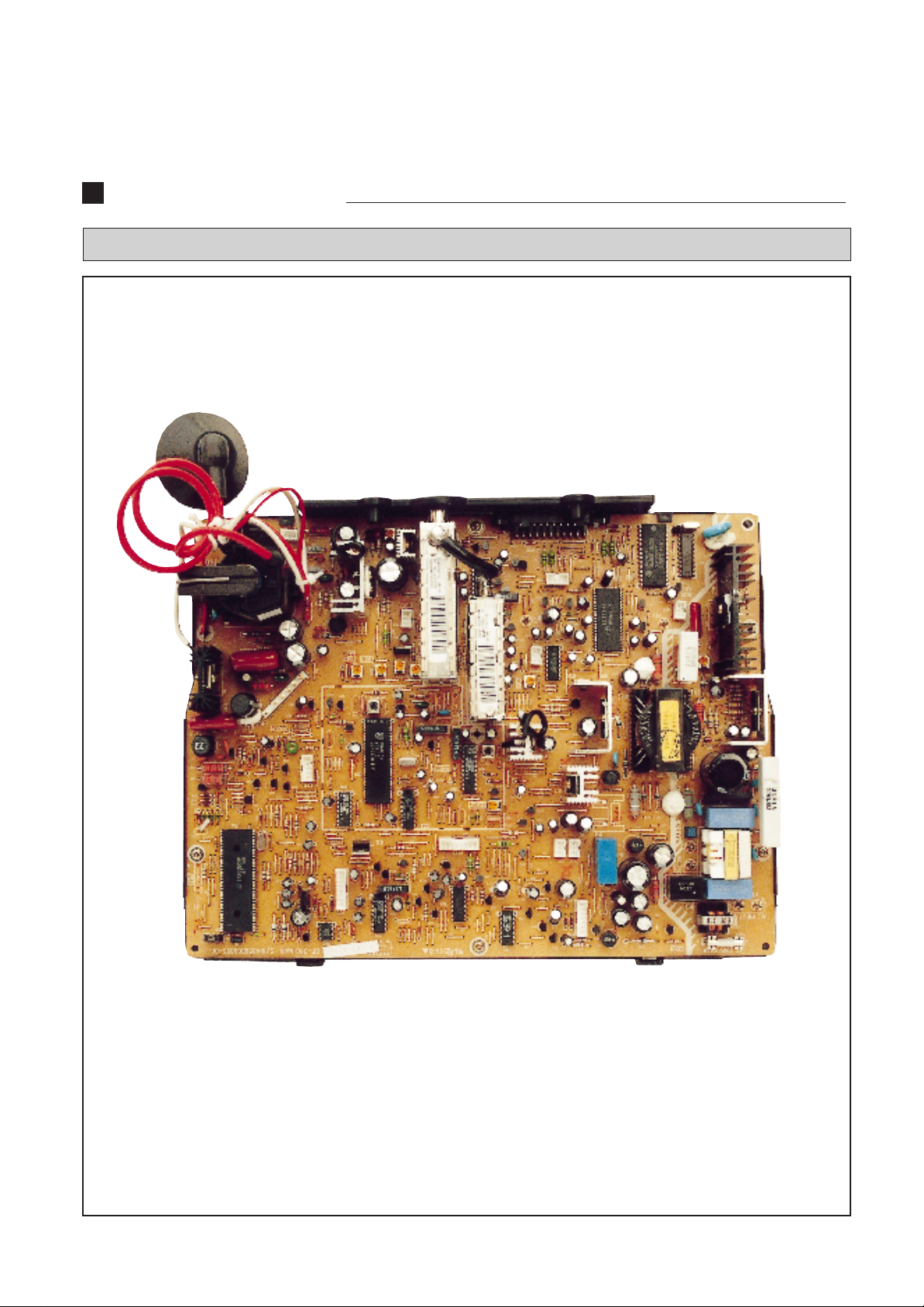
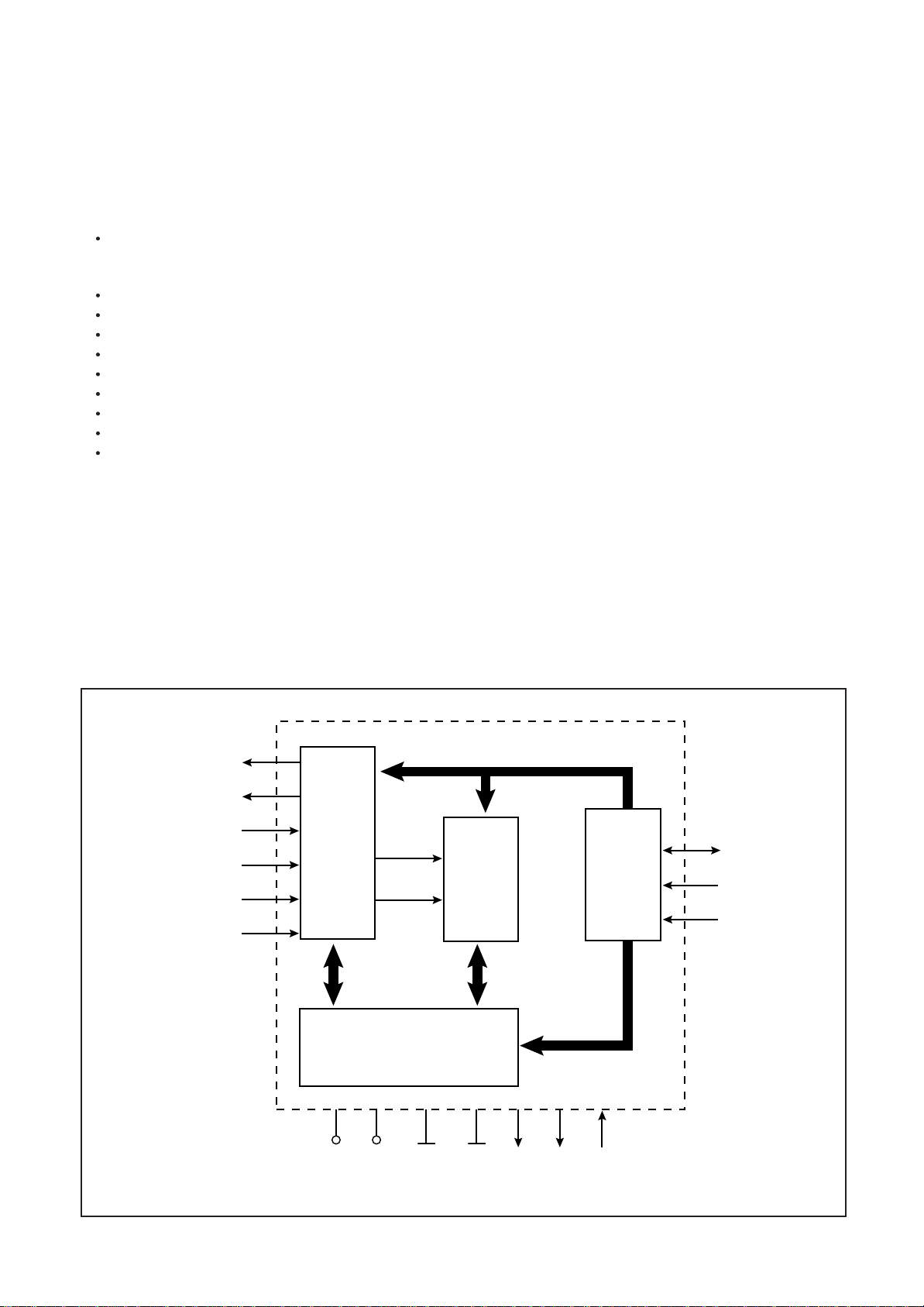
ASSEMBLY VIEW
MAIN BOARD VIEW
6
Page 5

INSTALLATION & SERVICE ADJUSTMENTS
GENERAL INFORMATION
All adjustments are thoroughly checked and
corrected when the receiver leaves the factory.
Therefore the receiver should operate normally
and produce proper colour and B/W pictures upon
installation. But, several minor adjustments may
be required depending on the particular location in
which the receiver is operated. This receiver is
shipped completely in a card-board carton.
Carefully draw out the receiver from the carton
and remove all packing materials.
Plug the power cord into an AC power outlet. Turn
the receiver ON and adjust the FINE TUNING for
the best picture detail. Check and adjust all the
customer controls such as BRIGHTNESS,
CONTRAST and COLOUR Controls to obtain a
natural B/W picture.
PROTECTION CIRCUIT CHECK
1. Turn on the receiver.
2. The receiver must be turned off and changed to
stand-by mode.
HIGH VOLTAGE CHECK
1. Connect an accurate high voltage metre to the
anode of the picture tube.
2. Turn on the receiver. Set the BRIGHTNESS
and CONTRAST controls to minimum(zero
beam current).
3. High voltage should be below 27.5 (21":29.5 )
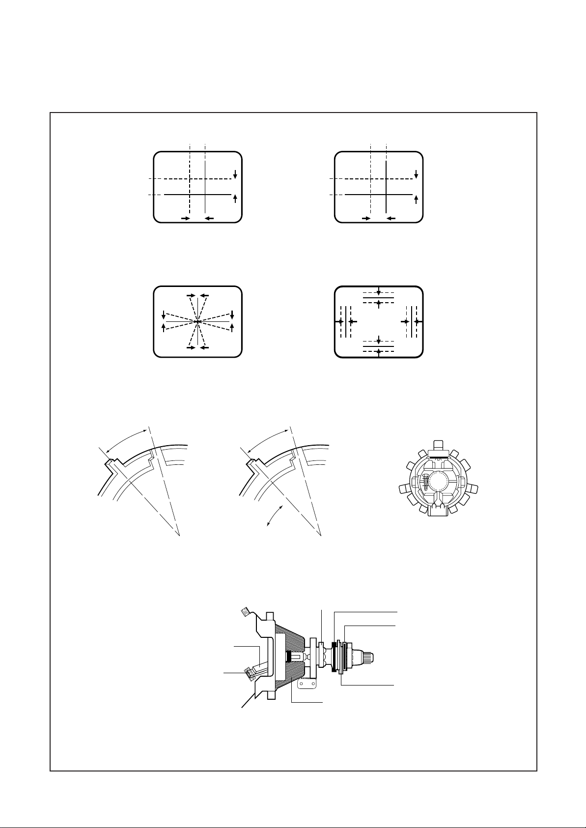
DYNAMIC CONVERGENCE
ADJUSTMENT
Dynamic convergence (convergence of the three
colour field at the edges of the CRT screen)is
accomplished by proper insertion and positioning
of three rubber wedges between the edges of the
deflection yoke and the funnel of the CRT. This is
accomplished as follows:
1. Switch the receiver on allow it to warm up for 15
minutes.
2. Apply crosshatch pattern from dot/bar generator
to the receiver. Observe spacing between lines
around edges of the CRT screen.
3. Tilt the deflection yoke up and down, and insert
tilt adjustment wedges 1 and 2 between the
deflection yoke and the CRT until the misconvergence illustrated in figure. 2(A) has been
corrected.
4. Tilt the deflection yoke right and left, and insert
tilt adjustment wedge 3 between the deflection
yoke and the CRT until mis-convergence
illustrated in figure. 2(B) has been corrected.
5. Alternately change spacing between, and depth
of the insertion of, the three wedges until proper
dynamic convergence is obtained.
6. Use a strong adhesive tape to firmly secure
latch of the three rubber wedges to the funnel of
the CRT.
7. Check purity and readjust, if necessary.
AUTOMATIC DEGAUSSING
A degaussing coil is mounted around the picture
tube so that external degaussing after moving the
receiver is normally unnecessary. Providing the
receiver is properly degaussed upon installation.
The degaussing coil operates for about 1 second
after the power of the receiver is switched ON.If the
set is moved or placed in a different direction, the
power switch must be switched off for at least 15
minutes in order to make the automatic degaussing
circuit operate properly.
Should the chassis or parts of the cabinet become
magnetized to cause poor colour purity,use an
external degaussing coil. Slowly move the
degaussing coil around the faceplate of the picture
tube, the sides and front of the receiver and slowly
withdraw the coil to a distance of about 2m before
disconnecting it from the AC source.
If colour shading still persists, perform the COLOUR
PURITY ADJUSTMENT and CONVERGENCE
ADJUSTMENTS procedures, as mentioned later.
STATIC (CENTRE) CONVERGENCE
ADJUSTMENT
1. Switch the receiver on and allow it to warm up for
15 minutes.
2. Connect the output of a crosshatch generator to
the receiver and concentrating on the centre of the
CRT screen, proceed as follows:
a. Locate the pair of 4 pole magnet rings. Rotate
individual rings (Change spacing between tabs)to
converge the vertical red and blue lines.Rotate the
pair of rings (maintaing spacing between tabs)to
converge the horizontal red and blue lines. (Refer to
fig. 1 (A))
b. After completing red and blue centre
convergence, locate the pair of 6 pole magnet rings.
Rotage individual rings (change spacing between
tabs) to converge the vertical red and blue
(Magenta)and green lines. Rotate the pair of rings
(maintaining spacing between tabs)to converge the
horizontal red and blue(Magenta) and green
lines.(Refer to Fig. 1(B))
8
Page 6
COLOR PURITY ADJUSTMENT
For the best result,it is recommended that the
purity adjustment is made in final receiver
location. If the receiver will be moved, perform
adjustment with it facing east. The receiver must
have been operating 15 minutes prior to this
procedure and the faceplate of the CRT must be
at room temperature. The receiver is equipped
with an automatic degaussing circuit. But, if the
CRT shadow mask has become excessively
magnetized, it may be necessary to degauss it
with manual coil. Do not switch the coil.
The following procedure is recommended while
using a dot generation.
1. Check for correct location of all neck
components (See figure. 5).
2. Rough-in the static convergence at the centre
of the CRT, as explained in the static
convergence procedure.
3. Rotate the picture control to centre of its
rotation range, and rotate brightness control to
max. CW position.
4. Apply green color signal to produce a green
raster.
5. Loosen the deflection yoke tilt adjustment
wedges (3), loosen the deflection yoke clamp
screw and push the deflection yoke as close as
possible to the CRT screen.
6. Begin the following adjustment with the tabs on
the round purity magnet rings set together,
initially move the tabs on the round purity
magnet rings to the side of the CRT neck.
Then, slowly separate the two tabs while at the
same time rotaing them to adjust for a uniform
green vertical band at the CRT screen.
7. Carefully side the deflection yoke backward to
achieve green purity. (uniform green screen)
Centre purity was obtained by adjusting the
tabs on the round purity magnet rings, outer
edge purity was obtained by sliding the
deflection yoke forward.
Tighten the deflection yoke clamp screw.
8. Check for red and blue field purity by applying
red signal and touch up adjustments, if
required.
9. Perform black and white tracking procedure.
SCREEN & WHITE BALANCE
ADJUSTMENT
1. This adjustment is to be made only after
warming up at least 15 minutes.
2. Receive RETMA pattern signal.
3. Set the RGB Bias VR (R522,R512,R502) to
minimum.
4. Set the G,B Drive VR (R515,R505)to center.
5. Set the CONTRAST, BRIGHTNESS, COLOR
control to MIN, and Sub-bright VR(R 13)to
CENTER.
6. Rotate the R, G and B Bias VR of the other
color which did not appear on the screen
clockwise, until a dim white is obtained.
7. Set the CONTRAST, BRIGHTNESS, COLOR
control to MAX.
8. Set the G, B Drive VR to obtain the best white
uniformity on the screen.
9. Rotate the CONTRAST, BRIGHTNESS,
COLOR controls until a dim raster is obtained
and touch-up adjustment of RGB Bias VR to
obtain the best white uniformity on the screen.
SUB-BRIGHTNESS ADJUSTMENT
1. White balance adjustment must proceed this
procedure.
2. Set the CONTRAST, BRIGHTNESS, COLOR
control to MIN.
3. Rotate the SUB-BRIGHTNESS VR (R 13)
gradually CCW until the last beam disappears
on the screen.
VERTICAL HEIGHT ADJUSTMENT
1. Receive RETMA pattern signal.
2. Set the BRIGHTNESS control and CONTRAST
control to Max., and the COLOR control to
centre.
3. Adjust R 11 for the optimum vertical height and
over scanning.
VERTICAL CENTER ADJUSTMENT
1. Receiver RETMA pattern signal.
2. Adjust R 3 so that the vertical center of the
picture may be coincident with the mechanical
center of CRT.
HORIZONT AL CENTER
ADJUSTMENT
1. Receive RETMA pattern signal.
2. Adjust R 12 so that the horizontal center of the
picture may be coincident with the mechanical
center of CRT.
FOCUS VOLTAGE ADJUSTMENT
1. Receive RETMA pattern signal.
2. Adjust the FOCUS VOLUME on the FBT and
make the picture on the screen be finest.
9
Page 7

RF AGC ADJUSTMENT(MAIN)
RF AGC ADJUSTMENT(SUB)
1. Receive PAL COLOR BAR signal in the VHF
high band where the strength of signal can be
75dB.
2. Set the CONTRAST control to Max., the
BRIGHTNESS control to provide adequate black
and gray scales.
3. Connect an oscilloscope to P211.(Tuner AGC
point)
4. Maintain the fine tuning on the screen, and adjust
R010(AGC DELAY CONTROL VR.) to max.
5. Adjust the VR(R010) max to below
2.2V(FA/LA:2.2V).
MAIN B+(+103V) ADJUSTMENT
1. Set the picture level to service 1
mode.(Bright:31, Colour:31, Contrast:48,
Sharpness:48)
2. Connect DC voltage meter to the P805 and
adjust R080 for +103V DC.
1. Receive PAL COLOR BAR signal in the VHF
high band where the strength of signal can be
75dB.
2. Set the CONTRAST control to Max., the
BRIGHTNESS control to provide adequate black
and gray scales.
3. Connect an oscilloscope to P211.(Tuner AGC
point)
4. Maintain the fine tuning on the screen, and adjust
R090(AGC DELAY CONTROL VR.) to max.
5. Adjust the VR(R090) max to below
2.2V(FA/LA:1.6V).
10
Page 8
BLUE
RED
RED/BLUE
GRN
ADJUST THE
ANGLE
(VERTICAL
LINES)
BLUE
RED
RED/BLUE
GRN
(A)
4-Pole Magnets Movement
6-Pole Magnets Movement
FIG. 1 CENTER CONVERGENCE BY CONVERGENCE MAGNETS
B G R
R
G
B
R G B
B
G
R
(A)
Incline the Yoke up (or down)
B
G
R
BGR
Incline the Yoke right (or left)
FIG. 2 CIRCUMFERENCE CONVERGENCE BY DEF .YOKE
CONSTANT
(B)
(B)
R
G
B
BGR
WEDGE1
ROTATE TWO TABS AT
THE SAME TIMER
(HORIZONTAL LINES)
ADJUSTMENT OF MAGNETS
WEDGE2
DEFLECTION YOKE REAR VIEW
WEDGE3
FIG. 3 ADJUSTMENT OF MAGNETS FIG. 4 RUBBER WEDGE LOCATION
DEFLECTION
YOKE CLAMP
RUBBER
WEDGES
TAPE
SCREW
DEFLECTION YOKE
TILT ADJUSTMENT WEDBE
PURITY MAGNETS
6 POLE CONV
MAGNETS
4 POLE CONV
MAGNETS
FIG. 5 PICTURE TUBE NECK COMPONENT
11
Page 9
PIF ADJUSTMENT(MAIN)
1. APPARATUS CONNECTION AND
PRESETTING
CONNECTION
1) Connect H-out of LSW-480 to X-axis of the
oscilloscope and V-out of LSW-480 to Yaxis of the oscilloscope.
2) Connect the sweep signal output to TP1.
3) Set ATTENUATOR of LSW-480 to 10dB.
4) Supply 12V DC voltage(B+) to TP4 and
TP6.
5) Supply 4-5V DC voltage to TP3.
PRESET
1) Oscilloscope Scaling
a) Put the scale of X and Y of the oscilloscope
to DC level.
b) Set the horizontal time display to X-Y.
c) Put the horizontal axis(X) to 1V/div. And the
vertical axis(Y) to 2V/div.
2) LSW-480 MARKER FREQ. SETTING.
Fp(n+1) fs fc fp-2 fp fs(n-1)
B/G,L/L' 31.9 33.4 34.5 36.9 38.9 40.4
I 31.9 33.5 35.07 37.5 39.5 41
(ADJUSTMENT OF L')
T.P
PIF SWEEP MARKER
GENERATOR
(LSW-480,480-U80)
OUTPUT
V-Scope H-Scope
OSCILLOSCOPE
X
Y
Connection For PIF Adjustment
TP5 (Q205 COLLECTOR) GND
TP2 (AFT,I201 #44)
TP1 (U1, IF1)
TP4 (1717 #1) TP6(C727) TF3 (I201 #48)
(B+) (IF AGC)
14V
DC
POWER SUPPLY
2. ADJUSTMENT OF AFT(B/G, I, L)
1) Connect the test point of LSW-480 to TP2.
2) Adjust L201(AFT COIL) so that the P marker
point is located on the reference level.
MAIN PCB
Through a 4.7K resistor
4-5V
DC
POWER SUPPLY
B/G, L : 38.9MHz
I : 39.5MHz
P
3. ADJUSTMENT OF SECAM-L' AFT
1) Connect the TP5 (Q205 collector) to GND.
2) Adjust C200(L'AFT TRIMMER) so that the C
marker point (34.5MHz) is located on the
reference level.
AFT WAVEFORM
L' : 34.5MHz
C
L'AFT WAVEFORM
12
Page 10
PIF ADJUSTMENT(SUB)
1. APPARATUS CONNECTION AND
PRESETTING
CONNECTION
1) Connect RF-out of PM5518 to TP7.
2) Connect DC voltage meter to TP8.
3) Supply 14V DC voltage(B+) to TP4 and TP6.
PM5518
PATTERN
GENERATOR
RF OUTPUT
TP7 (U2, IF1)
TP8 (I901 #15)
PRESET
1) PM5518 SETTING
Freq. (MHz) Remark
B/G,L 38.9 FA/LA
I 39.5 PA
L' 34.5 LA
MAIN PCB
DIGITAL
MULTIMETER
Connection For PIF Adjustment
2. ADJUSTMENT OF AFT(B/G, I, L)
1) Connect the DC voltage meter to TP8.
2) Adjust L902(AFT COIL) for 2.2±0.1V.
TP4 (I717 #1) TP6(C727) TP9 (Q904 BASE)
Through a 22K resistor
(ADJUSTMENT OF L')
14V
DC
POWER SUPPLY
5V
DC
POWER SUPPLY
3. ADJUSTMENT OF SECAM-L' AFT
1) Supply 5V DC voltage to TP9.
2) Connect the DC voltage meter to TP8.
3) Adjust R091(L'AFT VR.) for 2.2±0.1V
13
Page 11
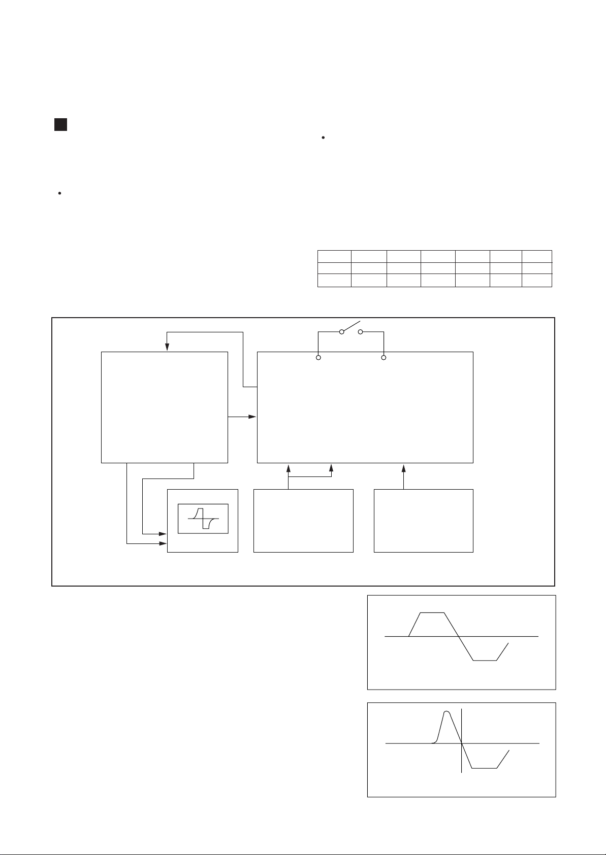
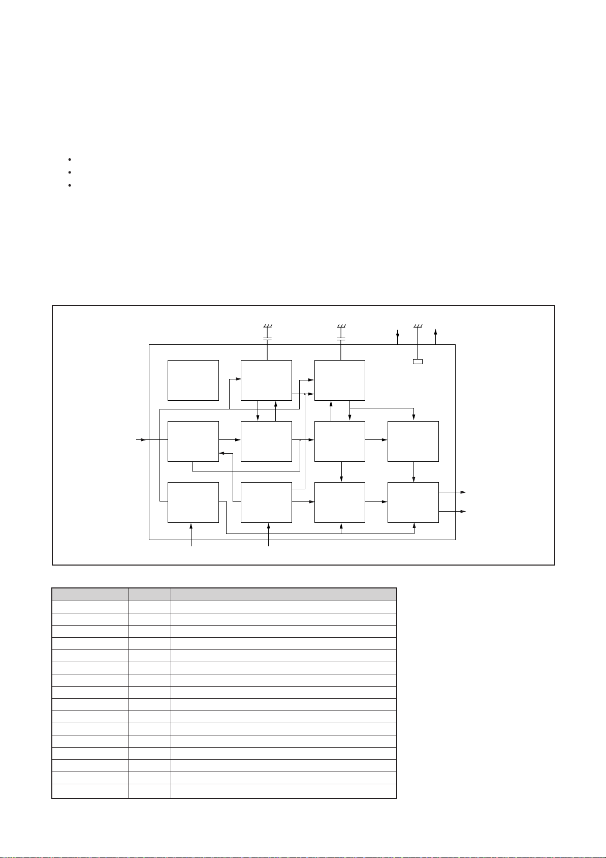
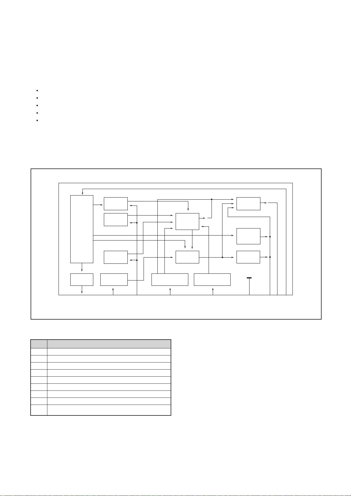
IC OPERATION DESCRIPTION
M37206MC-xxxSP (Micro-controller)
(1) General Description
It is a one-chip micro-controller with an 8-bit CPU.
(2) Functional Block Diagram
OSD OSC
OSD OSC
(PULL UP) PIF MUTE
AFT IN1
P.F IN(L)
AFT IN2
(PULL UP) VOLUMOUT
(PULL UP)CONT. OUT
(PULL UP)BRIGHT OUT
(PULL UP)COLOUR OUT
(PULL UP)PEAKING OUT
(PULL UP)TINT OUT
(PULL UP)L1' OUT
(PULL UP)L2' OUT
TEXT1 USE
TEXT2 LANG
TEXT3 LANG
SYS OSD
SECAML
SYNC1 "H"
(PULL UP) IIC CLK
(PULL UP) IIC DATA
(IDENT) SYNC LOW IN
(PULL UP) SERIAL IN
(PULL UP) SERIAL CLK
(PULL UP) SERIAL OUT
GND
GND
RESET(L)
8.0 MHz
8.0 MHz
GND
1
2
3
4
5
6
7
8
9
10
11
12
13
14
15
16
17
18
19
20
21
22
23
24
25
26
27
28
29
30
31
32
OSC1
OSD2
P MUTE
AFT1
P.F IN
AFT2
VOL. PWM
CONT. PWM
BRI. PWM
COL. PWM
PEA. PWM
TINT. PWM
L1' OUT
L2' OUT
OP.8
OP.9
OP.10
OP.11
OP.12
SYNCI
SCL
SDA
SYNC. L
SD_IN
SD_CLK
SD_OUT
GND
GND
RESET
XIN
XOUT
GND
Vcc
H. SYNC
V. SYNC
BLK
TV 1/2
SYS1
SYS2
V MUTE
S MUTE
TV PWR
DISABLE
A/V1
A/V2'
A/V1'
SCIN
A/V
OP. 7
OP. 6
OP. 5
OP. 4
OP. 3
OP. 2
OP. 1
XCOUT
XCIN
+ 5V
64
H.SYNC INPUT
63
V.SYNC INPUT
62
R
G
B
R OUT
61
GUT
60
B OUT
59
NC
58
BLANKING OUT
57
TV 1/2 SEL OUT
56
STSTEM1 OUT
55
SYSTEM2 OUT
54
53
52
51
V MUTE OUT
50
SPEAKER MUTE
49
TV POWER ON/OFF
48
DISABLE
47
A/V1 SEL OUT
46
A/V2' SEL OUT
45
A/V1' SEL OUT
44
SCART IN (S/SW)
43
A/V SEL OUT
42
VPS/PDC
41
CLK TEST
40
POWER ON START
39
SHOWVIEW
38
AV2
37
U BAND
36
TAPE SPEED
35
32.768 KHz
34
32.768 KHz
33
14
Page 12
(3) Functional Block Diagram
Pin No. Symbol Name Function Description
1 OSC IN Oscillator for OSD OSD (On Screen Display)
2 OSC OUT
3 P MUTE PIF MUTE Not used
4 AFT1 ADC Input
5 P.F INPUT POWER FAIL Input Power fail detect input.
6 AFT2 ADC Input Input AFT signal from SUB TUNER with level
7 VOL Volume Control Output
8 CON Contrast Control Output
9 BRI Brightness Control Output
10 COL Colour Control Output
11 PEA Peaking Control Output
12 TINT Tint Control Output
13 L1' L1' Output(SECAM)
14 L2' L2' Output(SECAM)
15 OP. 8 Text use Option
16 OP. 9 TURKISH Option Not used
17 OP.10 EAST Option Not used
18 OP.11 System OSD Option SECAM Only
19 OP.12 SECAM-L Option
20 SYNC1 Sync Ident Input
21 SCL Clock Pin for IIC(O)
22 SDA Data Pin for IIC(I/O)
23 SYNC L Sync Low Sync low input (Ident) from SUB TUNER
24 SD IN Syscon serial DATA input
25 S CLK Syscon serial CLOCK out
26 SD OUT Syscon serial DATA out
27 GND GND
Comparison voltage input terminal connected to
built-in comparator.
Input AFT signal from MAIN TUNER with level
conversion (0 to Vdd)
The results of the comparison are used when the
auto search and digital AFT works.
conversion ( 0 to Vdd)
Output the pulse width modulated signal in 63 level
in accordance with 6-bit latch data.
Input terminal of image synchronous signal
necessary for auto search and AFT operation.
In the case of the determination of the level signal
synchronization, the signal state ("H" or "L") which
is input at this terminal is determined every 4ms.
"H" ------------ Presence of synchronization
"L" ------------ Absence of synchronization
Pin SCL and SDA are respectively the data and
clock wire or the multi-master two-wire bidirection
IIC-bus control bus.
If a transmission does not succeed the controller
will retry it for up to 5 times. If the bus is occupied
for longer than 1.18 seconds the u-controller will
generate bursts of nine clock pulses with intervals
of 1.18 seconds until bus is free again.
15
Page 13
Pin No. Symbol Name Function Description
28 GND. GND
29 RESET Reset Input
30 OSCI Clock Input for CPU
31 OSCO Clock Output for CPU
32 GND GND
33 XCIN XC IN 32.768KHz input
34 XCOUT XC OUT 32.768KHz output
35 OP. 1 Tape Speed Option SP/LP option
36 OP. 2 UHF only Option
37 OP. 3 AV2 Option
38 OP. 4 ShowView Option
39 OP. 5 Factory Power Option Power-On start
40 OP. 6 Clock Test Option
41 OP. 7 VPS Option
42 A/V A/V Mode Switching Active "L"
43 S/SW Scart Input Slow switch input
44 AV1' AV1' Switching Out TV2, AV1', AV2' (VCR REC. mode)
45 AV2' AV2' Switching Out
This pin is used to reset the u-controller after a
power-on reset. In order to be sure that the ucontroller starts from an initialized state after the
supply voltage is available, a reset signal has to be
applied.
This reset signal has to be low until a stable 4.19V
supply voltage is available.
The OSCI and OSCO are used to control the onchip oscillator of the u-controller.
OSCI is the input terminal and OSCO the output
terminal.
All internal timing of the u-controller (except for the
OSD part) are derived from this oscillator.
The oscillator frequency has to be 8MHz.
AV1' AV2' Function
LHAV1
HLAV2
H H TV2
46 AV1 AV1 Switching Out Active "L"
47 DISABLE Disable Out Switching Regulator ON/OFF output
48 POWER Stand by ON/OFF
Control Output "L" ----------- power OFF
49 S. MUTE Sound Mute Control
50 V. MUTE Video Mute Control Not Connected
51 n.c. Not Connected
52 n.c. Not Connected
53 n.c. Not Connected
54 SYS2 SECAM-L/L' Switch SECAM-L/L' switch(TV2)
55 SYS1 SECAM-L/L' Switch SECAM-L/L' switch(TV1)
The switch-mode power supply is controlled.
"H" ---------- power ON
Mute Output is active "H"
On power on/off state, instantaneously cut off the
sound and video.
16
Page 14

Pin No. Symbol Name Function Description
56 TV1/2
57 BLK Blanking Signal for OSD
58 n.c. Not Connected
59 B OSD Blue Colour Output
60 G OSD Green Colour Output
61 R OSD Red Colour Output
62 V-sync V-sync input for OSD
63 H-sync H-sync input for OSD
64 Vcc Power supply input terminal
TV1 / TV2 selection switch
"H" -------------- TV1
"L" --------------- TV2
Output R,G and B deliver the colour components for
the OSD while output BLK is used as a test
blanking signal.
The output polarity of the R,G,B and BLK terminals
are active "H".
Input terminal for CRT display vertical synchronous
signal.
Input rectangular pulses whose amplitude is in the
range from 0 to 5V.
The signal state should be active for the time more
than that required for three scanning lines.
The input polarity is active "L".
Input terminal for CRT display horizontal
synchronous signal.
Input rectangular pulses whose amplitude is in the
range from 0 to 5V.
The input polarity is active "L".
The signal state should be active for the time more
than that required for three scanning lines.
Connected to the 5V power supply.
17
Page 15
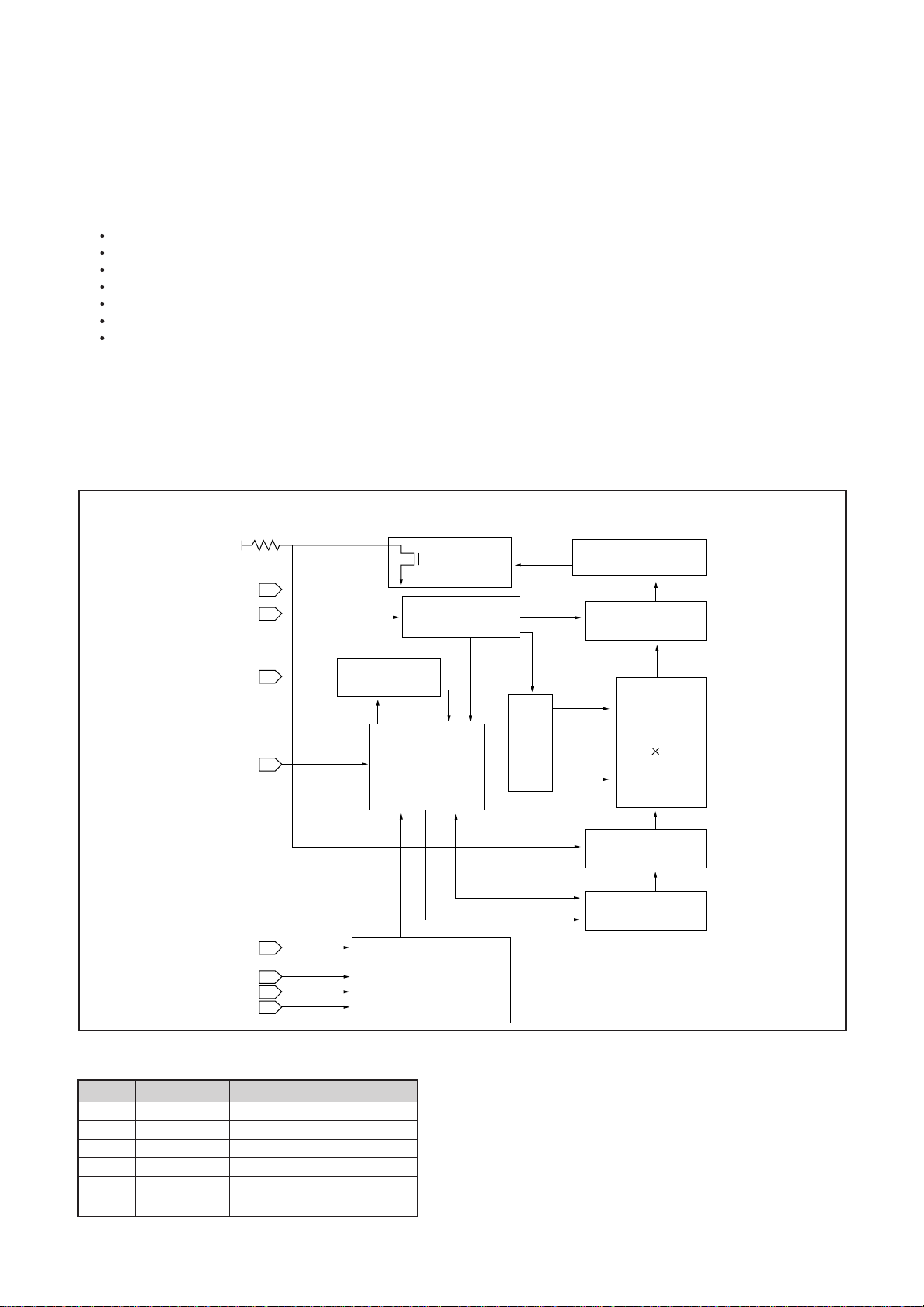
TDA 8362
(1) Features
Multi-standard vision IF circuit (positive and negative modulation)
Multi-standard FM sound demodulator (4.5 MHz to 6.5 MHz)
Video and audio switches (CVBS int/ext, S-VHS and audio int/ext)
Integrated chroma trap and bandpass filters (autocalibrated)
Luminance delay line integrated
PAL/NTSC colour decoder with automatic search system
Easy interfacing with the TDA 8395 (SECAM decoder)for multi-standard applications
RGB-control circuit with linear RGB inputs and fast blanking
Horizontal synchronization with two control loops and alignment-free horizontal oscillator
Vertical count-down circuit and vertical pre-amplifier
Low dissipation(only 600mW)
Small amount of peripheral components compared with competition IC's
Only one adjustment (vision IF demodulator)
(2) Description
Vision IF amplifier, video demodulator, video amplifier, AGC and AFC suitable for both negative and
positive modulation.
Sound limiter,demodulator and amplifier with volume control.
Inputs and switches for external audio and CVBS signals.
Synchronization circuit with drive circuits for horizontal and vertical deflection.
X-ray protection (combined with the 2nd phase detector pin).
PAL/NTSC color decoder in which the chroma filters (bandpass and trap) and the luminance delay line
have been integrated. The circuit has a separate chroma input and the filters can be switched-off so that
S-VHS signals (via an external switch) can be applied to the IC.
For SECAM applications an (alignment-free) SECAM-decoder can be added to the IC.
Peaking circuit in the luminance channel.
RGB-output circuit with linear inputs for On-screen Character Display.
(3) Block Diagram
AUDIO OUT
AUDIO PAE-AMP
+VOL.-CONTR.
T.O.P.
TUNER
IF
AFG
IDENT
AGC FOR IF
+ TUNER
VIF AMPLIFIER
+DEMODULATOR
AFC + S/M VIDEO AMPL
VIDEO
IDENT
AUDIO
IN
AUDIO
SWITCH
SOUND LIMITER
MODULATOR
FILTER TUNING
CVBS
VIDEO SWITCH
CVS
in
SOUND
TRAP
POS/NECC
MCO.
SW
SOUND
BANDP.
SYNC
SEPARATOR
+ 1st LOOP
CHROMA
TRAP
+ DELAY LINE
CHROMA
BANDP.
SWITCH
CONTROL
Chr
+sw.
PEAKING
VOLUME
CONTROL
SHIFT
H. OUT
RGB-INPUT
+SWITCH
RGB-MATRIX
+OUTPUT
PEAK-WHITE
LIMITER
CONTRAST
BRIGHTNESS
+ START
H
+
V
BL
R
G
B
A
G
B
+BV
VCO +
CONTROL
REF
VERT.SYNC
SEPARATOR
LUMINANCE
PROCESSING
Chr
PAL/NTSC
DECODER
Chr
HUE
+ SW.
+ Chr out
SECUMREF.
R.Y B.Y R.Y B.Y
3.6
4.4
2nd LOOP
+ HOR SHIFT
H/V DIVIDER VERT.DEFL.
G+Y MATRIX +
SATURATION
CONTROL
TDA 4661
SATURATION
18
Page 16
Pin No.
1 Audio De-emphasis At this pin the audio signal is available for scart. The signal has an
2,3 IF Because the demodulator performance depends on the Q factor, we
Demodulator
Tuned Circuit
4 Video The identification output has a three level output, 0.5, 6 or 8V.
Identification
Output
Name Function Description
amplitude of 350mVrms (at f= 50KHz) is non volume controlled and
has to be buffered.(notice the output impedance influences the
deemphasis).For scart requirements, the buffer should be dimensioned
as an amplifier in order to increase the output signal. A third function of
this pin is the positive modulation switch. When the voltage at this pin is
above Vcc-1V positive modulation is selected. The current needed is
100 A typical.
want to keep the Q factor as high as possible. But this means that the
steepness of the AFC will change with the Q factor of the tuned clicuit
itself and also with the input impedance of the IC A compromise has to
be made. The input impedance of the IC is as large as possible (about
12 kOhms) and the Q factor of normal tuned circuits varies from 70 to
90. By means of an external resistor, it is possible to damp the circuit to
a Q of 40 to reduce the steepness variation of the AFC.
Output voltage "video not identified" 0.5V max
Output voltage "video identified" 6V
and colour signal available with fsc = 3.5MHz
Output voltage "video identified" 8V
and colour signal available with fsc = 4.4MHz or
no colour signal detected
The maximum load current on this pin is 25 A.
The output impedance is 20 K .
5 SIF input The sound input impedance is 8.5K /5pF which has to be taken into
+Volume control
6 External Audio Input External sound signals from scart, for example, can be applied to this
7 IF Video Output A multistandard concept requires several filters at the video output
8 Decoupling Decoupling Digital Supply
digital Supply
account for the ceramic filiters. For DC, the impedance is very high. The
PLL is sensitive for high freq. AC signal > 1mVrms. Because of the
chosen principle: an adjustment free PLL it is needed to have an
internal PLL with a large bandwidth (catching range). This implies the
system also is sensitive for spurious frequencies. Both layout and
sound band pass filters need special attention. The volume can be
controlled at this pin by means of a DC voltage of 0.2-5V for min-max
gain.
pin via a capacitor. The input impedance is 25 K .
(sound-trap and sound-band pass filters). This causes a too big
capacitive load at the video output so an EMITTER FOLLOWER as
buffer should be added. The required emitter current depends on the
number of filter applied.
9 Ground Ground 1 (IF, H sync, RGB output, Digital, H output)
10 Positive Supply (8V) Supply (IF,Sound,H sync,Chroma, Filters,RGB output, Digital,)
11 Ground Ground 2 (Sound,Chroma,Filters,Hosc, PHI-1, PHI-2)
19
Page 17
Pin No.
12 Decoupling Variations in the tuning voltage outside calibration (i.e. during field
filter tuning
13 Internal CVS input The internal and external CVBS amplitudes should be 2Vpk-pk and
15 External CVS input 1Vpk-pk respectively; their source impedances should be low so as to
14 Peaking control input The input impedance of pin 14 is very high (MOS input). The DC
16 AV switch input The input impedance of the chroma and A/V switch input(pin 16) is 15K
+ Chroma (SVHS) input
Name Function Description
scan), due to external leakage current or interference sources, will
result in mistuning of the luminance notch filter, chroma bandpass filter
and luminance delay stage. Unwanted voltage signals at pin 12 due to
external leakage currents or cros-stalk from interference sources
should be less than 100mV. A capacitor of 100nF requires that external
leakage at pin 12 should be less than 0.5 A.
minimze cross-talk from interference sources. The internal CVBS input
is derived from the IF video output (pin 7) and the external CVBS input
can be derived from either SCART CVBS or YSVHS; they should be
AC coupled to pins 13 & 15 respectively. The coupling capacitors are
chosen in order to have fast clamping and minimum line/field sag.
voltage at the peaking control input controls the gain of the peaking
amplifier. The peaking control input voltage should have a DC voltage
range from 0 to 5V.
in parallel with 5pF. A DC voltage on this pin controls the internal/
external CVBS and AUDIO selection where the following table gives
the various possibilities:
Vpin 16 Internal External CSVHS Luminance Audio Model
(dc) CVBS CVBS/Y signal notch signal
<0.5V on off off on Internal TV
Between
3V &5V
>7.5V off
off on(Y) on off External S VHS
on
(CVBS)
off on External AV
17 Brightness Control input The brightness control voltage present at pin 17 controls the dc level of
the RGB outputs where a brightness control voltage of 0 5V at pin 17
results in a black level shift at the RGB outputs of 1V about the
nominal.
18 B-output The RGB output signals are supplied to the video output stages. For nominal
19 G-output input signals (i.e. CVBS and -(R-Y)/-(B-/Y) signals) and for nominal gain
20 R-output settings then the RGB output signal amplitudes (black-to-white)are
typically 4V with a black level at approximately 1.3V. The blanking level
is 0.8V and maximum peak white level is 6.0V Since the RGB output
stages are made with emitter followers, the maximum sink current is
limited to 1.5mA. Therefore the current delivered from the video output
stages to the RGB pins must not exceed 1.5mA.When the RGB switch
control (pin 21) voltage exceeds 4V then the RGB outputs are blanked
and consequently on-screen display signals (OSD) can be supplied to
the video output stages.
21 RGB insertion The RGB insertion signals are selected by means of a fast switch
22 R-input for insertion The RGB insertion signal information is coupled via 100nF to pins 22,
23 G-input for insertion 23 and 24 respectively. The coupling/clamping capacitors should always
24 B-input for insertion have a low impedance path to ground for proper clamping operation.
+ Blanking input
control.With the conditions that:0.8V<Vpin21<3.1V then the RGB insertion
signals are selected. And input voltage to blank the RGB- outputs so that
OSD signals can be applied to these outputs is 4.5V (min).
20
Page 18
Pin No.
25 Contrast Control input The contrast control input of 0 5V at pin 25 gives a 20dB gain range
26
27 Chroma output If the Vpin27>6V, the ASM does not search for NTSC signals and the
28 B-Y input The -(R-Y)/-(B-Y) signals, present at pins 11 and 12 of the TDA4661, are
29 R-Y input coupled via 100nF (these capacitors are also clamping capacitors) to
30 R-Y output
31 B-Y output signals are identified. For SECAM signals the output impedance is very
32 4.43 MHz output A SECAM reference signal (4.43 MHz only ) is delivered directly from
33 Loop Fitter One of the important aspects of the PLL is the loop filter connected to
Name Function Description
at the RGB outputs. When one of the RGB output signals exceed 6V, it
is then clipped to 6V and also the gain of the RGB output amplifiers can
be reduced by adapting the contrast voltage using the peak white
limiter (PWL) current, The PWL current during PWL operation is 100 A.
Saturation Control Input
+ Hue Control Input
for TDA8395
(Burst Phase
Detector)
The saturation control input voltage, present at pin 26, is 0 5V. this
corresponds to a 52dB gain range of the -(R-Y)/-(B-Y) signals.
decoder application can only be PAL or PAL/SECAM. The output
impedance with an external resistance of 22K to 8V is then
approximately 500 .The hue control input pin should be provided with
a voltage of 0 to 5V for NTSC decoder applications; within this voltage
range the input impedance is very high (MOS input).
pins 29 and 28. The maximum input current of both pins is 1 A. With
100nF coupling capacitors the voltage drop over a line period is less
than 0.5mV Since the output impedance of pin 11 and 12 of the TDA
4661 is maximal 400 then the signal tracks between the TDA 4661
and the TDA8362 should have good ground shielding and be as short
as possible.
The output impedance of pins 30 & 31 is approximately 250 when PAL/NTSC
high (output switch is open) and any external circuity is not loaded (i.e.
the demodulator output of the TDA 8395). During the line/field blanking
periods of the sandcastle pulse, the demodulator outputs are set to the
correct dc levels so as no offsets exist. The-(R-Y)/-(B-Y) outputs are
coupled, via 1nF, to pins 16 & 14 of the TDA4661 respectively.
pin 32 of the TDA8362 to pin 1 of the TDA8395. When SECAM
siganals are identified by the TDA8395, it withdraws a current of 150 A
from pin 32.The SECAM interface communicates the ident information
via this current to the ASM. If PAL/NTSC signals are not already
identified by the ASM and the identified signal is 50 Hz then an
acknowledge will be given by ASM to the TDA8395 by setting the
voltage at pin 32 to 5V. With SECAM identified, the SECAM reference
signal signal is gated and present at pin 32 only during the field retrace
period. When PAL/NTSC is identified, the output level is 1.5V.
pin 33. It ensures that the PLL synchronizes the VCXO, in both
frequency and phase, with the incoming burst (average burst for PAL
standards). It also determines the dynamic performance of the loop
where the important parameters are: -Noise immunity - Transient
response -Acquisition behaviour The remaining aspects of the
PLL/VCXO are static phase error and X-tal type used at pins 34 or 35.
For small static phase errors (less than 5 the requirements are: -The
combined buest phase detector and VCXO sensitivity are high. The
offset of the burst phase detector output is small. -The external leakage
current at pin 33 is small. The TDA8362 determines the first two; the
third is determined by the external leakage resistance of pin 33 to
ground. Deviations in the VCXO free running frequency due to X-tal or
X-tal load capacitance spreads have negligible influence on the static
phase error because the combined phase detector and VCXO
sensitivity is high. The static phase error is due to the internal offset of
the phase detector output and the external leakge current at pin 33.
Static phase errors much less than 5 were measured.
21
Page 19
Pin No.
34 3.58MHz X-TAL To ensure correct operation of both colour processing and
35 4.43MHz X-TAL connected to pin 34 and 3.58
36 Start Horizontal The minimum current required for the start function is 6.5mA,
37 Horizontal Output This open collector output drives the horizontal output stage. The
Name Function Description
Connection sync calibrationcircuits in the TDA8362, 4.43 X-tals must not be
Connection X-tals must not be connected to pin 35.
Oscilator then the voltage will be approx. >7.2V. The voltage at pin 36 may not
exceed 8.8V, so depending on the application external clamping is
necessary. If the start voltage is below approximately 5.8V then the
horizontal output will be disabled. The decoupling should be sufficent
because the start pin supplies the circuitries needed for the horizontal
output. (The oscillator references, however, are supplied by the
bandgap.) This pin must be connected directly to the supply pin when
no start function is used.
maximum allowable current is 10mA. The saturation voltage then will be
0.3V.
38 Flyback input
+Sandcastle Output Burst typ 5.3V, the output impedance is approx. 1k
39 -2 loop Filter The phase error on screen due to storage time variations depends on
+X-Ray Protection the PHI-2 loopgain. In principle this figure is fixed but will decrease
40 -1 loop Filter The PHI-1 behaviour depends on both the loop filter externally
41 Vertical Feedback The feedback signal is derived by sensing the deflection coil current by
Input means of a resistor. The feedback signal is related to the vertical ramp
42 Vertical Ramp The vertical ramp is defined as: -DC clamping voltage of 2V -AC
Generator amplitude of 1.5Vpp for a 50Hz field signal -AC amplitude of 1.25Vpp
A sandcastle signal is available at this pin for external use. The signal levels are:
Flyback typ 3 V, impedance defined by the flyback circuit.
Field blanking typ 2 V, the output impedance is approx. 4k
The flyback input signal is used for the PHI-2 loop and RGB line
blanking. Pin 38 requires a current of only a few in order to reach
the 3V flyback clamping level. Detection of the flyback pulse (and thus
RGB blanking) only occurs when the input current is at least 100 A.
(The maximum allowable current is 300 A.) Additonal remarks: -Due to
an internal base current at pin 38, the voltage level becomes 3V when
the pin is not loaded. -During start-up pin 38 is forced low by 2mA.
when an additional resistor comes in parallel to the capacitor at pin 39.
The time constant is defined by the external capacitor. The voltage to
switch on the X-ray protection is 6V. (min.)
connected at pin 40 and the PHI-1 output currents. The PHI-1 output
current has been made switchable during scan (a fixed current ratio) in
order to avoid the need of switching the loop filter for normal-and noisysignals. This implies the loop filter can be optimised for both VCR-and
noisy-signals.
signal. The ramp amplitude should be 1Vpp while the DC level is 2.5V
typical. The guard levels are 1 and 4Vtyp. In order to filter horizonatal
into a capacitor is mounted at the input.
for a 60Hz field signal The AC amplitude of 1.5V is important for optimal
pre-correction and 50/60Hz gain correction.
22
Page 20

Pin No.
43 Vertical Output. The vertical drive output is fed to the deflection-IC. The available output
44 AFC Output The AFC steepness can be influenced by the Q of the tuned circuit and
45,46 IF Input DC coupling is allowed, so no series capacitors are necessary. The
47 Tuner AGC Output The tuner AGC is an open collector output which is acting as a variable
48 AGC Increasing of the AGC time constant is achieved by increasing the AGC
49 Tuner Take-Over The control range at this pin is 0.5-4.5V.
Name Function Description
current is minimal 1mA, and the available output voltage is 4-5V. During
retrace the drive output has to be constant and equal to the low level of
0.3V.
output resistors at the AFC output pin (60k output impedance
intermally). Due to current reserve the steepness can be reduced by a
factor 4-5 while the output voltage swing remains 6V. Some small video
information can still be present at the AFC output pin although a S&H
function is applied. This video information can be filtered by an external
capacitor at this pin. The AFC output voltage changes from
approximately 0.5-6.3V. The output impedance of AFC circuit is 50k .
circuit matches the required load impedance for commonly used SAW
filters(2k/3pF).
current source to ground. Normally the output application circuit is
designed for an output current swing of 1-2mA. In order to improve the
dynamical behaviour during channel switching it is possible to sink with
a current of approximately 12mA maximal. The max voltage is Vcc+1V.
Decoupling Capacitor capacitor on pin 48. Increasing this capacitor also results in an
improvement in the catching and holding range of the ident circuit.
Adjustment
Characteristics:
The tuner take
over adjust voltage versus IF input signal is a linear function with a
slope of approximately 20mV/dB. (Measured at an AGC output current
of 1mA) In order to achieve a stable AGC control at strong signals a
decoupling capacitor of at least 1nF at this pin is required.
Alignment:
With the potentiometer connected to pin 49 of the TDA8362, the tuner
take over point can be adjusted when an RF signal is applied to the
aerial input of the tuner.
50 Audio Input The DC output voltage is 3.3V. The volume controlled output signal is AC
coupled to the sound output amplifier. The output impedance is 250 .
51 Decoupling This pin defines the DC voltage at the deemphasis and sound output.
Sound Demodulator The pin forms a low pass filter in the DC feedback loop. This implies
that the sound amplitude for lower frequencies, < fk, is attenuated. A
bigger capacitor, in order to decrease fk, is allowed but increases the
DC setting time.
52 Decoupling Decoupling Bandgap Supply
Bandgap Supply
23
Page 21
TDA4661(Base Band Delay Line)
(1) Features
• Two comb filters, using the switched-capacitor technique,for one line delay time (64µs)
• Adjustment free application
• No crosstalk between SECAM colour carriers
• Handles negative or positive colour-difference input signals
• Clamping of AC-coupled input signals(±(R-Y)and±(B-Y))
• VCO without external components
• 3MHz internal clock signal derived from a 6MHz VCO, line-locked by the sandcastle pulse (64µs line)
• Sample-and -hold circuits and low-pass filters to suppress the 3 MHz clock signal
• Addition of delayed and non-delayed output signals
• Output buffer amplifiers
• Comb filtering functions for NTSC colour-difference signals to suppress cross-colour
(2) General Description
The TDA4661 is an integrated baseband delay line circuit with one line delay. It is suitable for decoders with
colour-difference signal outputs±(R-Y)and±(B-Y).
(3)Block Diagram
16
14
0
5
SIGNAL
CLAMPING
SIGNAL
CLAMPING
analog supply
SANDCASTLE
DETECTOR
10
GND1
pre-amplifiers
FREQUENCY
PHASE
DETECTON
LINE
MEMORY
LINE
MEMORY
DIVIDER
BY 192
digital supply
3
output
buffers
2
6
13
15
4,8
11
colour-difference
output signals
12
n.c.
n.c.
n.c.
n.c.
7
I.c.
(R-Y)
(B-Y)
SAMPLE-
ANDHOLD
SAMPLE-
AND-
HOLD
3 MHz shifting clock
LP
6MHz
VCO
1
V
P2
LP
LP
TDA4661
DIVIDER
BY 2
addition
stages
GND2
(R-Y)
colour-difference
input signals
(B-Y)
V
P1
sandcastle
pulse input
(4)Pin Description
SYMBOL PIN DESCRIPTION
Vp2 1 +5V supply voltage for digital part
n.c. 2 not connected
GND2 3 ground for digital part (0V)
i.c. 4 internally connected
SAND 5 sandcastle pulse input
n.c. 6 not connected
i.c. 7 internally connected
i.c. 8 internally connected
SYMBOL PIN DESCRIPTION
Vp1 9 +5V supply voltage for analog part
GND1 10 ground for analog part (0V)
V0 (R-Y) 11 ± (R-Y) output signal
V0 (B-Y) 12 ± (B-Y) output signal
n.c. 13 not connected
V1 (B-Y) 14 ± (B-Y) input signal
n.c. 15 not connected
1 (R-Y) 16 ± (R-Y) input signal
V
24
Page 22
TDA8395 (Secam Decoder)
(1) Features
Fully integrated filters
Alignment free
For use with baseband delay
(2) Description
The TDA8395 is a self-calibrating,fully integrated SECAM decoder. The IC should preferably be used in conjunction
with the PAL/NTSC decoder TDA8362 and with the switch capacitor baseband delay circuit TDA4661. The IC
incorporates HF and LF filters, a demodulator and an identification circuit (Iuminance is not processed in this IC).
A highly stable reference frequency is required for calibration and a two-level sandcastle pulse for blanking and burst
gating.
(3) Block Diagram
ref PLLref GND
CLOCHE
100 nF
77362
220 nF
V
TEST
p
BANDGAP TUNING TUNING
CVBS
16
ACC
INTERFACE
115
f
ref/IDENT
CLOCHE
FILTER
CONTROL
SAND
PLL
IDENT-
IFICATION
(4) Pin Description
SYMBOL PIN DESCRIPTION
fp1/IDENT 1 reference frequency input/identification input
TEST 2 test output
Vp 3 positive supply voltage
n.c. 4 not connected
n.c. 5 not connected
GND 6 ground
CLOCHEref 7 Cloche reference filter
PLL ref 8 PLL reference
-(R-Y) 9 -(R-Y) output
-(B-Y) 10 -(B-Y) output
n.c. 11 not connected
n.c. 12 not connected
n.c. 13 not connected
n.c. 14 not connected
SAND 15 sandcastle pulse input
CVBS 16 video (chrominance) input
TDA8395
DE-
EMPHASIS
OUTPUT
STAGE
–(R-Y)
9
10
–(B-Y)
25
Page 23
AT24C08PC (EEPROM)
(1)Features
IC Bus compatible
Low power CMOS Technology
16 Byte page write Buffer
Self-Timed write cycle with Auto-Clear
100,000 program/Erase cycles
100 Year Data Retention
Optional High Endurance Device Available
(2)General Description
The AT24C08PC is a 8K bit serial CMOS E2PROM internally organized as 1024x8bits. Catalyst's advanced
CMOS technology substantially reduces device power requirements. The AT24C08PC features a 16 byte
page write buffer.
(3) Block Diagram
EXTERNAL
Vcc
Vgg
SDA
TEST
SEL
A0
A1
A3
WORD ADDRESS
BUFFERS
START/STOP
LOGIC
CONTROL
LOGIC
STATE COUNTERS
SLAVE
ADDRESS
COMPARATORS
D OUT
AKC
XDEC
SENSE AMPS
SHIFT REGISTERS
COLUMN
DECODERS
2
64
E PROM
128
64
DATE IN STORAGE
HIGH VOLTAGE/
TIMING CONTROL
(4) Pin Description
PIN SYMBOL DESCRIPTION
1-3 A0,A1,A2 Device Address Inputs
4 Vss Ground
5 SDA Serial Data/Address
6 SCL Serial Clock
7 TEST Connect to Vss
8 Vcc +5V Power supply
26
Page 24
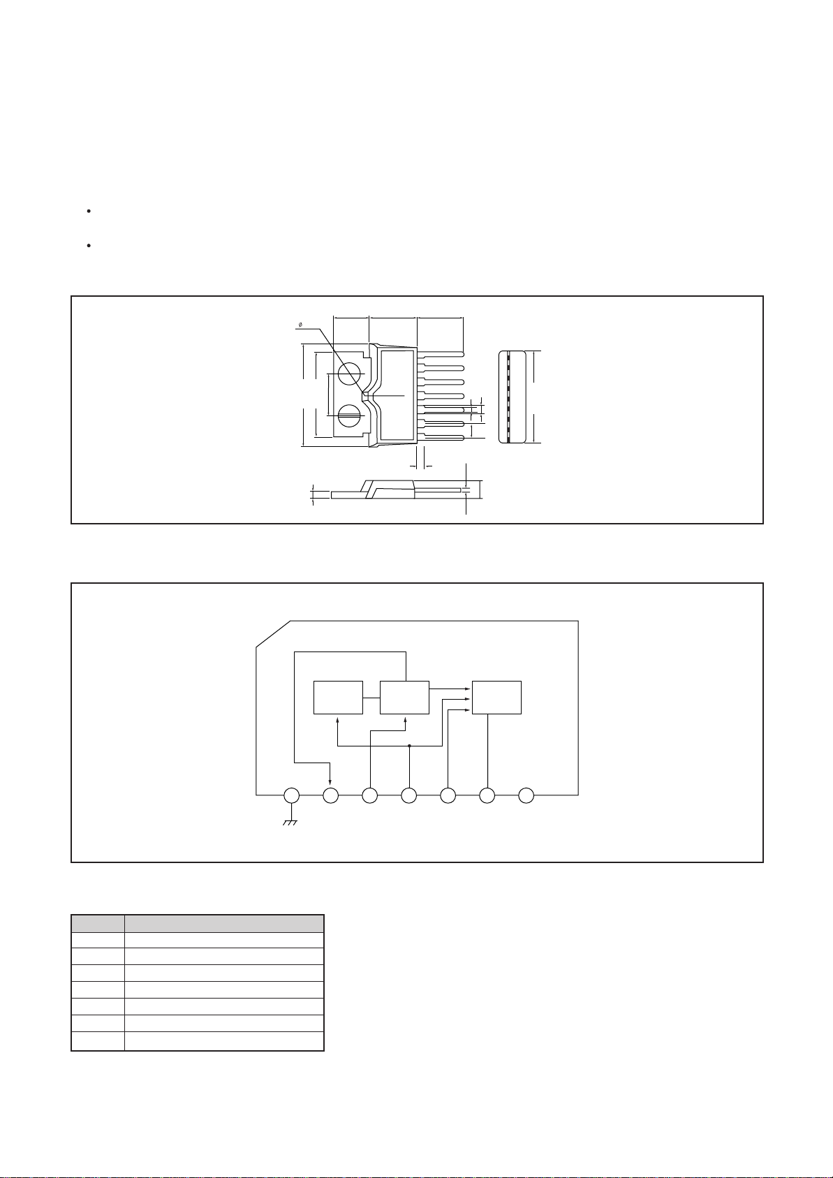
AN5515 (TV Vertical Defelection Output Circuit)
(1)Features
Low power consumption, direct deflection coil driving capability (Flyback voltage two times as high as
supply voltage is supplied during flyback period only)
High breakdown voltage: 50V
(2)General Description
(3)Block Diagram
5.9±0.25
3.6
8.2±0.3
7.8±0.25
7
6
5
1.8R
7.6±6.2
15.3±0.3
17.7±0.3
4
3
0.6±0.1
16.9±0.3
1.4
2
2.54
1.45
3.5±0.3
1.8
Pulse
Amp.
1.2±0.1
Driver
1
1.2
Output
(4)Pin Description
PIN DESCRIPTION
1 GND
2 Output
3 Supply Voltage for Output
4 Input
5 Trigger Pulse Input
6 Pulse Amp. Output
7 Vcc
1 2 3 4 5 6 7
27
Page 25
CF70200 (Teletext Decoder)
(1) Features
Eight pages of on-chip Display RAM
Europe-wide solution
Automatic FLOF & TOP decoding
Flicker-free packet 26 processing on chip
Program delivery control
Minimum software requirement
Menu page capability
Instantaneous page memory clear
75Ω RGB outputs
Digital PLL
Upgrade path from UNITEXT
(2) Block Diagram
SYNC
VIDEO
CSB
SYNC
SWITCH
PLL
RAM
REF
75Ω
DRIVER
RGBSET
R
G
B
RTSK
PROCESSOR
TDATA
TCLK
TELETEXT
FRONT END
PIN PIN NAME DESCRIPTION
1 TEST5 Test Pin
2 SYNC
The output of an internal sync
switch
3 CVBS Video input to sync switch
4 DVcc +5V
5 RSTB System reset active low
6 CLKIN System clock 13.875MHz
7 DGND Ground
8 T1 Test Pin
9 T4 Test Pin
10 TDATA Teletext Data
11 TCLK Teletext Clock Signal
12 CSB Composite Sync Signal
13 MUTE Mute
14 T2 Test Pin
VDP
IC
INTER FACE
BLANK
SDA
SCL
PIN PIN NAME DESCRIPTION
15 WIND WIND
16 T3 Test Pin
17 SCL I2C Clock Line
18 SDA I2C Data Line
19 BLK Blanking
20 B Display Data
21 AVcc +5V
22 G Display Data
23 R Display Data
24 AGND Ground
25 RGBSET
Adjustment for theRGB,Blank
levels
26 REF Internal Reference Pin
27 FLAG1 System Information
28 FLAG2 System Information
28
Page 26
CF72306
(1) Features
Forms a custom 2-chip solution when used with an ASICTEXT decoder
Low power 1um CMOS
Standard 20 pin/300mH package
Tolerates a range of video distortions
Operates with 13.875MHz fundamental mode crystal
(2) Block Diagram
10pF
220pF
13.87MHz
15pF
1 SIG
SSIG
CSIG
AGND 1
15pF
AVGC
220pF
AGND 2
BIAS
OSC 1
OSC 1
CREF
V
BIAS
OSC
13.875MHz
BIAS
I BIAS
ADAPTIVE
SYNC
SEPARATOR
FREOUENCY
MULTIPLER
69MHz
SLICER
DISADLE
DATA
CLK
SCANOUT
SYNC
DGND 1
WIND
DVCC
OSCOUT
SCANOUT
DGND 2
TCLK
TSTAPLB
(3) Pin Description
PIN SIGNAL DESCRIPTION
1 TSIG Video Sync Input 1
2 SSIG Video Sync Input 2
3 CSIG Video Data Input
4 AGND1 Analogue Ground
5 OSC1 13.875MHz Oscillator
6 OSC2 13.875MHz Oscillator
7 AVCC Analogue Vcc
8 CREF Video Data Reference Input
9 AGND2 Analogue Ground
10 BIAS Internal Reference
PIN SIGNAL DESCRIPTION
11 TSTAPLB Test/Application
12 TCLK Teletext Clock
13 TDATA Teletext Data
14 DGND2 Digital Ground
15 OSCOUT Oscillator Output
16 DVCC Digital Vcc
17 WIND Timing Signal
18 DGND1 Digital Ground
19 SYNC Separated Sync Output
20 SCANOUT Test Scan Output
29
Page 27
SDA5648 (VPS/PDC Decoder)
(1) Features
Single-chip receiver for PDC data, broadcast either
- in Broadcast Data Service Packet (BDSP) 8/30/2 according to CCIR teletext system B, or
- in dedicated line no. 16 of the vertical blanking interval(VPS)
Reception of Unified Data and Time (UDT) broadcast in BDSP 8/30/1
Low external components count
On-chip data and sync slicer
IIC-Bus interface for communication with external micro-controller
Selection of PDC/VPS operating mode software controlled by IIC-Bus register
Pin and software compatible to VPS Decoder SDA5642
Supply voltage : 5 V ±10 %
Video input signal level : 0.7 Vpp to 1.4 Vpp
Operating temperature range : 0 to 70°C
(2) General Description
The CMOS circuit SDA 5648 is intended for use in video cassette recorders to retrieve control data of the
PDC system from the data lines broadcast during the vertical blanking interval of a standard video signal.
The SDA 5648 is devised to handle PDC data transported either in Broadcast Data Service Packet(BDSP)
8/30 format 2 (bytes no. 13 through 25) of CCIR teletext system B or in the dedicated data line no. 16 in the
case of VPS.
Furthermore it is able to receive the Unified Date and Time (UDT) information transmitted in bytes no. 5
through 21 of packet 8/30 format 1.
Operating mode (PDC/VPS) is selected by a control register which can be written to via the IIC-Bus interface.
(3) Block Diagram
PD2/VCO 2
I
VCO 1
CVBS
PD1
REF
VCS
DATA-
SyncSlicer
Clock-PLL
Timing
Data-
Acquisition
2
I C Businterface
SDA
SCL
CSO
DD AVDD VSS A VSS D
V
30
DAVN EHB
TI
Page 28
(4) Pin Description
PIN SYMBOL DESCRIPTION
1 Vss GND
2 SCL Serial Clock input of I2C-Bus
3 SDA Serial Clock input of I2C-Bus
4 CS0 Chip select
20H/21H, when pulled low
22H/23H , when pulled high
5 VCS Video Composite Sync output
6 DAVN VPS/PDC data recognition
7 EHB Identification signal for first half
frame
PIN SYMBOL DESCRIPTION
8 TI Test Input
9 PD1 Phase detector/charge pump
output
10 PD2/ Connector of the Loop filter for
VCO2 the SYSPLL
11 VCO1 Oscillator control input
12 IREF Reference current
13 CVBS CVBS input
14 V
DD
Supply voltage (+ 5 V nom.)
31
Page 29
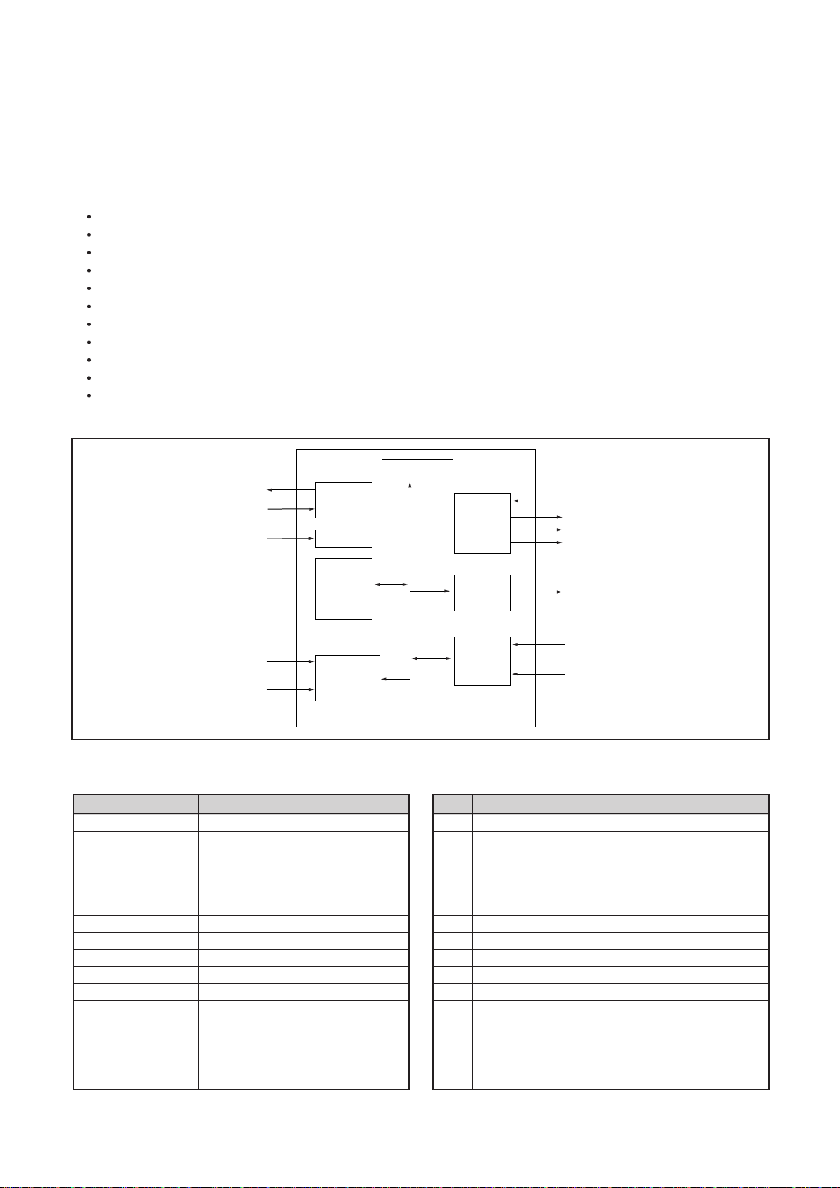
TDA 4601(SMPS Controller)
(1) Features
Direct control of the switching transistor
Low start-up current
Reversing linear overload characteristic
Base current drive proportional to collector current
Protective circuit in case of disturbance
(2) General Description
The integrated circuit TDA4601 is designed for driving, controlling and protecting the switching transistor in
self-oscillation flyback converter power supplies as well as for protecting the overall power supply unit.
(3) Block Diagram
Start-Up
Circuit
Voltage
Control
Reference
Voltage
1 2 3 4 5 6 7 8
Control
Amplifier
Standby
Operation
Overload
Identification
Zero Passage
Identification
(4) Pin Description
PIN DESCRIPTION
1VREF output
2 Zero passage identification
3 Input control amplifier,overload amplifier
4 Collector current simulation
5 Connection for additional protective circuit
6 Ground
7 DC output for charging coupling capacitor
8 Pulse output-driving of switching transistor
9 Supply voltage
Trigger
Start
Hold
Control
Logic
Collector Current
Simulation
Ext. Trigger
Blocking Function
Base Current
Amplifier
Coupling-c
Charging
Circurt
Base Current
Switch-Off
9
32
Page 30

TDA9800 (VIF-PLL demodulator and FM-PLL detector)
(1) Features
Suitable for negative vision modulation
Gain controlled 3-stage IF amplifier; suitable for VIF frequencies up to 60 MHz
True synchronous demodulation with active carrier regeneration (ultra-linear demodulation, good
intermodulation figures, reduced harmonics and excellent pulse response)
Peak sync AGC
Video amplifier to match sound trap and sound filter
AGC output voltage for pnp tuner; adjustable take over point (TOP)
AFC detector without extra reference circuit
Alignment-free FM-PLL detector with high linearity
Stabilizer circuit for ripple rejection and to achieve constant output signals
(2) General Description
Monolithic integrated circuit for vision and sound IF signal processing in TV and VTR sets.
(3) Block Diagram
VP - 5V
IF input
I PC
V
phase
adjust
18
1
2
4
take over
point
20
INTERNAL
REFERENCE
VOLTAGE
3-stage
IF amplifier
TUNER
AGC
3
tuner AGC
output
PLL 2f PC
T
17
3.6V
TRAVELLING
WAVE
DIVIDER
FREQUENCY
DETECTOR
AND PHASE
DETECTOR
6
DEMODULATOR
16
VCO AFC
VIDEO
TDA9800
IF
AGC
12 19 5 8 13 14 11
C
AGC
AGC
DETECTOR
sound MUTE
AFC
VIDEO
AMPLIFIER
n.c.
15
sound
mute
BUFFER AND
NOISE
CLIPPING
SOUND
TRAP
1 V (P-P)
AF
AMPLIFIER
FM.PLL
SOUND
FILLTER
9 V
10
7
O AF
+
C AF
CVBS
2 V (P-P)
FIG.1 Block diagram.
33
MEH191-1
Page 31

(4) Pin Description
PIN SYMBOL DESCRIPTION
1Vi IFa Vision IF differential input
2Vi IFb Vision IF differential input
3 TADJ tuner AGC take over
adjust(TOP)
4 PADJ phase detector adjust
5 MUTE mute switch input
6TPLL PLL time constant OF phase
detector
7Vo CVBS CVBS(positive) output signal
8 n.c. not connected
9VO AF audio frequency output signal
10 CAF decoupling capacitor of audio
frequency amplifier
PIN SYMBOL DESCRIPTION
11 Vi IC sound intercarrier input signal
12 TAGC tuner AGC output
13 Vo VID video and sound intercarrier
output signal
14 Vi VID video input signal to buffer
amplifier
15 AFC automatic frequency control
output
16 VCO1 VCO reference circuit for 2 fPC
17 VCO2 VCO reference circuit for 2 fPC
18 GND GND
19 CAGC AGC capacitor
20 VP positive supply voltage
34
Page 32

TDA9802 (Multistandard VIF-PLL demodulator and FM-PLL detector)
(1) Features
Suitable for negative vision modulation
Gain controlled 3-stage IF amplifier; suitable for VIF frequencies up to 60 MHz
True synchronous demodulation with active carrier regeneration (ultra-linear demodulation, good
intermodulation figures, reduced harmonics and excellent pulse response)
Peak sync AGC for negative modulation, e.g. B/G standard
Peak white AGC for positive modulation, e.g. L standard
Video amplifier to match sound trap and sound filter
AGC output voltage for tuner; adjustable take over point (TOP)
AFC detector without extra reference circuit
Alignment-free FM-PLL detector with high linearity
Stabilizer circuit for ripple rejection and to achieve constant output signals
(2) General Description
Monolithic integrated circuit for vision and sound IF signal processing in Multistandard TV and VTR sets.
V
P - 5V
PLL 2f PC
T
AFC
IF input
I PC
V
phase
adjust
18
1
2
4
take over
point
20
INTERNAL
REFERENCE
VOLTAGE
3-stage
IF amplifier
TUNER
AGC
3
tuner AGC
output
17
6
TRAVELLING
WAVE
DIVIDER
3.6V
FREQUENCY
DETECTOR
AND PHASE
DETECTOR
DEMODULATOR
TDA9802
IF
AGC
12 19 5 8 13 14 11
C
AGC
DETECTOR
16
VCO AFC
VIDEO
AGC
sound
MUTE
VIDEO
AMPLIFIER
negative/
positive
modulation
15
mute
sound
mute
BUFFER AND
NOISE
CLIPPING
SOUND
TRAP
1 V (P-P)
AF
AMPLIFIER
FM.PLL
SOUND
FILLTER
FIG.1 Block diagram.
9 V
10
7
MEH115
O AF
+
C AF
CVBS
2 V (P-P)
35
Page 33

(4) Pin Description
PIN SYMBOL DESCRIPTION
1Vi IFa Vision IF differential input
2Vi IFb Vision IF differential input
3 TADJ tuner AGC take-over adjust
(TOP)
4 PADJ phase detector adjust
5CBL black level capacitor, mute
switch input
6TPLL PLL time constant OF phase
detector
7Vo CVBS CVBS(positive) output signal
8 STD standard switch
negative = HIGH
positive = LOW
9VO AF audio frequency output signal
10 CAF decoupling capacitor of audio
frequency amplifier
PIN SYMBOL DESCRIPTION
11 Vi IC sound intercarrier input signal
12 TAGC tuner AGC output
13 Vo VID video and sound intercarrier
output signal
14 Vi VID video input signal to buffer
amplifier
15 AFC automatic frequency control
output
16 VCO1 VCO reference circuit for 2 fPC
17 VCO2 VCO reference circuit for 2 fPC
18 GND GND
19 CAGC AGC capacitor
20 VP positive supply voltage
36
Page 34

TDA9830 (TV sound AM-demodulator and audio source switch)
(1) Features
Adjustment free wideband synchronous AM demodulator
Audio source-mute switch(low noise)
Audio level according EN55049
5 to 8 V power supply or 12 V alternative
Low power consumption
(2) General Description
The TDA9830, a monolithic integrated circuit, is designed for AM-sound demodulation used in L and L'
standard. The IC provides an audio source selector and a mute switch.
(3) Block Diagram
IF
signal
V
13 14 11
4
SUPPL Y
+
BANEGAP
16
1
AGC
CONTROL
P1
V
or
P1
TDA9830
12
mute
(closed)
10
input :
open = pin 9
AGC
DETECTOR
36 97
AM output
AM input
0 dB
external
input
8
closed = pin
AF output
(4) Pin Description
PIN SYMBOL DESCRIPTION
1 IFIN sound IF differential input
signal
2 n.c. not connected
3CAGC AGC capacitor
4CREF REF voltage filtering capacitor
5 n.c. not connected
6 AMOUT AM demodulator output
7 AMIN input signal (from AM) to audio
switch
8 AFOUT output signal from audio switch
PIN SYMBOL DESCRIPTION
9 EXTIN input signal (from external) to
audio switch
10 SWITCH switch input select control
11 Vp2 supply voltage +12V
(alternative)
12 MUTE mute control
13 GND ground (0 V)
14 Vp1 supply voltage +5 to +8 V
15 n.c. not connected
16 IFIN sound IF differential input
signal
37
Page 35

TDA1519B (BTL or STEREO audio amplifier)
(1) Features
Requires very few external
components for Bridge Tied Load
(BTL)
Stereo or BTL application
High output power
Low offset voltage at output (important for BTL)
Fixed gain
Good ripple rejection
Mute/stand-by switch
Load dump protection
SC and DC short-circuit-safe to ground and VP
(2) General Description
The TDA1519B is an integrated class-B dual output amplifier in a 9-lead single in-line (SIL) plastic medium
power package. The device is primarily developed for car radio applications.
Thermally protected
Reverse polarity safe
Capability to handle high energy on outputs (VP
= 0 V)
No switch-on/switch-off plop
Protected against electrostatic discharge
Identical inputs (inverting and non-inverting)
Compatible with TDA1519A (except output
power)
(3) Block Diagram
1
60k
183
3
18.1 k
stand–by
switch
VA
15k
x1
15k
18.1 k
mute switch
VA
Vp
C
m
mute
reference
voltage
+
+
–
power stage
+
–
TDA1519B
stand–by
reference
voltage
mute
switch
PRINTING
1 NINV non-inverting input
2 GND1 ground (signal)
3 RR supply voltage ripple
rejection
4 OUT1 output 1
5 GND2 ground (substrate)
4
6 OUT2 output 2
7 Vp positive supply voltage
8 M/SS mute/stand-by switch
9 INV inverting input
8
183
9
60k
+
input
reference
voltage
VA
C
mute switch
signal
ground
275
power stage
6
m
Vp
power
ground
(substrate)
38
Page 36

MC14053BCP (IC CMOS LOGIC)
(1) Features
Triple Diode Protection on Control Inputs
Switch Function is Break Before Make
Supply Voltage range - 3.0 Vdc to 18 Vdc
Linearized transfer characteristics
(2) General Description
The MC14053B analog multiplexer are digitally controlled analog switches. The MC14053B effectively
implements an SPDT solid state switch. The device features low ON impedance and very low OFF leakage
current. Control of analog signals up to the complete supply voltage range can be achieved.
(3) Block Diagram
MC14053B
Triple 2-Channel Analog
Multiplexer/Demultiplexer
6
11
10
9
12
13
2
1
5
3
Inhibit
A
B
C
X0
X1
Y0
Y1
Z0
Z1
VDD = Pin16
VSS = Pin8
VEE = Pin7
X
Y
Z
14
15
4
39
Page 37

CP-350 CIRDUIT DESCRIPTION
The function of the circuits used in CP-350 are described in this chapter. For the component numbers used in
this description, refer to the circuit diagram.
1. Small Signal Part with TDA8362
TDA8362 is realized in BIMOS process; the high frequency bipolar process is used for video processing
and the MOS process is used for the digital part.
TDA8362 combines all small signal functions, except the tuning, required for a colour television receiver.
Newly developed internal circuitry, such as integrated luminance delay line, chroma bandpass and trap,
PLL sound demodulator and switches, reduce the number of required pins, external components and
alignments.
The reference tuned circuit is the only remaining alignment for this 52 pins (S-Dil) TV-processor.
The alignment-free SECAM add-on colour decoder circuit (TDA8395) can be used for applications with
automatic standard switching.
The internal functions of TDA8362 are
- Completely symmetrical AC-coupled vision I.F. amplifier and synchronous video demodulator
- A.G.C. detector suited for positive and negative modulation
- Tuner A.G.C., for PNP tuners
- Sample and hold A.F.C. circuit, with internal 90 phase shift
- Video pre-amplifier
- Inputs and switches for external audio, CVBS and S-VHS signals
- Sound I.F. limiter, automatic PLL demodulator and pre-amplifier with DC volume control.
- Separate supply pin to start the horizontal circuitry from the mains rectifier
- Horizontal synchronization circuit with 2 control loops
- Vertical synchronization (divider system), automatic 50/60Hz adaption
- Vertical and horizontal drive circuits
- PAL/NTSC colour decoder, with automatic standard switching
- Chroma filters (bandpass and trap) with automatic system adaption
- Luminance delay line
- Peaking circuit is the luminance channel
- Mute function
- X-ray protection possibility.
1.1. Vision I.F. Amplifier, Video Demodulator and Identification Circuit.
The vision I.F. amplifier consists of three AC-coupled differential stages.
The gain control per stage is more than 20dB, which results in a total gain control of 64dB min.
The amplifier is
completely symmetrical, which has the advantage of a less critical application; the I.F. amplifier
inputs can be
coupled directly to the SAW-filter output.
The input impedance is 2k in parallel with 3pF.
The input sensitivity for on-set of A.G.C. is 70 V (typ.), for I.F. frequencies between 38.9MHz and
58.75MHz.
The reference carrier for the video demodulator is obtained via passive regeneration of the
picture carrier. The reference tuned circuit is connected between pin 2 and 3. The IC and handle
positive and negative modulated signals, the polarity of the demodulation can be switched at pin
1(open=neg. modulation, high=pos. modulation). A transmitter identification circuit operates
independently of the synchronization circuit, to allow separate use of the front-end section and
the display section of the TDA8362.
40
Page 38

1.2. A.G.C., Tuner A.G.C. and A.F.C.
The A.G.C. detector operates at top-sync level for signals with negative modulation and at
peak-white level for positive modulated signals. This A.G.C. detector is gated for negative
modulated signals to reduce sensitivity to impulsive noise. The time constant capacitor (C216)
is connected externally at pin 48.
The tuner AGC take-over point can be set by adjusting the DC-voltage at pin 49, with a
potentiometer of 10k (R010). The tuner A.G.C. (pin 47) is an open collector output stage with
an output swing of 2mA min. the voltage swing, required by the tuner, can be obtained with an
external resistor network, connected at pin 47. Pin 47 may rise 2V above the actual supply
voltage level for min. gain.
The A.F.C. circuit is driven by the same reference signal as the video demodulator. A sample
and hold circuit avoids video bread-through from the video demodulator to the A.F.C. voltage.
The A.F.C. output voltage range is from 0 to 8V.
1.3. Sound Circuit
The sound carrier which is present at the video output pin 7 is fed via the sound bandpass to the
sound input at pin5.
This has a double function; sound I.F. input (AC) and volume control (DC). The filtered intercarrier
signal is fed to an amplifier/limiter circuit and demodulated by a PLL demodulator. This PLL
demodulator tunes automatically to the incoming frequency, hence no alignment is required. The A.F.
signal (pin 50) has an amplitude of 700mVrms at maximum volume control setting (f = 50KHz).
This volume control voltage is between 0 and 5V.
The de-emphasis capacitor (CC211) is connected externally at pin 1. The noncontrolled audio signal
(Peri-television) is also obtained from pin 1 via a amplifier buffer stage (Q730 & Q741) and has an
amplitude of 500mVrms (f=300KHz).
Audio input signal from an external source with an amplitude up to 350mVrms(+/- 6dB) can be fed to
pin 6. The audio switch is controlled via the pin 16, as described in Chapter 1.8. The volume control
operates upon the external audio input signal, when TDA8362 is switched to the external mode.
1.4. Horizontal and Vertical Synchronization
The incoming video signal, pin 15 for the video signal is fed to the synchronization separator
circuit. Internally the black level and the top sync level are detected, next the synchronization
pulses are amplified to a fixed level and sliced at 50% of that level. In this way a very good
synchronization performance is obtained.
The separated synchronization pulses are fed to the first phase detector circuit and to the
coincidence detector. The components which determine the loop gain of the first phase
detector are connected at pin 40 (CC213, C218 and RC222). The coincidence detector is only
used to detect whether the line oscillator is synchronized, not for transmitter identification.
The line oscillator is running at twice the line frequency and locked to the X-tal controlled
oscillator frequency of the colour decoder, consequently no adjustment is required. The freerunning frequency has a maximum deviation of 2% compared to the nominal frequency.
The second phase detector generates the pulses for the horizontal driver stage (pin 37). The
loop filter capacitor (CC212) is connected at pin 39. Horizontal shift can be obtained by a
potentiometer and series resistor (R012) connected at pin 39.
The TDA8362 has a separate start-up circuit for the horizontal oscillator (pin 36). In case this
feature is used for starting the horizontal deflection the resistor connected at the base of the
horizontal driver transistor must be connected to the start supply as well (pin 37 is an open
collector). For applications which do not require a start-up function pin 36 must be connected
to the main supply voltage (pin 10).
The vertical drive pulses (pin 43) are generated by a divider circuit. The vertical ramp
generator components are connected at pin 42. DC feedback voltage from the vertical
deflection stage must be connected at pin 41.
41
Page 39

1.5. Integrated Video Filters
The TDA8362 has an alignment-free internal chroma bandpass and trap circuit. These filters
are realized by means of gyrator circuits and they are tuned by tracking to the frequency of the
X-tal controlled oscillator.
The luminance delay and the delay required for peaking are also realized by gyrator circuits.
The peaking circuit can be controlled by u-processor output voltage.
1.6. Colour Decoder
The colour decoder contains an alignment-free X-tal oscillator, a killer circuit and the colour
difference signals demodulators.
The decoder adapts automatically for PAL and NTSC signals. With the SECAM add-on decoder
TDA8395 an alignment free multi-standard decoder with automatic selection can be built. This
makes the application of the TDA8362 very flexible.
The following applications are possible:
- PAL-only
Connect one or two crystals to the IC(when just one crystal is used the other crystal pin has to
be connected to ground via a resistor) and the hue control pin to the positive supply via a
resistor of about 30k . In this condition the decoder will not search for NTSC signals.
- PAL/NTSC
Connect one or two crystals to the IC and supply a control voltage between 0 and 5V to the hue
control pin. The decoder will identify PAL and NTSC signals at one or two frequencies. For the
reception of the PAL-N and the PAL-M standard the two 3.6MHz X-tals must be connected to
pin 34. The switching between the X-tals must be made externally.
- PAL/SECAM
The chroma input signal for the SECAM decoder must be the same as that of the PAL decoder.
This could be realized by means of an external switch which is connected in parallel with the
internal video switch. In the TDA8362 we have a better alternative. When the NTSC option is
not required the output signal of the switch can be obtained from the hue control input when this
input is connected to the positive supply line via a suitable resistor.
- PAL/ SECAM/ NTSC
In this case the hue control must be active so that the previous application is not possible.
Therefore an external video switch has to be added for this application.
In CP-350, two applications(PAL-only and PAL/SECAM) are possible.
The burst phase detector locks the X-tal oscillator with the burst signal.
Two gain modes provide an increased catching range when the PLL is un-locked and low ripple
voltage and good noise immunity when the PLL is locked. The burst phase detector operates during the
burst key period only, to prevent the PLL from being disturbed by the chroma signal.
The killer circuit switches-off the R-Y and B-Y demodulators at too low input signal condition
(burst amplitude). Proper hysteresis prevent constant on/off switching at a certain input level.
1.7. R.G.B Output and Input Circuits
The colour difference signals are matrixed with the luminance signal to obtain the RGB output signals
(pin 18, 19 and 20). Linear have been chosen to interface external RGB signals (pin 22, 23 and 24)
coming from the Peritelevision connector. The contrast and brightness control operate both on
internal and external signals. The data insertion pin 21 has a second detection level at 4V. Above
this level the RGB outputs are blanked. In this way onscreen display (OSD) signals can be supplied
directly to the inputs of the video output stages without any interaction to the RGB outputs of the
colour decoder part of the TDA8362.
42
Page 40

1.8. Switches for External Audio, Video
The audio and video switches are controlled via the pin 16, according to the following table:
Level Pin 16 Int. Video Ext. Video Int. Audio Ext. Audio
DC < 0.5V ON OFF ON OFF
DC > 7.5V OFF ON OFF ON
2. TUNER
(1) General Description
The tuner includes a pass band input circuit connected to gate 1 of a MOSFET tetrode.
The RF signal is transferred to a specific tuner I.C. by a double tuned circuit.
The low output impedance of the symmetrical I.F. amplifier ensures an excellent suppression of the SAW
filter transients.
An integrated circuit performs all the tuning functions of a PLL system.
The tuner includes a splitter amplifier having one input and two outputs : one output is internally
connected to the tuning section while the other one is available at the 75 ohm male R.F. connector.
(2) Channel Coverage
MODEL TUNER SYSTEM BAND CHANNEL PIF
PA FAL2163/84 I UHF CH 21 - CH 69 39.5MHz
FL2171/84A
FA/LA FAL2463/84 B/G VHF-L CH 2- CH 4 38.9MHz
FL2471/84 CH S1' - CH S3'
CH S1 - CH S2
VHF-H CH S3 - CH S10
CH 5 - CH 12
CH S11 - CH S20
UHF CH 21 - CH 69
* FAL2163/84A and FAL2463/84 include a splitter amplifier.
3. SECAM Decoder TDA8395
The TDA8395 is an alignment-free SECAM colour decoder and can be used in conjunction with the
TDA8362. It includes the Cloche filter, demodulator and identification circuit. The TDA8395 application
needs very few external components.
The cloche filter is a gyrator-capacitor type filter. Its resonance frequency is controlled during the
calibration period and offset during scan for the right resonance frequency. The required reference
frequency for calibration must be connected at pin 1 and obtained from the TDA8362 (pin 32). The two
(or three-) level sandcastle pulse has to be connected at pin 15 (TDA8362 pin 38) and used for
generation of the blanking periods and provides clock information for the identification circuit.
The chroma signal at pin 16 connected to pin 27 of the TDA8362 is demodulated by a PLL demodulator,
which uses the reference frequency and a bandgap reference to force the PLL to the desired
demodulation characteristic.
Digital line identification is implemented to check the incoming signal for SECAM. IF SECAM is detected
and pin 1 will sink a current of 150uA. Together with the TDA8362 the voltage at this pin will become high
(5.5V). In this case the colour difference signal outputs will be switched on. These outputs will be
disconnected and high-ohmic when no SECAM is detected for two frame periods the demodulator will be
initialized before trying again.
43
Page 41

4. Baseband Delay Line TDA4661
The TDA4661 are integrated baseband delay lines of 64usec for colour television receivers. It can be
connected to the TDA8362 and TDA8395 without the need of switches and alignments. The TDA4661
consists of two main blocks.
- Two comb filters with a delay time of 64usec in switched capacitor
- Internal clock generation of 3MHz, line locked via the sandcastle pulse
TDA4661 operates according to the mode demanded by the colour transmission standard. In PAL mode
it operates as a geometric adder to satisfy the requirements of PAL demodulation, in NTSC mode it
reduces cross-colour interference (comb-filtering) and in SECAM mode the delay line repeats the colour
difference signal on consecutive horizontal scan lines.
The colour difference signals are AC-coupled to pin 14 and 16 and clamped by the input stages. The
internal clock drives the delay lines to obtain the required 64usec. The clock pulses are derived from a
6MHz Current Controlled Oscillator which is line locked via a PLL with the sandcastle pulse, connected at
pin 5. Sample and hold low pass filters suppress the clock signal. The delayed and un-delayed signal are
added buffered and fed to the output pins 11 and 12.
5. Sound Output Stage TDA1519B
The TDA1519B is an integrated class-B dual output amplifier in a 9-lead single in-line (SIL) plastic
medium power package.
The TDA1519B contains two identical amplifiers with differential input stages. The gain of each
amplifier is fixed at 40dB. A special feature of this device is the mute/stand-by switch which has
the following features :
Low stand-by current (< 100uA)
Low mute/stand-by switching current (low cost supply switch)
Mute condition
6. VIF-PLL Demodulator and FM-PLL Detector TDA9800/02
The TDA980X multistandard vision IF and intercarrier mono sound FM demodulator family is a new
generation of integrated circuits with active carrier regeneration for vision and sound IF signal processing
in TV sets and VTR's with excellent signal performance.
TDA9800 is the basic type with a maximum of functionality as e.g. positive and negative
modulation mode and alignment free FM demodulation. The other types are derived from
TDA9802 with reduced functional content.
6.1 Vision IF input
The vision IF amplifier consists of three AC-coupled differential amplifier stages; each stage
comprises a controlled feedback network with a pnp transistor.
6.2 IF and tuner AGC
The automatic control voltage to maintain the video output signal at a constant level is generated
according to the transmission standard. For negative modulation the peak-sync level is detected, for
positive modulation the peak-white level is detected. The AGC detector charges and discharges the
capacitor on pin19 to set the IF gain and the tuner gain. The standard is switched by the voltage on
pin8.
To reduce the response time for positive modulation (which needs a very long time constant) a black
level detector increases the AGC capacitor discharge current (CBL) for low-level video signals.
The AGC capacitor voltage is transferred to an internal IF control signal, and is fed to the tuner AGC
to generate the tuner AGC output current on pin12 (open-collector output). The tuner AGC voltage
take over point is adjusted on pin3. This allows the tuner and the IF SAW filter to be matched to
achieve the optimal IF input level.
44
Page 42

6.3 Frequency detector, phase detector and video demodulator
The IF amplifier output signal is fed to a frequency detector and to a phase detector. The frequency
detector is operational before lock-in. A DC current is generated which is proportional to the
frequency difference between the input frequency and the VCO frequency. After lock-in, the
frequency detector and the phase detector generate a DC current proportional to the phase
difference between VCO and input signals. The control signal for the VCO is provided by the phase
detector.
The video demodulator is a linear multiplier, designed for low distortion and wide bandwidth. The
vision IF input signal is multiplied by the in-phase component of the VCO output. The demodulated
output signal is fed via an integrated low-pass filter (fg = 12MHz) to the video amplifier for
suppression of the carrier harmonics.
6.4 VCO and travelling wave divider AFC
The VCO operates with a symmetrically-connected reference LC-circuit, running at double vision
carrier frequency. Frequency control is performed by voltage drive of an internal varicap diode. This
varicap (oscillator)control voltage is also amplified and converted for the AFC output current
generation. AFC output is a direct measure of the oscillator frequency.
The VCO signal is divided by two in a travelling wave divider, which generates two differential output
signals with 90 degrees phase difference independent of frequency.
6.5 Video demodulator
The video demodulator is a linear multiplier, designed for low distortion and wide bandwidth. The
vision IF input signal is multiplied by the in-phase component of the VCO output. The demodulated
output signal is fed via an integrated low-pass filter (fg = 12MHz) to the video amplifier for
suppression of the carrier harmonics. The polarity of the video signal is switched in the demodulator
stage according to the TV standard.
6.6 Video amplifier, buffer and noise clipping
The video amplifier is a wide bandwidth operational amplifier with internal feedback. Dependent on
transmission standard, a level shifter provides the same sync level for positive as for negative
modulation. The video output signal at pin 13 is 1VPP for nominal vision IF modulation in both
standards. The input impedance of the 7dB wideband buffer amplifier (with internal feedback) is
suitable for termination of ceramic sound trap filters.
The CVBS output (pin 7) provides a positive video signal of 2VPP.
Noise clipping is provided internally.
6.7 Sound demodulation
The FM sound intercarrier signal is fed to pin 11 and through a limiter amplifier before it is
demodulated. This achieves high sensitivity and high AN suppression. The limiter amplifier consists
of seven internal AC-coupled stages, minimizing the DC offset.
The FM-PLL demodulator consists of an integrated VCO (RC-oscillator), phase detector and loop
filter.
The PLL is locked to the frequency modulated intercarrier signal coming from the limiter, so that the
control voltage is superimposed by the audio voltage. The superimposed audio voltage is picked up
from the loop-filter and further processed by the audio amplifier.
The audio frequency amplifier with internal feedback is designed for high gain and high common
mode rejection. The low-level AF signal coming out of the FM-PLL demodulator is amplified and
buffered in a low-ohmic audio signal output stage (pin 9). An external decoupling capacitor on pin 10
removes the DC voltage from the audio amplifier input.
6.8 Bandgap voltage stabilizer
The bandgap circuit generates internally a voltage of about 1.2V, independent of supply voltage and
temperature. A voltage regulator circuit, connected to this voltage, produces a constant voltage of
3.6V, which is used as an internal reference voltage.
45
Page 43

7. TV sound AM-demodulator and audio source switch TDA9830
7.1 Sound IF input
The sound IF amplifier consists of three AC-coupled differential amplifier stages each with
approximately 20dB gain. At the output of each stage is a multiplier for gain controlling ( current
distribution gain control). The overall control range is approximately -6 to +60dB and the frequency
response (+3dB) of the IF amplifier is approximately 6 to 70MHz. The steepness of gain control is
approximately 10mV/dB.
7.1 IF AGC
The automatic gain control voltage to maintain the AM demodulator output signal at a constant level
is generated by a mean level detector. This AGC-detector charges and discharges the capacitor at
pin 3 controlled by the output signal of the AM-demodulator compared to an internal reference
voltage. The maximum charge/discharge current is approximately 5uA. This value in combination
with the value of the AGC capacitor and the AGC steepness determines the lower cut-off audio
frequency and the THD-figure at low modulation frequency of the whole AM-demodulator. Therefore
a large time constant has to be chosen which leads to slow AGC reaction at IF level charge. To
speed up the AGC in case of IF signal jump from low to high level, there is an additional comparator
built in, which can provide additional discharge current from the AGC capacitor up to 5mA in a case
of overloading the AM demodulator by the internal IF signal.
7.3 AM-demodulator
The IF amplifier output signal is fed to a limiting amplifier (two stages) and to a multiplied circuit.
However the limiter output signal (which is not longer AM modulated) is also fed to the multiplier,
which provides AM demodulation (in phase demodulation). After lowpass filtering (fg 400 KHz) for
carrier rejection and buffering, the demodulator output signal is present on pin 6. The AM
demodulator operates over a wide frequency range, so that in combination with the frequency
response of the IF amplifier applications in a frequency range from approximately 6 MHz up to 70
MHz are possible.
7.4 Audio switch
This circuit is an operational amplifier with three input stages and internal feedback network
determining gain ( 0 dB) and frequency response (f g 700 KHz).
Two of the input stages are connected to pin 7 and pin 9, the third input stage to an internal
reference voltage. Controlled by the switching pins 10 and 12, one of the three input stages can be
activated and a choice made between two different AF signals or mute state.
The selected signal is present at pin 8. The decoupling capacitors at the input pins are needed,
because the internally generated bias voltage for the input stages must not be influenced by the
application in order to avoid DC-plop in case of switching.
The AM demodulator output is designed to provide almost the same DC voltage as the input bias
voltage of the audio switch. But there may be spread between both voltages. Therefore it is possible
to connect pin 6 directly to pin 7 (without a decoupling capacitor), but in this event the DC-plop for
switching can increase up to 100 mV.
8. VPS/PDC Decoder SDA5648
The CMOS circuit SDA5648 is intended for use in video cassette recorders to retrieve control data of the
PDC system from the data lines broadcast during the vertical blanking interval of a standard video signal.
The SDA5648 is devised to handle PDC data transported either in Broadcast Data Service Packet
(BDSP) 8/30 format 2 (bytes no. 13 through 25) of CCIR teletext system B or in the dedicated data line
no. 16 in the case of VPS.
Furthermore it is able to receive the Unified Date and Time (UDT) information transmitted in bytes no. 15
through 21 of packet 8/30 format 1.
Operating mode (PDC/VPS) is selected by a control register which can be written to via the I2C-Bus
interface.
46
Page 44

9. Horizontal Deflection Stage
The horizontal drive pulses, pin 37 of TDA8362, are connected to the base of driver transistor Q402 via
resistor R401.
The base current of the driver transistor is supplied via RC218 (pin 37 is an open collector output).
The driver transformer (T401) drives deflection transistor Q401.
T402 is EHT transformer (Flyback transformer) and generates the EHT-, focus- and G2-voltage, required
by the picture tube. Furthermore the +185V supply and heater voltage are derived from this transformer.
At pin 7 the beam current information is measured via resistor R412. This information is used for
reducing the contrast at too high beam currents ( via D203).
The flyback voltage is clipped between +8V and ground by diodes D201, D202 to obtain a well shaped
flyback pulse for feedback to the TDA8362 (pin 38).
A horizontal synchronization information required by a possible u-processor is obtained via R407 & D204
connected at pin 3 of the FBT.
10. Power Supply with TDA4601
TDA4601 is designed for driving, controlling, and protecting the switching transistor in flyback converter
power supplies during start-up, normal, and overload operation as well as during disturbed operation.
TDA4601 drives as start voltage (16VDC) being supplied at pin9 of TDA4601.
Continually, voltage (180VAC 13VDC, 270VAC 20VDC) is supplied at pin 8 of SMPS transformer (TSM4445A1).
The function of power ON/OFF is activated by using switching transistor Q801 (KSD5072).
The pin1 of TDA4601 is REFERENCE VOLTAGE PIN, pin2 is AIR GAP PORT, pin3 is the
ADJUSTMENT PORT of secondary B+ level, pin4 is AMP CONTROL PORT, pin7 is the ELECTRIC
DISCHARGE PORT of switching transistor, and pin8 is OUTPUT VOLTAGE to drive switching transistor.
The voltage of secondary main B+ adjusts to 104VDC to make use of variable Volume (R080) at picture
control maximum.
The protective operating mode of TDA4601 is that the base current shut-down activated by the control
logic clamps the output of pin7 to 1.6VDC.
As a result, the drive of switching transistor is inhibited.
This protective measure is enabled if the supply voltage at pin9 reaches a value 6.7V.
TDA4601 has self-protective function.
47
Page 45

TROUBLE SHOOTING CHARTS
NO RASTER
CHECK MAIN B + (+103V DC) LINE
ABNORMAL
CHECK POWER SWITCHING
VOLTAGE AT PIN 48 OF 1701
(M37206 MC – XXXSP)
* POWER ON : 5 V
POWER OFF : 0 V
ABNORMAL
CHECK STAND-BY VOLTAGE
(+5V DC) AT PIN 64 OF
I701 (M37206MC- XXXSP)
ABNORMAL
OK
CHECK/REPLACE
I729(7806)
D712(BYV95C)
T801(TSM-4445A1)
ABNORMAL
CHECK/REPLACE
I701
CHECK VOLTAGE BASE
OF Q712
* POWER ON : 0.7 V
POWER OFF : 0 V
NORMAL
NORMAL
OK
NORMAL
NORMAL
CHECK HEATER VOLTAGE, 25V LINE
190V LINE, 16.5V LINE
ABNORMAL
CHECK HOR. DIRVE
PULSE AT PIN 37 OF
I201 (TDA 8362)
[ REFER TO WAVEFORM 16 ]
NORMAL
CHECK HOR. Vcc
(+8V DC) AT PIN 36
OF I201 (TDA8362)
ABNORMAL
CHECK/REPLACE
I722(7808)
I717(KA78R12)
OK
NORMAL
ABNORMAL
NORMAL
CHECK/REPLACE
I201 (TDA 8362)
CHECK/REPLACE
Q712(KTC3198Y)
ABNORMAL
CHECK/REPLACE
D801 (PBS408)
R803 (10W 3.3)
OK
OK
CHECK VOLTAGE AT
(+) OF C805 (150µF 400V)
* V DC AT AC 230V
NORMAL
CHECK/REPLACE
I801 (TDA4601),
& PERIPHERAL COMP
Q801 (D5072)
49
OK
OK
CHECK/REPLACE
Q401 (KTC-3207)
T401 (HD-15D)
Q401 (D5072)
OK
CHECK/REPLACE
CRT
OK
Page 46

NO PICTURE(RASTER OK)
CHECK VIDEO SIGNAL
AT PIN 7 OF I201 (TDA8362)
[REFER TO WAVEFORM 2 ]
ABNORMAL
CHECK SWITCHING VOLTAGE AT PIN 16
OF I201
PAL MODE : 3V
SECAM-L : 7V
NORMAL
CHECK CONTRAST, BRIGHTNESS
CONTROL VOLTAGE AT PIN 25,
17 OF I501
* CONTRAST VOLTAGE : 2.0V (MAX)
BRIGHTNESS VOLTAGE : 3.7V(MAX)
NORMAL
CHECK TUNING
VOLTAGE AT VT
OF TUNER
NORMAL
OK
OK
ABNORMAL
ABNORMAL
CHECK/REPLACE
I701
ABNORMAL
CHECK/REPLACE
I701
NG
CHECK/REPLACE
I201
CHECK VIDEO SIGNAL
AT PIN 13 OF I201
ABNORMAL
CHECK/REPLACE
Q210,L202.
OK
ABNORMAL
NORMAL
NORMAL
CHECK VIDEO SIGNAL
AT PIN 20, 19, 18 OF
I201 [REFER TO
WAVEFORM
11 12 13 ]
NORMAL
NORMAL
CHECK/REPLACE
TUNER
NG
CHECK/REPLACE
I701
CHECK 33V LINE
NORMAL
CHECK/REPLACE
I717, I718
NG
CHECK/REPLACE I717,I718
OK
OK
ABNORMAL
CHECK/REPLACE
R731(2W,7.5K)
D751 (µPC574J)
OK
50
CHECK/REPLACE
I201,I202,I203
ABNORMAL
CHECK/REPLACE
Q501, Q511, Q521
(CRT BOARD)
CHECK VIDEO SIGNAL
OK
AT CATHODE OF CRT
OK
CHECK/REPLACE
CRT
OK
NORMAL
Page 47

AUTO SEARCH TROUBLE (CHANNEL SKIP)
CHECK THE SYNC-1 VOLTAGE AT
PIN 20 OF I701
ABNORMAL
CHECK/REPLACE
Q203, Q204
NG
CHECK/REPLACE
I201 (TDA8362)
NORMAL
OK
ABNORMAL
CHECK/REPLACE
Q207 (KTC 3198Y)
NG
CHECK/READJUST/REPLACE
L201 (TRF - 1444P)
NORMAL
CHECK AFC VOLTAGE
AT PIN 44 OF I201 (TDA8362)
* VOLTAGE SWING : 0 - 5V
NORMAL
CHECK/REPLACE
I701
NG
CHECK/REPLACE
I201 (TDA8362)
51
OK
OK
Page 48

NO VERTICAL SCANNING (ONE HORIZONTAL LINE ON SCREEN)
CHECK/REPLACE
P403 & D.Y.
NG
CHECK VERT. V
AT PIN 7 OF I301 (AN5515)
CHECK/REPLACE
AT PIN2, 4 OF I301
CHECK/REPLACE
AT PIN 41, 43 OF I201
CC (+27V)
NORMAL
NG
OK
ABNORMAL
CHECK/REPLACE
D301 (BYV95C)
R415 (1W,1)
OK
52
Page 49

NO COLOUR
CHECK COLOUR CONTROL VOLTAGE
AT PIN 26 OF I201 (TDA8362)
* COLOR CONTROL VOLTAGE : 4.3V (MAX)
CHECK R-Y, B-Y SIGNAL
OF PIN 29, 28 OF I201
[ REF TO WAVEFORM 8 9 ]
NORMAL
CHECK RGB SIGNAL I201
AT PIN 20, 19, 18 OF I201
[REF TO WAVEFORM 11 12 13 ]
NORMAL
CHECK/REPLACE
Q501, Q511, Q521
(CRT BOARD)
CHECK/REPLACE
I201
OK
ABNORMAL
ABNORMAL
CHECK R-Y, B-Y SIGNAL
OF PIN 30, 31 OF I201
[ REF TO WAVEFORM 7 6 ]
NORMAL
ABNORMAL
CHECK/REPLACE
X501, CC222
NG
CHECK/REPLACE
I203 (TDA 8395)
[SECAM]
NG
OK
53
OK
CHECK/REPLACE
I202 (TDA4661)
CHECK/REPLACE
AT PIN 38 OF I201
[REFER TO
WAVEFORM 25 ]
Page 50

NO SOUND (PICTURE OK)
ABNORMAL
CHECK AUDIO SIGNAL
AT PIN 50 OF I201
NORMAL
CHECK VOLUME CONTROL
VOLTAGE AT PIN 5 OF I201
* VOLUME CONT VOLTAGE : 4V (MAX)
NORMAL
ABNORMAL
CHECK/REPLACE
AT PIN 7 OF I701
ABNORMAL
OK
CHECK AUDIO
SIGNAL AT
PIN 50 OF I201
NORMAL
CHECK AUDIO SIGNAL
AT PIN 1,9 OF I601 (TDA1519B)
ABNORMAL
CHECK/REPLACE
I601, Q711, Q709
NORMAL
CHECK AUDIO SIGNAL
AT PIN 4,6 OF I601
NORMAL
CHECK/REPLACE
SPEAKER, P601,
P602
CHECK/REPLACE
Q250, Z203
OK
CHECK/REPLACE
AT PIN 50 OF I201
OK
54
Page 51

NO EXTERNAL AV
AV1 (EURO SCART)
CHECK SIGNAL AT PIN
22,23,24, OF I709
CHECK/REPLACE
Q717, I709
AV2 (RCA JACK)
CHECK SIGNAL AT PIN
10,11,13 OF I709
OK NG
OKNG
CHECK/REPLACE
Q714,I709,VCR PART
CHECK SIGNAL AT
PIN 30 OF I709
OKNG
CHECK/REPLACE
PIN 27,28 OF I709
CHECK/REPLACE
PIN 15 OF I201
CHECK/REPLACE
Q718,I710,I711
55
OKNG
OK
Page 52

NO ON-SCREEN DISPLAY
CHECK HOR & VERT SYNC SIGNAL
AT PIN 62 & 63 OF I701 RESPECTIVELY
ABNORMAL NORMAL
CHECK/REPLACE
D204 (HOR. SYNC)
D303 (VERT. SYNC)
OK
CHECK RGB OSD SIGNAL & BLANKING SIGNAL
AT PIN 59,60,61 & PIN 57 OF I701
ABNORMAL
REPLACE I701
OK
56
Page 53

REMOTE CONTROL TROUBLE (LOCAL CONTROL OK)
CHECK PULSE AT KTC3203
ABNORMAL NORMAL
CHECK PIN20 OF IC,
BATTERY
CHECK PIN5,6 OF IC,
CHECK REMOCON BUTTON
CHECK/REPLACE LED
OK
57
Page 54

REPLACEMENT PART LIST
LOC PART-CODE PART-NAME PART-DESCRIPTION REMARK
ZZ100 48B2730C03 TRANSMITTER REMOCON R-30C03 PA
ZZ100 48B2730C04 TRANSMITTER REMOCON R-30C04 FA
ZZ100 48B2730C19 TRANSMITTER REMOCON R-30C19 LA
ZZ110 PTACPWC796 ACCESSORY AS DVT-21F4LA
10 47P7500001 BATTERY AAM 1.5V
20 48586G7719 MANUAL INSTRUCTION DVT-20F4PA/21F4PA PA
20 48586G7719 MANUAL INSTRUCTION DVT-20F4FA/21F4FA FA
20 48586G7719 MANUAL INSTRUCTION DVT-20F4LA/21F4LA LA
M821 4858213800 BAG POLY PE FILM T0.06X250X350
ZZ120 PTBCSHC796 COVER BACK AS DVT-21F4LA
M211 4852139500 COVER BACK FR HIPS BK
M541 4855415800 SPEC PLATE 150ART P/E FILM (C/TV)
M781 4857817610 CLOTH BLACK FELT T0.7 L=300
ZZ130 PTPKCPC796 PACKING AS DVT-21F4LA
M641 6520010100 STAPLE PIN 18M/MJ D O
M801 4858038011 BOX SW-4
M811 4858170900 PAD EPS
M821 4858215000 BAG P.E FOAM LEX 0.5T*1200*1150
ZZ131 58G0000086 COIL DEGAUSSING DC-2050 20”
ZZ131 58G0000074 COIL DEGAUSSING DC-2070 21”
ZZ132 48519A5110 CRT GROUND AS 2001S-1015-1P 20”
ZZ132 48519A5310 CRT GROUND AS 2101S-1015-1P 21”
ZZ140 PTCACAC796 CABINET AS DVT-21F4LA
M161A 7128300811 SCREW TAPPING T2S WAS 3X8 MFZN
M191 4851924650 BUTTON CTRL AS DVT-21F4
M192 4851924305 HANDLE L AS 48526133+48526134 BK002B
M193 4851924205 HANDLE R AS 48526133+48526134 BK002B
M201A 7122401411 SCREW TAPPING T2S TRS 4X14 MFZN
M201B 7122400811 SCREW TAPPING T2S TRS 4X8 MFZN
M201C 7122401411 SCREW TAPPING T2S TRS 4X14 MFZN
M211A 7122401612 SCREW TAPPING T2S TRS 4X16 MFZN BK
M211B 7122401612 SCREW TAPPING T2S TRS 4X16 MFZN BK
M211C 7122401612 SCREW TAPPING T2S TRS 4X16 MFZN BK
M211D 7122401612 SCREW TAPPING T2S TRS 4X16 MFZN BK
M231 4852319801 PANEL CTRL ABS BK
M351 4853525500 HOLDER CORD FR HIPS BK
M371 4853744300 RETA FRAME SECCT1.0
M461 97P4602700 CLAMP CORD NYLON 66 BLK 5280N
M481 4854842501 BUTTON POWER ABS BK
M491 4854926501 BUTTON A ABS BK
M491A 7128301011 SCREW TAPPING T2S WAS 3X10 MFZN
M492 4854926601 BUTTON CH ABS BK
M492A 7128301011 SCREW TAPPING T2S WAS 3X10 MFZN
M551 4855522600 DECO SENSOR PMMA
M551A 7128301011 SCREW TAPPING T2S WAS 3X10 MFZN
M561 4855615900 MARK BRAND A1050P-H24 T0.4
M671 4856716001 SPRING SWPA PIE0.5
M681 4856812001 TIE CABLE NYLON66 DA100
M831 7128301011 SCREW TAPPING T2S WAS 3X10 MFZN
58
Page 55

LOC PART-CODE PART-NAME
SP01A 7128301011 SCREW TAPPING T2S WAS 3X10 MFZN
SP02A 7128301011 SCREW TAPPING T2S WAS 3X10 MFZN
V901 PTRTPWC004 CRT AS PAL 21” ITC CRT AS N
V01 58D0000063 COIL DY ODY-F2102
V02 48A96R004- RUBBER WEDGE HMR 28 SR (|0X54)
V03 4850PM001- MAGNET CP NY-225 (MINI NECK)
V04 2TG00025- TAPE GLASS W25
V05 2224050033 BOND SILICON RTV 252
V901 48A96321P1 CRT BARE A51JSW90X
V901A 4856215402 WASHER RUBBER CR
V901B 4856013301 SCREW CRT FIXING AS L=140MM
V901Z 4856013303 SCREW CRT FIXING AS L=240MM
ZZ200 PTFMSJC796 MASK FRONT AS DVT-21F4LA
M201 4852052601 MASK FRONT HIPS BK
M251 4852528300 GRILL R PS SHEET T0.54
M252 4852528400 GRILL SPKR L PS SHEET T0.54
M331 4853311601 RETAINER BACK HIPS NC
ZZ204 PTPESWC796 PCB POWER SW AS DVT-21F4LA
A001 4859809611 PCB POWER 233X196 S
P803 4859242220 CONN WAFER YFW800-02
P804 4859242220 CONN WAFER YFW800-02
PA804 4850702S17 CONN AS
PWC1 4859905110 CORD POWER AS
PWC1 4859903511 CORD POWER CW4232 H03VVH2-F=2250 FA/LA
SW801 5S40202142 SW PUSH ME-7 (70063-072)
ZZ210 PTSPPWC796 SPEAKER AS DVT-21F4LA
PA601 4850703S13 CONN AS YH025-03+YST025+USW=500
PA602 4850703S46 CONN AS YH025-03+YST025+USW=400
SP01 4858312510 SPEAKER SP-33129A02
SP02 4858312510 SPEAKER SP-33129A02
ZZ290 PTMPMSC796 PCB MAIN MANUAL AS DVT-21F4LA
C200 4850L00200 TRIMMER TZ03R 300B (30PF) LA
C407 CMYH3C752J C MYLAR 1.6KV BUP 7500PF J 20”
C407 CMYH3C822J C MYLAR 1.6KV BUP 8200PF J 21”
C409 CMYE2D474J C MYLAR 200V 0.47MF J (PL) 20”
C409 CMYE2D334J C MYLAR 200V 0.33MF J (PL) 21”
C732 CCXR3A102K C CERA HIKR 1KV 1000PF K 125C
C805 CEYN2G151P C ELECTRO 400V LHS 150MF (22X40)
C813 CMYH3C152J C MYLAR 1.6KV 1500PF J (BUP)
C815 CH1FFE472M C CERA AC DE1910E ACT4K-KD 472M
C820 CL1UC3474M C LINE ACROSS
C821 CL1UC3474M C LINE ACROSS
D110 D1S2186-- DIODE 1S2186 LA
D111 D1S2186-- DIODE 1S2186 LA
D206 D1S2186-- DIODE 1S2186 LA
D402 DBYW95C-- DIODE BYW95C (TAPPING)
D713 DBYW95C-- DIODE BYW95C (TAPPING)
D730 DBYW95C-- DIODE BYW95C (TAPPING)
D751 1UPC574J- IC UPC574J
D801 DPBS408GU- DIODE PBS408GU-CA
D905 D1S2186-- DIODE 1S2186 LA
PART-DESCRIPTION REMARK
YFH800-02+YDT235+USW=200
CW3222/240V 5A+HOUS=2200
0.47MF 1J(UCVSNDF/SV)+Q/O
0.47MF 1J(UCVSNDF/SV)+Q/0
PA
59
Page 56

LOC PART-CODE PART-NAME PART-DESCRIPTION REMARK
D906 D1S2186-- DIODE 1S2186 LA
F801 5FSCB4022R FUSE CERA SEMKO F4AH 4A 250V MF51
I201 1TDA8362B- IC TDA8362B PA/FA
I201 1TDA8362- IC TDA8362 LA
I202 1TDA4661- IC TDA4661
I203 1TDA8395- IC TDA8395 LA
I301 1AN5515-- IC AN5515
I301A 4857024601 HEAT SINK AL EX
I301B 7174300811 SCREW TAPPTITE TT2 RND 3X8 MFZN
I301C 4856815900 CLAMP WIRE EGI T0.4+PVC COATING
I301D 7128261011 SCREW TAPPING T2S WAS 2.6X10 MFZN
I601 1TDA1519B- IC AMP TDA1519B
I601A 4857025400 HEAT SINK A1050P-H24 T2.0
I601B 7174300811 SCREW TAPPTITE TT2 RND 3X8 MFZN
I601C 4856215200 WASHER SPCC
I701 1M37206231 IC MICOM M37206MC-231SP PA
I701 1M37206233 IC MICOM M37206MC-233SP FA/LA
I702 1CAT24C08P IC CAT24C08P
I703 1SDA5648- IC DECODER SDA5648 FA/LA
I705 1TC4052BP- IC TC4052BP
I708 1MC14053BC IC CMOS MC14053BCP
I709 1SN76861NJ IC SN76861NJ-12
I710 1CF70200- IC CF70200NW
I711 1CF72306- IC CF72306
I712 1MN1380L- IC COMPARATOR(RESET) MN1380-L(RESET IC)
I717 1KA78R12- IC REGULATOR KA78R12
I717A 4857024900 HEAT SINK AL EX
I717B 7174300811 SCREW TAPPTITE TT2 RND 3X8 MFZN
I718 1PQ05RF11- IC REGULATOR PQ05RF11
I718A 4857024900 HEAT SINK AL EX
I718B 7121300811 SCREW TAPPING T2S PAN 3X8 MFZN
I718C 4856815900 CLAMP WIRE EGI T0.4+PVC COATING
I718D 7128261011 SCREW TAPPING T2S WAS 2.6X10 MFZN
I719 1L7812CV- IC REGULATOR L7812CV
I719A 4857026900 HEAT SINK AL EX
I719B 7174300811 SCREW TAPPTITE TT2 RND 3X8 MFZN
I720 1TDA9830- IC SWITCH TDA9830 LA
I722 1KA7808-- IC REGULATOR KA7808
I729 1K1A7806P1 IC REGULATOR KIA7806PI
I801 1TDA4601- IC TDA4601
I801A 4857025401 HEAT SINK A1050P-H24 T2
I801B 7174300811 SCREW TAPPTITE TT2 RND 3X8 MFZN
I801C 4856215200 WASHER SPCC
I901 1TDA9800- IC TDA9800 PA/FA
I901 1TDA9802- IC TDA9802 LA
I902 1TDA9830- IC SWITCH TDA9830 LA
JP01 4859200401 SOCKET RGB SR-21A1 (ANGLE TYPE)
JP02 4859004350 JACK PHONE PLUG AS YSC-CABLE70
L110 58C9780027 COIL CHOKE TRF-1201B (0.97 UH)
L201 58B38R9061 COIL PIF TRF-1444P
L402 58H0000016 COIL H-LINEARITY L-102(102UH)
60
Page 57

LOC PART-CODE PART-NAME
L404 58C9430599 COIL CHOKE AZ-9004Y(94MH)
L721 58C9430599 COIL CHOKE AZ-9004Y(94MH)
L902 58B0000S88 COIL PIF TRF-7780A (STICK)
LF801 5PLF3544B- FILTER LINE LF-3544B
LF802 5PLF303-- FILTER LINE LF-303
M361 4853627501 TERMINAL ANT FR HIPS BK
M361A 7122401212 SCREW TAPPING T2S TRS 4X12 MFZN BLACK
M381 4853811010 FRAME MAIN PCB FR HIPS (NON-DECA)
M381A 7128301011 SCREW TAPPING T2S WAS 3X10 MFZN
M392 4853947500 BRKT CHASSI SECC T1.5
M392A 7122401412 SCREW TAPPING T2S TRS 4X14 MFZN BK
M393 4853947501 BRKT CHASSI SECC T1.5
M393A 7122401412 SCREW TAPPING T2S TRS 4X14 MFZN BK
M682 4856812001 TIE CABLE NYLON66 DA100
M685 4856815900 CLAMP WIRE EGI T0.4+PVC COATING
M685A 7122400811 SCREW TAPPING T2S TRS 4X8 MFZN
M686 4856815900 CLAMP WIRE EGI T0.4+PVC COATING
M686A 7122400811 SCREW TAPPING T2S TRS 4X8 MFZN
M721 4857231950 SHIELD PLATE SECC T1.0
M721A 7122401011 SCREW TAPPING T2S TRS 4X10 MFZN
M723 4857230600 SHIELD CASE SPTH-C T0.3
P403 4859240120 CONN WAFER YFW500-06
P702A 4850K00200 CORE FERRITE 0R34.8X12-21H
PA701 4850715V01 CONN AS YH025-15+YST025+UAW=500
PA702 4850712V05 CONN AS YH025-12+YST025+USW=700
PT01 4851900130 GROUND TUNER AS DS-W1015-S FA/LA
Q401 TKSD5072TU TR KSD5072-TU
Q401A 4857024500 HEAT SINK AL EX B/K
Q401B 7174300811 SCREW TAPPTITE TT2 RND 3X8 MFZN
Q401C 4856215201 WASHER SPCC
Q801 TKSD5072TU TR KSD5072-TU
Q801A 4857026500 HEAT SINK AL EX
Q801B 7174300811 SCREW TAPPTITE TT2 RND 3X8 MFZN
R801 DJ5034D180 POSISTOR J503P54D180M290 20”
R801 DJ140M290L POSISTOR J503P53D140M290L 21”
R802 DB59346P20 POSISTOR B59346-A1502-P20
R803 RX10B339JN R CEMENT 10W 3.3 OHM J BENCH 4P
R816 RX05B360JN R CEMENT 5W 36 OHM J BENCH 4P
RLY1 5SC0101328 SW RELAY SDT-SS-112DM
SW01 NS80103TLE SW LEVER TLE1X3
T401 50D0000022 TRANS DRIVE HD-15D
T402 50H0000120 FBT DCF-2217J 20”
T402 50H0000121 FBT DCF-2217L 21”
T801 50M4445A1- TRANS SMPS TSM-4445A1
U001 4859714730 TUNER VARACTOR
U001 4859714930 TUNER VARACTOR
U002 4859714830 TUNER VARACTOR FL2171/84A PA
U002 4859715030 TUNER VARACTOR FL2471/84 FA/LA
X201 5XE4R4336E CRYSTAL QUARTZ HC-49/U 4.433619MHZ 30PPM
X701 5XE8R0000E CRYSTAL QUARTZ HC-49/U 8.000000MHZ 30PPM
X702 5XE13R875E CRYSTAL QUARTZ HC-49/U 13.87500MHZ 30PPM
PART-DESCRIPTION REMARK
FAL2163/84 WITH RCA PHONO
FAL2463/84 WITH RCA PHONO
PA
FA/LA
61
Page 58

LOC PART-CODE PART-NAME PART-DESCRIPTION REMARK
X703 5XYR03276C CRYSTAL QUARTZ S0-38 32.768000KHZ 20PPM
Z101 5PJ1951M- FILTER SAW J1951M PA
Z101 5PG1966M- FILTER SAW G1966M FA/LA
Z102 5PJ1951M- FILTER SAW J1951M PA
Z102 5PG1966M- FILTER SAW G1966M FA/LA
Z103 5PL9461M- FILTER SAW L 9461-M LA
Z104 5PL9461M- FILTER SAW L 9461-M LA
Z105 5PMKT40MA- FILTER CERA MKT40MA100P FA/LA
Z201 5PTPS60MB- FILTER CERA TPS-6.0MB PA
Z201 5PTPS55MB- FILTER CERA TPS-5.5MB FA/LA
Z901 5PTPS60MB- FILTER CERA TPS-6.0MB PA
Z901 5PTPS55MB- FILTER CERA TPS-5.5MB FA/LA
ZZ200 PTMPJ2C796 PCB CHIP MOUNT B AS DVT-21F4LA
CC101 HCBH104KCA C CHIP CERA 25V X7R 0.1MF K 2012
CC102 HCQK101JCA C CHIP CERA 50V CH 100PF J 2012 LA
CC103 HCBH104KCA C CHIP CERA 25V X7R 0.1MF K 2012
CC104 HCBH104KCA C CHIP CERA 25V X7R 0.1MF K 2012
CC111 HCBH104KCA C CHIP CERA 25V X7R 0.1MF K 2012
CC120 HCBK102KCA C CHIP CERA 50V X7R 1000PF K 2012 LA
CC125 HCBK102KCA C CHIP CERA 50V X7R 1000PF K 2012
CC201 HCBK222KCA C CHIP CERA 50V X7R 2200PF K 2012 LA
CC202 HCQK100DCA C CHIP CERA 50V CH 10PF D 2012 LA
CC203 HCBH104KCA C CHIP CERA 25V X7R 0.1MF K 2012
CC204 HCBH104KCA C CHIP CERA 25V X7R 0.1MF K 2012
CC205 HCBH104KCA C CHIP CERA 25V X7R 0.1MF K 2012 LA
CC208 HCBH224KCA C CHIP CERA 25V X7R 0.22MF K 2012
CC210 HCBH104KCA C CHIP CERA 25V X7R 0.1MF K 2012
CC211 HCBK392KCA C CHIP CERA 50V X7R 3900PF K 2012
CC212 HCBK472KCA C CHIP CERA 50V X7R 4700PF K 2012
CC213 HCBK222KCA C CHIP CERA 50V X7R 2200PF K 2012
CC214 HCBK222KCA C CHIP CERA 50V X7R 2200PF K 2012
CC216 HCBK472KCA C CHIP CERA 50V X7R 4700PF K 2012
CC217 HCBK472KCA C CHIP CERA 50V X7R 4700PF K 2012
CC218 HCBK223KCA C CHIP CERA 50V X7R 0.022MF K 2012
CC219 HCBK223KCA C CHIP CERA 50V X7R 0.022MF K 2012
CC220 HCQK181JCA C CHIP CERA 50V CH 180PF J 2012
CC221 HCBK223KCA C CHIP CERA 50V X7R 0.022MF K 2012
CC222 HCQK180JCA C CHIP CERA 50V CH 18PF J 2012
CC223 HCBK222KCA C CHIP CERA 50V X7R 2200PF K 2012
CC230 HCBH104KCA C CHIP CERA 25V X7R 0.1MF K 2012
CC231 HCBH104KCA C CHIP CERA 25V X7R 0.1MF K 2012
CC232 HCBK102KCA C CHIP CERA 50V X7R 1000PF K 2012
CC233 HCBK102KCA C CHIP CERA 50V X7R 1000PF K 2012
CC234 HCBH224KCA C CHIP CERA 25V X7R 0.22MF K 2012 LA
CC235 HCBK473KCA C CHIP CERA 50V X7R 0.047MF K 2012
CC236 HCBH104KCA C CHIP CERA 25V X7R 0.1MF K 2012
CC237 HCBH104KCA C CHIP CERA 25V X7R 0.1MF K 2012
CC238 HCBH104KCA C CHIP CERA 25V X7R 0.1MF K 2012
CC239 HCQK180JCA C CHIP CERA 50V CH 18PF J 2012
CC240 HCQK560JCA C CHIP CERA 50V CH 56PF J 2012
CC241 HCQK221JCA C CHIP CERA 50V CH 220PF J 2012
62
Page 59

LOC PART-CODE PART-NAME
CC242 HCBK102KCA C CHIP CERA 50V X7R 1000PF K 2012
CC243 HCQK130JCA C CHIP CERA 50V CH 13PF J 2012
CC244 HCBH104KCA C CHIP CERA 25V X7R 0.1MF K 2012
CC245 HCBK392KCA C CHIP CERA 50V X7R 3900PF K 2012
CC246 HCQK101JCA C CHIP CERA 50V CH 100PF J 2012
CC247 HCBK102KCA C CHIP CERA 50V X7R 1000PF K 2012
CC248 HCBH104KCA C CHIP CERA 25V X7R 0.1MF K 2012
CC250 HCQK181JCA C CHIP CERA 50V CH 180PF J 2012
CC251 HCQK181JCA C CHIP CERA 50V CH 180PF J 2012
CC256 HCBK102KCA C CHIP CERA 50V X7R 1000PF K 2012
CC260 HCBH104KCA C CHIP CERA 25V X7R 0.1MF K 2012
CC301 HCBK152KCA C CHIP CERA 50V X7R 1500PF K 2012
CC302 HCQK471JCA C CHIP CERA 50V CH 470PF J 2012
CC608 HCBH224KCA C CHIP CERA 25V X7R 0.22MF K 2012
CC609 HCBK103KCA C CHIP CERA 50V X7R 0.01MF K 2012
CC610 HCBH104KCA C CHIP CERA 25V X7R 0.1MF K 2012
CC611 HCBH224KCA C CHIP CERA 25V X7R 0.22MF K 2012
CC612 HCBK103KCA C CHIP CERA 50V X7R 0.01MF K 2012
CC700 HCBK102KCA C CHIP CERA 50V X7R 1000PF K 2012
CC701 HCBH104KCA C CHIP CERA 25V X7R 0.1MF K 2012
CC702 HCQK150JCA C CHIP CERA 50V CH 15PF J 2012
CC703 HCQK220JCA C CHIP CERA 50V CH 22PF J 2012
CC704 HCBK472KCA C CHIP CERA 50V X7R 4700PF K 2012
CC705 HCBK472KCA C CHIP CERA 50V X7R 4700PF K 2012
CC706 HCQK221JCA C CHIP CERA 50V CH 220PF J 2012
CC707 HCQK221JCA C CHIP CERA 50V CH 220PF J 2012
CC708 HCQK221JCA C CHIP CERA 50V CH 220PF J 2012
CC709 HCQK221JCA C CHIP CERA 50V CH 220PF J 2012
CC710 HCBH104KCA C CHIP CERA 25V X7R 0.1MF K 2012
CC711 HCQK120JCA C CHIP CERA 50V CH 12PF J 2012
CC712 HCQK110JCA C CHIP CERA 50V CH 11PF J 2012
CC713 HCBH104KCA C CHIP CERA 25V X7R 0.1MF K 2012
CC714 HCBK102KCA C CHIP CERA 50V X7R 1000PF K 2012
CC715 HCBK102KCA C CHIP CERA 50V X7R 1000PF K 2012
CC716 HCQK101JCA C CHIP CERA 50V CH 100PF J 2012
CC717 HCQK101JCA C CHIP CERA 50V CH 100PF J 2012
CC718 HCQK101JCA C CHIP CERA 50V CH 100PF J 2012
CC719 HCBH104KCA C CHIP CERA 25V X7R 0.1MF K 2012
CC720 HCBH104KCA C CHIP CERA 25V X7R 0.1MF K 2012
CC722 HCBH104KCA C CHIP CERA 25V X7R 0.1MF K 2012
CC723 HCBK333KCA C CHIP CERA 50V X7R 0.033MF K 2012
CC724 HCBK222KCA C CHIP CERA 50V X7R 2200PF K 2012
CC725 HCBH224KCA C CHIP CERA 25V X7R 0.22MF K 2012
CC726 HCQK151JCA C CHIP CERA 50V CH 150PF J 2012
CC729 HCBK102KCA C CHIP CERA 50V X7R 1000PF K 2012
CC730 HCBK102KCA C CHIP CERA 50V X7R 1000PF K 2012
CC731 HCBK102KCA C CHIP CERA 50V X7R 1000PF K 2012
CC732 HCBK102KCA C CHIP CERA 50V X7R 1000PF K 2012
CC735 HCBK103KCA C CHIP CERA 50V X7R 0.01MF K 2012
CC736 HCQK221JCA C CHIP CERA 50V CH 220PF J 2012
CC737 HCQK150JCA C CHIP CERA 50V CH 15PF J 2012
PART-DESCRIPTION REMARK
63
Page 60

LOC PART-CODE PART-NAME PART-DESCRIPTION REMARK
CC738 HCQK150JCA C CHIP CERA 50V CH 15PF J 2012
CC739 HCQK221JCA C CHIP CERA 50V CH 220PF J 2012
CC740 HCQK271JCA C CHIP CERA 50V CH 270PF J 2012
CC746 HCBK102KCA C CHIP CERA 50V X7R 1000PF K 2012
CC749 HCBK102KCA C CHIP CERA 50V X7R 1000PF K 2012
CC750 HCBH104KCA C CHIP CERA 25V X7R 0.1MF K 2012 LA
CC755 HCBH104KCA C CHIP CERA 25V X7R 0.1MF K 2012
CC756 HCBK102KCA C CHIP CERA 50V X7R 1000PF K 2012
CC759 HCBH224KCA C CHIP CERA 25V X7R 0.22MF K 2012 LA
CC760 HCBH104KCA C CHIP CERA 25V X7R 0.1MF K 2012
CC761 HCBH104KCA C CHIP CERA 25V X7R 0.1MF K 2012
CC762 HCQK130JCA C CHIP CERA 50V CH 13PF J 2012
CC764 HCQK300JCA C CHIP CERA 50V CH 30PF J 2012
CC765 HCBK102KCA C CHIP CERA 50V X7R 1000PF K 2012
CC768 HCBH104KCA C CHIP CERA 25V X7R 0.1MF K 2012
CC771 HCBK102KCA C CHIP CERA 50V X7R 1000PF K 2012
CC772 HCBH104KCA C CHIP CERA 25V X7R 0.1MF K 2012
CC777 HCBK103KCA C CHIP CERA 50V X7R 0.01MF K 2012
CC778 HCBK473KCA C CHIP CERA 50V X7R 0.047MF K 2012
CC779 HCBH224KCA C CHIP CERA 25V X7R 0.22MF K 2012
CC781 HCBK102KCA C CHIP CERA 50V X7R 1000PF K 2012
CC782 HCBK102KCA C CHIP CERA 50V X7R 1000PF K 2012
CC798 HCBK103KCA C CHIP CERA 50V X7R 0.01MF K 2012
CC799 HCBK102KCA C CHIP CERA 50V X7R 1000PF K 2012
CC801 HCQK221JCA C CHIP CERA 50V CH 220PF J 2012
CC802 HCBH104KCA C CHIP CERA 25V X7R 0.1MF K 2012
CC803 HCBK682KCA C CHIP CERA 50V X7R 6800PF K 2012
CC901 HCBH104KCA C CHIP CERA 25V X7R 0.1MF K 2012
CC902 HCBH104KCA C CHIP CERA 25V X7R 0.1MF K 2012
CC903 HCBH104KCA C CHIP CERA 25V X7R 0.1MF K 2012
CC904 HCBH104KCA C CHIP CERA 25V X7R 0.1MF K 2012
CC905 HCBK102KCA C CHIP CERA 50V X7R 1000PF K 2012
CC906 HCQK101JCA C CHIP CERA 50V CH 100PF J 2012 LA
CC907 HCBH104KCA C CHIP CERA 25V X7R 0.1MF K 2012
CC908 HCBK333KCA C CHIP CERA 50V X7R 0.033MF K 2012
CC909 HCQK809DCA C CHIP CERA 50V CH 8PF D 2012 PA/FA
CC910 HCBK472KCA C CHIP CERA 50V X7R 4700PF K 2012
CC911 HCBK333KCA C CHIP CERA 50V X7R 0.033MF K 2012
CC912 HCBK223KCA C CHIP CERA 50V X7R 0.022MF K 2012
CC913 HCQK220JCA C CHIP CERA 50V CH 22PF J 2012
CC914 HCQK100DCA C CHIP CERA 50V CH 10PF D 2012
CC915 HCBH104KCA C CHIP CERA 25V X7R 0.1MF K 2012 LA
CC916 HCBK102KCA C CHIP CERA 50V X7R 1000PF K 2012 LA
CC917 HCBK102KCA C CHIP CERA 50V X7R 1000PF K 2012 LA
CC918 HCBH224KCA C CHIP CERA 25V X7R 0.22MF K 2012 LA
CC920 HCBK102KCA C CHIP CERA 50V X7R 1000PF K 2012 LA
CC921 HCBK102KCA C CHIP CERA 50V X7R 1000PF K 2012 LA
RC02 HRFT000-CA R CHIP 1/10 0 OHM 2012
RC03 HRFT000-CA R CHIP 1/10 0 OHM 2012
RC04 HRFT000-CA R CHIP 1/10 0 OHM 2012
RC06 HRFT000-CA R CHIP 1/10 0 OHM 2012
64
Page 61

LOC PART-CODE PART-NAME
RC07 HRFT000-CA R CHIP 1/10 0 OHM 2012
RC08 HRFT000-CA R CHIP 1/10 0 OHM 2012
RC09 HRFT000-CA R CHIP 1/10 0 OHM 2012
RC10 HRFT000-CA R CHIP 1/10 0 OHM 2012
RC101 HRFT752JCA R CHIP 1/10 7.5K OHM J 2012
RC102 HRFT682JCA R CHIP 1/10 6.8K OHM J 2012
RC103 HRFT333JCA R CHIP 1/10 33K OHM J 2012
RC105 HRFT183JCA R CHIP 1/10 18K OHM J 2012
RC106 HRFT101JCA R CHIP 1/10 100 OHM J 2012 LA
RC11 HRFT000-CA R CHIP 1/10 0 OHM 2012
RC111 HRFT222JCA R CHIP 1/10 2.2K OHM J 2012 LA
RC112 HRFT103JCA R CHIP 1/10 10K OHM J 2012 LA
RC113 HRFT103JCA R CHIP 1/10 10K OHM J 2012 LA
RC114 HRFT472JCA R CHIP 1/10 4.7K OHM J 2012 LA
RC115 HRFT223JCA R CHIP 1/10 22K OHM J 2012 LA
RC116 HRFT683JCA R CHIP 1/10 68K OHM J 2012 LA
RC12 HRFT000-CA R CHIP 1/10 0 OHM 2012
RC120 HRFT102JCA R CHIP 1/10 1K OHM J 2012 LA
RC122 HRFT472JCA R CHIP 1/10 4.7K OHM J 2012
RC123 HRFT102JCA R CHIP 1/10 1K OHM J 2012 LA
RC125 HRFT223JCA R CHIP 1/10 22K OHM J 2012
RC14 HRFT000-CA R CHIP 1/10 0 OHM 2012
RC15 HRFT000-CA R CHIP 1/10 0 OHM 2012
RC16 HRFT000-CA R CHIP 1/10 0 OHM 2012
RC17 HRFT000-CA R CHIP 1/10 0 OHM 2012
RC18 HRFT000-CA R CHIP 1/10 0 OHM 2012
RC19 HRFT000-CA R CHIP 1/10 0 OHM 2012
RC20 HRFT000-CA R CHIP 1/10 0 OHM 2012
RC200 HRFT750JCA R CHIP 1/10 75 OHM J 2012
RC201 HRFT472JCA R CHIP 1/10 4.7K OHM J 2012 LA
RC202 HRFT472JCA R CHIP 1/10 4.7K OHM J 2012 LA
RC203 HRFT472JCA R CHIP 1/10 4.7K OHM J 2012 LA
RC204 HRFT223JCA R CHIP 1/10 22K OHM J 2012 LA
RC205 HRFT750JCA R CHIP 1/10 75 OHM J 2012
RC206 HRFT102JCA R CHIP 1/10 1K OHM J 2012
RC207 HRFT472JCA R CHIP 1/10 4.7K OHM J 2012 LA
RC208 HRFT223JCA R CHIP 1/10 22K OHM J 2012 LA
RC209 HRFT750JCA R CHIP 1/10 75 OHM J 2012
RC210 HRFT103JCA R CHIP 1/10 10K OHM J 2012
RC211 HRFT103JCA R CHIP 1/10 10K OHM J 2012 LA
RC212 HRFT472JCA R CHIP 1/10 4.7K OHM J 2012 LA
RC213 HRFT393JCA R CHIP 1/10 39K OHM J 2012 LA
RC214 HRFT471JCA R CHIP 1/10 470 OHM J 2012
RC215 HRFT123JCA R CHIP 1/10 12K OHM J 2012
RC216 HRFT102JCA R CHIP 1/10 1K OHM J 2012
RC217 HRFT473JCA R CHIP 1/10 47K OHM J 2012
RC218 HRFT472JCA R CHIP 1/10 4.7K OHM J 2012
RC219 HRFT304JCA R CHIP 1/10 300K OHM J 2012
RC22 HRFT000-CA R CHIP 1/10 0 OHM 2012
RC220 HRFT473JCA R CHIP 1/10 47K OHM J 2012
RC221 HRFT473JCA R CHIP 1/10 47K OHM J 2012
PART-DESCRIPTION REMARK
65
Page 62

LOC PART-CODE PART-NAME PART-DESCRIPTION REMARK
RC222 HRFT153JCA R CHIP 1/10 15K OHM J 2012
RC223 HRFT202JCA R CHIP 1/10 2K OHM J 2012
RC224 HRFT682JCA R CHIP 1/10 6.8K OHM J 2012
RC227 HRFT102JCA R CHIP 1/10 1K OHM J 2012
RC228 HRFT104JCA R CHIP 1/10 100K OHM J 2012
RC229 HRFT472JCA R CHIP 1/10 4.7K OHM J 2012
RC23 HRFT000-CA R CHIP 1/10 0 OHM 2012
RC233 HRFT824JCA R CHIP 1/10 820K OHM J 2012
RC24 HRFT000-CA R CHIP 1/10 0 OHM 2012
RC240 HRFT102JCA R CHIP 1/10 1K OHM J 2012
RC241 HRFT331JCA R CHIP 1/10 330 OHM J 2012
RC242 HRFT470JCA R CHIP 1/10 47 OHM J 2012
RC243 HRFT102JCA R CHIP 1/10 1K OHM J 2012
RC244 HRFT101JCA R CHIP 1/10 100 OHM J 2012
RC245 HRFT391JCA R CHIP 1/10 390 OHM J 2012
RC246 HRFT681JCA R CHIP 1/10 680 OHM J 2012
RC247 HRFT562JCA R CHIP 1/10 5.6K OHM J 2012
RC248 HRFT270JCA R CHIP 1/10 27 OHM J 2012
RC249 HRFT561JCA R CHIP 1/10 560 OHM J 2012
RC25 HRFT000-CA R CHIP 1/10 0 OHM 2012
RC252 HRFT121JCA R CHIP 1/10 120 OHM J 2012
RC253 HRFT202JCA R CHIP 1/10 2K OHM J 2012
RC254 HRFT202JCA R CHIP 1/10 2K OHM J 2012
RC255 HRFT202JCA R CHIP 1/10 2K OHM J 2012
RC26 HRFT000-CA R CHIP 1/10 0 OHM 2012
RC260 HRFT472JCA R CHIP 1/10 4.7K OHM J 2012
RC261 HRFT202JCA R CHIP 1/10 2K OHM J 2012
RC27 HRFT000-CA R CHIP 1/10 0 OHM 2012
RC270 HRFT750JCA R CHIP 1/10 75 OHM J 2012
RC274 HRFT823JCA R CHIP 1/10 82K OHM J 2012
RC298 HRFT473JCA R CHIP 1/10 47K OHM J 2012
RC299 HRFT223JCA R CHIP 1/10 22K OHM J 2012 LA
RC30 HRFT000-CA R CHIP 1/10 0 OHM 2012
RC301 HRFT514JCA R CHIP 1/10 510K OHM J 2012 20”
RC301 HRFT224JCA R CHIP 1/10 220K OHM J 2012 21”
RC302 HRFT153JCA R CHIP 1/10 15K OHM J 2012
RC303 HRFT103JCA R CHIP 1/10 10K OHM J 2012
RC304 HRFT821JCA R CHIP 1/10 820 OHM J 2012 20”
RC304 HRFT681JCA R CHIP 1/10 680 OHM J 2012 21”
RC305 HRFT561JCA R CHIP 1/10 560 OHM J 2012 20”
RC305 HRFT271JCA R CHIP 1/10 270 OHM J 2012 21”
RC31 HRFT000-CA R CHIP 1/10 0 OHM 2012
RC310 HRFT562JCA R CHIP 1/10 5.6K OHM J 2012
RC32 HRFT000-CA R CHIP 1/10 0 OHM 2012
RC33 HRFT000-CA R CHIP 1/10 0 OHM 2012
RC34 HRFT000-CA R CHIP 1/10 0 OHM 2012
RC35 HRFT000-CA R CHIP 1/10 0 OHM 2012
RC36 HRFT000-CA R CHIP 1/10 0 OHM 2012
RC37 HRFT000-CA R CHIP 1/10 0 OHM 2012
RC38 HRFT000-CA R CHIP 1/10 0 OHM 2012
RC39 HRFT000-CA R CHIP 1/10 0 OHM 2012
66
Page 63

LOC PART-CODE PART-NAME
RC40 HRFT000-CA R CHIP 1/10 0 OHM 2012
RC41 HRFT000-CA R CHIP 1/10 0 OHM 2012
RC42 HRFT000-CA R CHIP 1/10 0 OHM 2012
RC43 HRFT000-CA R CHIP 1/10 0 OHM 2012
RC44 HRFT000-CA R CHIP 1/10 0 OHM 2012
RC45 HRFT000-CA R CHIP 1/10 0 OHM 2012
RC46 HRFT000-CA R CHIP 1/10 0 OHM 2012
RC47 HRFT000-CA R CHIP 1/10 0 OHM 2012
RC48 HRFT000-CA R CHIP 1/10 0 OHM 2012
RC49 HRFT000-CA R CHIP 1/10 0 OHM 2012
RC50 HRFT000-CA R CHIP 1/10 0 OHM 2012
RC51 HRFT000-CA R CHIP 1/10 0 OHM 2012
RC53 HRFT000-CA R CHIP 1/10 0 OHM 2012
RC54 HRFT000-CA R CHIP 1/10 0 OHM 2012
RC615 HRFT102JCA R CHIP 1/10 1K OHM J 2012
RC617 HRFT102JCA R CHIP 1/10 1K OHM J 2012
RC700 HRFT223JCA R CHIP 1/10 22K OHM J 2012
RC701 HRFT470JCA R CHIP 1/10 47 OHM J 2012
RC702 HRFT102JCA R CHIP 1/10 1K OHM J 2012
RC703 HRFT122JCA R CHIP 1/10 1.2K OHM J 2012
RC704 HRFT152JCA R CHIP 1/10 1.5K OHM J 2012
RC705 HRFT104JCA R CHIP 1/10 100K OHM J 2012
RC706 HRFT273JCA R CHIP 1/10 27K OHM J 2012
RC708 HRFT472JCA R CHIP 1/10 4.7K OHM J 2012
RC709 HRFT103JCA R CHIP 1/10 10K OHM J 2012
RC710 HRFT103JCA R CHIP 1/10 10K OHM J 2012
RC711 HRFT202JCA R CHIP 1/10 2K OHM J 2012
RC712 HRFT000-CA R CHIP 1/10 0 OHM 2012
RC714 HRFT473JCA R CHIP 1/10 47K OHM J 2012
RC715 HRFT472JCA R CHIP 1/10 4.7K OHM J 2012
RC716 HRFT152JCA R CHIP 1/10 1.5K OHM J 2012
RC717 HRFT272JCA R CHIP 1/10 2.7K OHM J 2012
RC718 HRFT202JCA R CHIP 1/10 2K OHM J 2012
RC719 HRFT561JCA R CHIP 1/10 560 OHM J 2012
RC720 HRFT472JCA R CHIP 1/10 4.7K OHM J 2012
RC721 HRFT223JCA R CHIP 1/10 22K OHM J 2012
RC722 HRFT103JCA R CHIP 1/10 10K OHM J 2012
RC723 HRFT473JCA R CHIP 1/10 47K OHM J 2012
RC724 HRFT432JCA R CHIP 1/10 4.3K OHM J 2012
RC726 HRFT473JCA R CHIP 1/10 47K OHM J 2012
RC727 HRFT562JCA R CHIP 1/10 5.6K OHM J 2012
RC729 HRFT151JCA R CHIP 1/10 150 OHM J 2012
RC730 HRFT472JCA R CHIP 1/10 4.7K OHM J 2012 LA
RC731 HRFT102JCA R CHIP 1/10 1K OHM J 2012
RC732 HRFT201JCA R CHIP 1/10 200 OHM J 2012
RC733 HRFT472JCA R CHIP 1/10 4.7K OHM J 2012
RC734 HRFT472JCA R CHIP 1/10 4.7K OHM J 2012
RC735 HRFT472JCA R CHIP 1/10 4.7K OHM J 2012
RC736 HRFT201JCA R CHIP 1/10 200 OHM J 2012
RC737 HRFT201JCA R CHIP 1/10 200 OHM J 2012
RC738 HRFT101JCA R CHIP 1/10 100 OHM J 2012
PART-DESCRIPTION REMARK
67
Page 64

LOC PART-CODE PART-NAME PART-DESCRIPTION REMARK
RC739 HRFT101JCA R CHIP 1/10 100 OHM J 2012
RC740 HRFT102JCA R CHIP 1/10 1K OHM J 2012
RC741 HRFT102JCA R CHIP 1/10 1K OHM J 2012
RC742 HRFT122JCA R CHIP 1/10 1.2K OHM J 2012
RC743 HRFT106JCA R CHIP 1/10 10M OHM J 2012
RC744 HRFT163JCA R CHIP 1/10 16K OHM J 2012
RC745 HRFT102JCA R CHIP 1/10 1K OHM J 2012
RC747 HRFT104JCA R CHIP 1/10 100K OHM J 2012
RC749 HRFT161JCA R CHIP 1/10 160 OHM J 2012
RC750 HRFT105JCA R CHIP 1/10 1M OHM J 2012
RC751 HRFT125JCA R CHIP 1/10 1.2M OHM J 2012
RC752 HRFT125JCA R CHIP 1/10 1.2M OHM J 2012
RC753 HRFT104JCA R CHIP 1/10 100K OHM J 2012
RC754 HRFT101JCA R CHIP 1/10 100 OHM J 2012
RC755 HRFT101JCA R CHIP 1/10 100 OHM J 2012
RC756 HRFT682JCA R CHIP 1/10 6.8K OHM J 2012
RC757 HRFT682JCA R CHIP 1/10 6.8K OHM J 2012
RC758 HRFT105JCA R CHIP 1/10 1M OHM J 2012
RC759 HRFT223JCA R CHIP 1/10 22K OHM J 2012
RC760 HRFT222JCA R CHIP 1/10 2.2K OHM J 2012
RC761 HRFT102JCA R CHIP 1/10 1K OHM J 2012
RC762 HRFT104JCA R CHIP 1/10 100K OHM J 2012
RC763 HRFT102JCA R CHIP 1/10 1K OHM J 2012
RC764 HRFT563JCA R CHIP 1/10 56K OHM J 2012
RC765 HRFT202JCA R CHIP 1/10 2K OHM J 2012
RC766 HRFT102JCA R CHIP 1/10 1K OHM J 2012
RC767 HRFT102JCA R CHIP 1/10 1K OHM J 2012
RC768 HRFT102JCA R CHIP 1/10 1K OHM J 2012
RC769 HRFT471JCA R CHIP 1/10 470 OHM J 2012
RC770 HRFT222JCA R CHIP 1/10 2.2K OHM J 2012
RC771 HRFT152JCA R CHIP 1/10 1.5K OHM J 2012
RC772 HRFT152JCA R CHIP 1/10 1.5K OHM J 2012
RC773 HRFT470JCA R CHIP 1/10 47 OHM J 2012
RC774 HRFT101JCA R CHIP 1/10 100 OHM J 2012
RC775 HRFT101JCA R CHIP 1/10 100 OHM J 2012
RC776 HRFT163JCA R CHIP 1/10 16K OHM J 2012
RC777 HRFT104JCA R CHIP 1/10 100K OHM J 2012
RC778 HRFT153JCA R CHIP 1/10 15K OHM J 2012
RC779 HRFT153JCA R CHIP 1/10 15K OHM J 2012
RC780 HRFT103JCA R CHIP 1/10 10K OHM J 2012
RC781 HRFT121JCA R CHIP 1/10 120 OHM J 2012
RC782 HRFT103JCA R CHIP 1/10 10K OHM J 2012 LA
RC783 HRFT750JCA R CHIP 1/10 75 OHM J 2012
RC784 HRFT750JCA R CHIP 1/10 75 OHM J 2012
RC785 HRFT123JCA R CHIP 1/10 12K OHM J 2012
RC786 HRFT000-CA R CHIP 1/10 0 OHM 2012
RC787 HRFT000-CA R CHIP 1/10 0 OHM 2012
RC789 HRFT151JCA R CHIP 1/10 150 OHM J 2012
RC790 HRFT103JCA R CHIP 1/10 10K OHM J 2012
RC791 HRFT102JCA R CHIP 1/10 1K OHM J 2012
RC792 HRFT104JCA R CHIP 1/10 100K OHM J 2012
68
Page 65

LOC PART-CODE PART-NAME
RC794 HRFT103JCA R CHIP 1/10 10K OHM J 2012
RC795 HRFT751JCA R CHIP 1/10 750 OHM J 2012
RC796 HRFT202JCA R CHIP 1/10 2K OHM J 2012
RC797 HRFT912JCA R CHIP 1/10 9.1K OHM J 2012 PA/FA
RC797 HRFT682JCA R CHIP 1/10 6.8K OHM J 2012 LA
RC798 HRFT472JCA R CHIP 1/10 4.7K OHM J 2012
RC799 HRFT333JCA R CHIP 1/10 33K OHM J 2012
RC901 HRFT472JCA R CHIP 1/10 4.7K OHM J 2012 LA
RC902 HRFT182JCA R CHIP 1/10 1.8K OHM J 2012
RC903 HRFT222JCA R CHIP 1/10 2.2K OHM J 2012
RC904 HRFT222JCA R CHIP 1/10 2.2K OHM J 2012
RC905 HRFT223JCA R CHIP 1/10 22K OHM J 2012
RC906 HRFT271JCA R CHIP 1/10 270 OHM J 2012
RC907 HRFT561JCA R CHIP 1/10 560 OHM J 2012
RC908 HRFT103JCA R CHIP 1/10 10K OHM J 2012 LA
RC909 HRFT683JCA R CHIP 1/10 68K OHM J 2012 LA
RC910 HRFT103JCA R CHIP 1/10 10K OHM J 2012 LA
RC911 HRFT223JCA R CHIP 1/10 22K OHM J 2012 LA
RC912 HRFT101JCA R CHIP 1/10 100 OHM J 2012 LA
RC913 HRFT432JCA R CHIP 1/10 4.3K OHM J 2012 LA
RC914 HRFT472JCA R CHIP 1/10 4.7K OHM J 2012 LA
RC915 HRFT222JCA R CHIP 1/10 2.2K OHM J 2012 LA
RC916 HRFT752JCA R CHIP 1/10 7.5K OHM J 2012 LA
RC917 HRFT103JCA R CHIP 1/10 10K OHM J 2012 LA
RC918 HRFT104JCA R CHIP 1/10 100K OHM J 2012 LA
RC919 HRFT223JCA R CHIP 1/10 22K OHM J 2012
RC920 HRFT104JCA R CHIP 1/10 100K OHM J 2012 LA
RC921 HRFT331JCA R CHIP 1/10 330 OHM J 2012 LA
RC922 HRFT682JCA R CHIP 1/10 6.8K OHM J 2012
RC923 HRFT183JCA R CHIP 1/10 18K OHM J 2012
RC924 HRFT333JCA R CHIP 1/10 33K OHM J 2012
RC925 HRFT472JCA R CHIP 1/10 4.7K OHM J 2012 LA
RC926 HRFT472JCA R CHIP 1/10 4.7K OHM J 2012
RC927 HRFT202JCA R CHIP 1/10 2K OHM J 2012
RC928 HRFT102JCA R CHIP 1/10 1K OHM J 2012
RC929 HRFT202JCA R CHIP 1/10 2K OHM J 2012
RC930 HRFT223JCA R CHIP 1/10 22K OHM J 2012
RCP02 HRFT103JCA R CHIP 1/10 10K OHM J 2012
RCP03 HRFT103JCA R CHIP 1/10 10K OHM J 2012
RCP04 HRFT103JCA R CHIP 1/10 10K OHM J 2012
RCP05 HRFT103JCA R CHIP 1/10 10K OHM J 2012
RCP06 HRFT103JCA R CHIP 1/10 10K OHM J 2012
RCP07 HRFT103JCA R CHIP 1/10 10K OHM J 2012
RCP08 HRFT102JCA R CHIP 1/10 1K OHM J 2012 FA/LA
RCP10 HRFT103JCA R CHIP 1/10 10K OHM J 2012
RCP11 HRFT103JCA R CHIP 1/10 10K OHM J 2012
RCP14 HRFT103JCA R CHIP 1/10 10K OHM J 2012
RCP15 HRFT103JCA R CHIP 1/10 10K OHM J 2012
RCP16 HRFT103JCA R CHIP 1/10 10K OHM J 2012
RCP17 HRFT102JCA R CHIP 1/10 1K OHM J 2012
RCP23 HRFT102JCA R CHIP 1/10 1K OHM J 2012
PART-DESCRIPTION REMARK
69
Page 66

LOC PART-CODE PART-NAME PART-DESCRIPTION REMARK
RCP30 HRFT103JCA R CHIP 1/10 10K OHM J 2012
RCP31 HRFT103JCA R CHIP 1/10 10K OHM J 2012
ZZ200 PTMPJ0C796 PCB MAIN (RHU) AS DVT-21F4LA
C301 CEXF1V471C C ELECTRO 35V RUS 470MF (10X20) TP
C302 CEXF1E222V C ELECTRO 25V RSS 2200MF (16X25) TP
C307 CEXF1V221V C ELECTRO 35V RSS 220MF (10X12.5)TP
C408 CCXB3D221K C CERA 2KV B 220PF K (T) 20”
C408 CCXB3D271K C CERA 2KV B 270PF K (T) 21”
C410 CEXF2C330C C ELECTRO 160V RUS 33MF (13X20) TP
C411 CEXF2C330C C ELECTRO 160V RUS 33MF (13X20) TP
C601 CEXF1E102C C ELECTRO 25V RUS 1000MF (13X20) TP
C610 CEXF1E471V C ELECTRO 25V RSS 470MF (10X16) TP
C700 CEXF1C471V C ELECTRO 16V RSS 470MF (10X12.5)TP
C702 CDXF0H104K C SUPER 5.5V 0.1F F (TAPPING)
C720 CEXF1E471V C ELECTRO 25V RSS 470MF (10X16) TP
C721 CEXF1E471C C ELECTRO 25V RUS 470MF (10X16) TP
C725 CEXF2C220C C ELECTRO 160V RUS 22MF (10X20)TP
C727 CEXF1E471C C ELECTRO 25V RUS 470MF (10X16) TP
C728 CEXF2C101C C ELECTRO 160V RUS 100MF (16X25) TP
C734 CEXF1E471C C ELECTRO 25V RUS 470MF (10X16) TP
C801 CCXF3A472Z C CERA 1KV F 4700PF Z (T)
C802 CCXF3A472Z C CERA 1KV F 4700PF Z (T)
C803 CCXF3A472Z C CERA 1KV F 4700PF Z (T)
C804 CCXF3A472Z C CERA 1KV F 4700PF Z (T)
ZZ200 PTMPJBC796 PCB MAIN M-10 AS DVT-21F4LA
C407A 4856310300 EYE LET BSR T0.2 (R1.6)
C407B 4856310300 EYE LET BSR T0.2 (R1.6)
C409A 4856310300 EYE LET BSR T0.2 (R1.6)
C409B 4856310300 EYE LET BSR T0.2 (R1.6)
C805A 4856310600 EYE LET BSR T0.2 (R2.3)
C805B 4856310600 EYE LET BSR T0.2 (R2.3)
L402A 4856310300 EYE LET BSR T0.2 (R1.6)
L402B 4856310300 EYE LET BSR T0.2 (R1.6)
L801A 4856310300 EYE LET BSR T0.2 (R1.6)
L801B 4856310300 EYE LET BSR T0.2 (R1.6)
L801C 4856310300 EYE LET BSR T0.2 (R1.6)
L801D 4856310300 EYE LET BSR T0.2 (R1.6)
P201 485923182S CONN WAFER YW025-05 (STICK)
P211 485923162S CONN WAFER YW025-03 (STICK)
P212 485923162S CONN WAFER YW025-03 (STICK)
P401 485923162S CONN WAFER YW025-03 (STICK)
P601 485923162S CONN WAFER YW025-03 (STICK)
P602 485923162S CONN WAFER YW025-03 (STICK)
P701 485923512S CONN WAFER YW025-08 (STICK)
P702 485923512S CONN WAFER YW025-08 (STICK)
P703 485923202S CONN WAFER YW025-07 (STICK)
P704 485923172S CONN WAFER YW025-04 (STICK)
P711 4857417500 TERM PIN DA-IB0214(D2.3/DY PIN)
P712 4857417500 TERM PIN DA-IB0214(D2.3/DY PIN)
P801A 4857417500 TERM PIN DA-IB0214(D2.3/DY PIN)
P801B 4857417500 TERM PIN DA-IB0214(D2.3/DY PIN)
70
Page 67

LOC PART-CODE PART-NAME
P802A 4857417500 TERM PIN DA-IB0214(D2.3/DY PIN)
P802B 4857417500 TERM PIN DA-IB0214(D2.3/DY PIN)
P805 485923162S CONN WAFER YW025-03 (STICK)
R404 RS02Z512J- R M-OXIDE FILM 2W 5.1K OHM J (TAPPING)
R405 RS02Z512J- R M-OXIDE FILM 2W 5.1K OHM J (TAPPING)
R408 RS01Z102J- R M-OXIDE FILM 1W 1K OHM J (TAPPING)
R414 RF01Z629JA R FUSIBLE 1W 6.2 OHM J A CURVE
R415 RF01Z109J- R FUSIBLE 1W 1 OHM J (TAPPING)
R416 RS01Z109J- R M-OXIDE FILM 1W 1 OHM J (TAPPING)
R604 RS03Z399JS R M-OXIDE FILM 3W 3.9 OHM J SMALL
R710 RS01Z473J- R M-OXIDE FILM 1W 47K OHM J (TAPPING)
R725 RS01Z109J- R M-OXIDE FILM 1W 1 OHM J (TAPPING)
R731 RS02Z752J- R M-OXIDE FILM 2W 7.5K OHM J (TAPPING)
R803A 4856310600 EYE LET BSR T0.2 (R2.3)
R803B 4856310600 EYE LET BSR T0.2 (R2.3)
R805 RS03Z272JS R M-OXIDE FILM 3W 2.7K OHM J SMALL
R806 RS02Z101J- R M-OXIDE FILM 2W 100 OHM J (TAPPING)
R816A 4856310600 EYE LET BSR T0.2 (R2.3)
R816B 4856310600 EYE LET BSR T0.2 (R2.3)
T402A 4856310600 EYE LET BSR T0.2 (R2.3)
T402B 4856310600 EYE LET BSR T0.2 (R2.3)
T402C 4856310600 EYE LET BSR T0.2 (R2.3)
T402D 4856310600 EYE LET BSR T0.2 (R2.3)
T402E 4856310600 EYE LET BSR T0.2 (R2.3)
T801A 4856310300 EYE LET BSR T0.2 (R1.6)
T801B 4856310300 EYE LET BSR T0.2 (R1.6)
T801C 4856310300 EYE LET BSR T0.2 (R1.6)
T801D 4856310300 EYE LET BSR T0.2 (R1.6)
T801E 4856310300 EYE LET BSR T0.2 (R1.6)
T801F 4856310300 EYE LET BSR T0.2 (R1.6)
ZZ200 PTMPJRC796 PCB MAIN RADIAL AS DVT-21F4LA
C101 CEXF1H109V C ELECTRO 50V RSS 1MF (5X11) TP
C102 CEXF1H100V C ELECTRO 50V RSS 10MF (5X11) TP PA/FA
C102 CEXF1E330V C ELECTRO 25V RSS 33MF (5X11) TP LA
C201 CEXF1H109V C ELECTRO 50V RSS 1MF (5X11) TP
C202 CEXF1E470V C ELECTRO 25V RSS 47MF (5X11) TP
C203 CEXF1E470V C ELECTRO 25V RSS 47MF (5X11) TP
C204 CEXF1H220V C ELECTRO 50V RSS 22MF (5X11) TP
C207 CEXF1E470V C ELECTRO 25V RSS 47MF (5X11) TP
C213 CEXF1E101V C ELECTRO 25V RSS 100MF (6.3X11) TP
C215 CEXF1H229V C ELECTRO 50V RSS 2.2MF (5X11) TP
C216 CEXF1H229V C ELECTRO 50V RSS 2.2MF (5X11) TP
C217 CEXF1H479V C ELECTRO 50V RSS 4.7MF (5X11) TP
C218 CEXF1H109V C ELECTRO 50V RSS 1MF (5X11) TP
C219 CEXF1H479V C ELECTRO 50V RSS 4.7MF (5X11) TP
C220 CEXF1H229V C ELECTRO 50V RSS 2.2MF (5X11) TP
C222 CMXM2A683J C MYLAR 100V 0.068MF J TP
C234 CEXF1H478V C ELECTRO 50V RSS 0.47MF (5X11) TP
C235 CEXF1H109V C ELECTRO 50V RSS 1MF (5X11) TP
C303 CEXF1H100V C ELECTRO 50V RSS 10MF (5X11) TP
C304 CCXB2H152K C CERA 500V B 1500PF K (TAPPING)
PART-DESCRIPTION REMARK
71
Page 68

LOC PART-CODE PART-NAME PART-DESCRIPTION REMARK
C305 CMXM2A333J C MYLAR 100V 0.033MF J TP
C306 CCXB2H471K C CERA 500V B 470PF K (TAPPING)
C333 CMXM2A103J C MYLAR 100V 0.01MF J (TP)
C401 CCXE2H472P C CERA 500V E 4700PF P (TAPPING)
C402 CCXB2H222K C CERA 500V B 2200PF K (TAPPING)
C403 CCXB2H471K C CERA 500V B 470PF K (TAPPING)
C405 CMXM2A104J C MYLAR 100V 0.1MF J TP
C406 CEXF2C109C C ELECTRO 160V RUS 1MF (6.3X11)TP
C412 CXSL2H470J C CERA 500V SL 47PF J (TAPPING)
C413 CMXM2A104J C MYLAR 100V 0.1MF J TP
C415 CCXB2H471K C CERA 500V B 470PF K (TAPPING)
C630 CEXF1H470V C ELECTRO 50V RSS 47MF (6.3X11) TP
C703 CEXF1H479V C ELECTRO 50V RSS 4.7MF (5X11) TP
C704 CEXF1H479V C ELECTRO 50V RSS 4.7MF (5X11) TP
C705 CEXF1H479V C ELECTRO 50V RSS 4.7MF (5X11) TP
C706 CEXF1H109V C ELECTRO 50V RSS 1MF (5X11) TP
C708 CEXF1E101V C ELECTRO 25V RSS 100MF (6.3X11) TP
C715 CEXF1H220V C ELECTRO 50V RSS 22MF (5X11) TP
C716 CEXF1E221V C ELECTRO 25V RSS 220MF (8X11.5) TP
C717 CEXF1H100V C ELECTRO 50V RSS 10MF (5X11) TP
C718 CEXF1E101V C ELECTRO 25V RSS 100MF (6.3X11) TP
C723 CEXF1E101C C ELECTRO 25V RUS 100MF (6.3X11) TP
C730 CEXF1H479V C ELECTRO 50V RSS 4.7MF (5X11) TP
C735 CEXF1H479V C ELECTRO 50V RSS 4.7MF (5X11) TP
C736 CEXF1E221C C ELECTRO 25V RUS 220MF (8X11.5) TP
C737 CEXF1H479V C ELECTRO 50V RSS 4.7MF (5X11) TP
C738 CEXF1H479V C ELECTRO 50V RSS 4.7MF (5X11) TP
C739 CEXF1E101V C ELECTRO 25V RSS 100MF (6.3X11) TP
C740 CEXF1H479V C ELECTRO 50V RSS 4.7MF (5X11) TP
C741 CEXF1H479V C ELECTRO 50V RSS 4.7MF (5X11) TP
C742 CEXF1H220V C ELECTRO 50V RSS 22MF (5X11) TP
C743 CEXF1E221V C ELECTRO 25V RSS 220MF (8X11.5) TP
C745 CEXF1H479V C ELECTRO 50V RSS 4.7MF (5X11) TP
C747 CEXF1H479V C ELECTRO 50V RSS 4.7MF (5X11) TP
C748 CEXF1E221V C ELECTRO 25V RSS 220MF (8X11.5) TP
C749 CCXB2H471K C CERA 500V B 470PF K (TAPPING)
C750 CEXF1H330V C ELECTRO 50V RSS 33MF (6.3X11) TP
C753 CEXF1H108V C ELECTRO 50V RSS 0.1MF (5X11) TP
C755 CEXF1H479V C ELECTRO 50V RSS 4.7MF (5X11) TP LA
C756 CEXF1H479V C ELECTRO 50V RSS 4.7MF (5X11) TP LA
C758 CEXF1H109V C ELECTRO 50V RSS 1MF (5X11) TP
C759 CEXF1H229V C ELECTRO 50V RSS 2.2MF (5X11) TP
C760 CEXF1H108V C ELECTRO 50V RSS 0.1MF (5X11) TP
C761 CEXF1H479V C ELECTRO 50V RSS 4.7MF (5X11) TP
C762 CEXF1E221V C ELECTRO 25V RSS 220MF (8X11.5) TP
C763 CEXF1H479V C ELECTRO 50V RSS 4.7MF (5X11) TP
C764 CEXF1H479V C ELECTRO 50V RSS 4.7MF (5X11) TP
C765 CEXF1H479V C ELECTRO 50V RSS 4.7MF (5X11) TP
C767 CEXF1E101V C ELECTRO 25V RSS 100MF (6.3X11) TP
C770 CEXF1H479V C ELECTRO 50V RSS 4.7MF (5X11) TP
C775 CEXF1H479V C ELECTRO 50V RSS 4.7MF (5X11) TP
72
Page 69

LOC PART-CODE PART-NAME
C777 CEXF1H108V C ELECTRO 50V RSS 0.1MF (5X11) TP
C778 CEXF1H479V C ELECTRO 50V RSS 4.7MF (5X11) TP
C799 CEXF1H470V C ELECTRO 50V RSS 47MF (6.3X11) TP
C806 CEXF1E101C C ELECTRO 25V RUS 100MF (6.3X11) TP
C807 CEXF1E101C C ELECTRO 25V RUS 100MF (6.3X11) TP
C808 CEXF1E101C C ELECTRO 25V RUS 100MF (6.3X11) TP
C809 CEXF1H109V C ELECTRO 50V RSS 1MF (5X11) TP
C810 CEXF1E221C C ELECTRO 25V RUS 220MF (8X11.5) TP
C812 CMXM2D682K C MYLAR 200V 6800PF K TP
C901 CEXF1H100V C ELECTRO 50V RSS 10MF (5X11) TP PA/FA
C901 CEXF1E330V C ELECTRO 25V RSS 33MF (5X11) TP LA
C902 CEXF1H109V C ELECTRO 50V RSS 1MF (5X11) TP
C903 CEXF1H229V C ELECTRO 50V RSS 2.2MF (5X11) TP
C904 CEXF1H220V C ELECTRO 50V RSS 22MF (5X11) TP
C905 CEXF1E470V C ELECTRO 25V RSS 47MF (5X11) TP LA
C906 CEXF1E101V C ELECTRO 25V RSS 100MF (6.3X11) TP LA
C907 CEXF1H479V C ELECTRO 50V RSS 4.7MF (5X11) TP LA
C908 CEXF1H479V C ELECTRO 50V RSS 4.7MF (5X11) TP LA
F801A 4857415001 CLIP FUSE PFC5000-0702
F801B 4857415001 CLIP FUSE PFC5000-0702
F801C 4857621200 INSU COVER PVC T1.0 94V-0 PA
I714 1K1A7042P- IC SWITCH KIA7042P(TAPPING)
I730 1K1A7042P- IC SWITCH KIA7042P(TAPPING)
L707 58C0000096 COIL CHOKE 610G0233(470K)
L717 58C0000096 COIL CHOKE 610G0233(470K)
Q110 TKTC3197- TR KTC 3197 LA
Q111 TKTC3198Y- TR KTC3198Y LA
Q112 TKTC3198Y- TR KTC3198Y LA
Q201 TKTC3198Y- TR KTC3198Y LA
Q202 TKTA1266Y- TR KTA1266Y LA
Q203 TKTA1266Y- TR KTA1266Y
Q204 TKTC3198Y- TR KTC3198Y
Q205 TKTC3198Y- TR KTC3198Y LA
Q206 TKTA1266Y- TR KTA1266Y LA
Q207 TKTC3198Y- TR KTC3198Y
Q208 TKTC3198Y- TR KTC3198Y
Q209 TKTC3198Y- TR KTC3198Y LA
Q210 TKTC3198Y- TR KTC3198Y
Q211 TKTC3198Y- TR KTC3198Y
Q250 TKTC3198Y- TR KTC3198Y
Q402 TKTC3207- TR KTC3207
Q702 TKTC3198Y- TR KTC3198Y
Q708 TKTA1266Y- TR KTA1266Y
Q709 TKTC3198Y- TR KTC3198Y
Q711 TKTA1266Y- TR KTA1266Y
Q712 TKTC3198Y- TR KTC3198Y
Q713 TKTC3198Y- TR KTC3198Y
Q714 TKTA1266Y- TR KTA1266Y
Q717 TKTA1266Y- TR KTA1266Y
Q718 TKTC3198Y- TR KTC3198Y
Q719 TKTC3198Y- TR KTC3198Y
PART-DESCRIPTION REMARK
73
Page 70

LOC PART-CODE PART-NAME PART-DESCRIPTION REMARK
Q720 TKTA1266Y- TR KTA1266Y
Q723 TKTC3198Y- TR KTC3198Y
Q724 TKTC3198Y- TR KTC3198Y
Q726 TKTA1266Y- TR KTA1266Y
Q729 TKTC3198Y- TR KTC3198Y
Q730 TKTC3198Y- TR KTC3198Y
Q731 TKTC3198Y- TR KTC3198Y
Q733 TKTC3198Y- TR KTC3198Y
Q735 TKTC3198Y- TR KTC3198Y
Q736 TKTC3198Y- TR KTC3198Y
Q740 TKTC3198Y- TR KTC3198Y
Q741 TKTC3198Y- TR KTC3198Y
Q901 TKTA1266Y- TR KTA1266Y
Q902 TKTC3198Y- TR KTC3198Y LA
Q903 TKTC3198Y- TR KTC3198Y
Q904 TKTC3198Y- TR KTC3198Y LA
Q905 TKTC3198Y- TR KTC3198Y LA
Q906 TKTC3198Y- TR KTC3198Y LA
Q907 TKTC3197- TR KTC 3197 LA
R010 RV5426103P R SEMI FIXED RH0638C 10K OHM B
R011 RV5426473P R SEMI FIXED RH0638C 47K OHM B
R012 RV5426103P R SEMI FIXED RH0638C 10K OHM B
R013 RV5426473P R SEMI FIXED RH0638C 47K OHM B
R030 RV5426103P R SEMI FIXED RH0638C 10K OHM B
R080 RV5426472P R SEMI FIXED RH0638C 4.7K OHM B
R090 RV5426223P R SEMI FIXED RH0638C 22K OHM
R091 RV5426103P R SEMI FIXED RH0638C 10K OHM B LA
Z203 5PTPS60MB- FILTER CERA TPS-6.0MB PA
Z203 5PXFSH5R5M FILTER CERA SFSH5.5MCB-TF21 TAPPING FA/LA
Z903 5PTPS60MB- FILTER CERA TPS-6.0MB PA
Z903 5PXFSH5R5M FILTER CERA SFSH5.5MCB-TF21 TAPPING FA/LA
ZZ200 PTMPJAC796 PCB MAIN AXIALAS DVT-21F4LA
10 2TM14006LB TAPE MASKING 3M #232 6.0X2000M
A001 4859800893 PCB MAIN 329X246 D1B
D101 D1N4148-- DIODE 1N4148 (TAPPING)
D102 DUZ5R6BM- DIODE ZENER UZ-5.6BM(TAPPING)
D201 D1N4148-- DIODE 1N4148 (TAPPING)
D202 D1N4148-- DIODE 1N4148 (TAPPING)
D203 D1N4148-- DIODE 1N4148 (TAPPING)
D204 DUZ5R1BM- DIODE ZENER UZ-5.1BM
D205 D1N4148-- DIODE 1N4148 (TAPPING)
D207 D1N4148-- DIODE 1N4148 (TAPPING) LA
D208 DUZ5R6BM- DIODE ZENER UZ-5.6BM(TAPPING)
D212 D1N4148-- DIODE 1N4148 (TAPPING)
D301 DBYV95C-- DIODE BYV95C (TAPPING)
D302 D1N4003-- DIODE 1N4003 (TAPPING)
D303 DUZ5R6BM- DIODE ZENER UZ-5.6BM(TAPPING)
D401 DBYV95C-- DIODE BYV95C (TAPPING)
D403 DBYV95C-- DIODE BYV95C (TAPPING)
D601 DBYV95C-- DIODE BYV95C (TAPPING)
D702 D1N4148-- DIODE 1N4148 (TAPPING)
74
Page 71

LOC PART-CODE PART-NAME
D703 D1N4148-- DIODE 1N4148 (TAPPING)
D704 D1N4148-- DIODE 1N4148 (TAPPING)
D705 DUZ8R2BM- DIODE ZENER UZ-8.2BM
D708 D1N4148-- DIODE 1N4148 (TAPPING)
D709 D1N4148-- DIODE 1N4148 (TAPPING)
D710 D1N4148-- DIODE 1N4148 (TAPPING)
D711 D1N4002-- DIODE 1N4002 (TAPPING)
D712 DBYV95C-- DIODE BYV95C (TAPPING)
D714 DBYV95C-- DIODE BYV95C (TAPPING)
D715 DUZ13BM-- DIODE ZENER DZ-13BM
D716 D1N4148-- DIODE 1N4148 (TAPPING)
D717 D1N4148-- DIODE 1N4148 (TAPPING)
D718 DUZ6R2BM- DIODE ZENER UZ-6.2BM
D719 DUZ6R2BM- DIODE ZENER UZ-6.2BM
D720 DUZ6R2BM- DIODE ZENER UZ-6.2BM
D721 D1N4148-- DIODE 1N4148 (TAPPING)
D722 D1N4002-- DIODE 1N4002 (TAPPING)
D723 DUZ6R2BM- DIODE ZENER UZ-6.2BM
D724 DUZ6R2BM- DIODE ZENER UZ-6.2BM
D725 DUZ6R2BM- DIODE ZENER UZ-6.2BM
D726 DUZ6R2BM- DIODE ZENER UZ-6.2BM
D727 DUZ6R2BM- DIODE ZENER UZ-6.2BM
D728 DUZ6R2BM- DIODE ZENER UZ-6.2BM
D729 DUZ6R2BM- DIODE ZENER UZ-6.2BM
D731 DBYV95C-- DIODE BYV95C (TAPPING)
D740 D1N4148-- DIODE 1N4148 (TAPPING)
D750 DUZ13BM-- DIODE ZENER DZ-13BM
D752 D1N4148-- DIODE 1N4148 (TAPPING)
D753 DUZ5R6BM- DIODE ZENER UZ-5.6BM(TAPPING)
D754 DUZ5R6BM- DIODE ZENER UZ-5.6BM(TAPPING)
D755 DUZ5R6BM- DIODE ZENER UZ-5.6BM(TAPPING)
D756 DUZ5R6BM- DIODE ZENER UZ-5.6BM(TAPPING)
D757 DUZ5R6BM- DIODE ZENER UZ-5.6BM(TAPPING)
D758 DUZ5R6BM- DIODE ZENER UZ-5.6BM(TAPPING)
D802 D1N4002-- DIODE 1N4002 (TAPPING)
D803 DBYV95C-- DIODE BYV95C (TAPPING)
D804 DBYV95C-- DIODE BYV95C (TAPPING)
D901 D1N4148-- DIODE 1N4148 (TAPPING)
D902 DBB909A-- DIODE BB909A LA
D903 DUZ5R1BM- DIODE ZENER UZ-5.1BM LA
D904 DUZ5R1BM- DIODE ZENER UZ-5.1BM LA
J001 85801065GY WIRE COPPER AWG22 1/0.65 TIN COATING
J002 85801065GY WIRE COPPER AWG22 1/0.65 TIN COATING
J003 85801065GY WIRE COPPER AWG22 1/0.65 TIN COATING
J004 85801065GY WIRE COPPER AWG22 1/0.65 TIN COATING
J005 85801065GY WIRE COPPER AWG22 1/0.65 TIN COATING
J008 85801065GY WIRE COPPER AWG22 1/0.65 TIN COATING
J009 85801065GY WIRE COPPER AWG22 1/0.65 TIN COATING
J010 85801065GY WIRE COPPER AWG22 1/0.65 TIN COATING
J011 85801065GY WIRE COPPER AWG22 1/0.65 TIN COATING
J012 85801065GY WIRE COPPER AWG22 1/0.65 TIN COATING
PART-DESCRIPTION REMARK
75
Page 72

LOC PART-CODE PART-NAME PART-DESCRIPTION REMARK
J013 85801065GY WIRE COPPER AWG22 1/0.65 TIN COATING
J015 85801065GY WIRE COPPER AWG22 1/0.65 TIN COATING
J016 85801065GY WIRE COPPER AWG22 1/0.65 TIN COATING
J017 85801065GY WIRE COPPER AWG22 1/0.65 TIN COATING
J018 85801065GY WIRE COPPER AWG22 1/0.65 TIN COATING
J019 85801065GY WIRE COPPER AWG22 1/0.65 TIN COATING
J020 85801065GY WIRE COPPER AWG22 1/0.65 TIN COATING
J021 85801065GY WIRE COPPER AWG22 1/0.65 TIN COATING
J022 85801065GY WIRE COPPER AWG22 1/0.65 TIN COATING
J023 85801065GY WIRE COPPER AWG22 1/0.65 TIN COATING
J025 85801065GY WIRE COPPER AWG22 1/0.65 TIN COATING
J026 85801065GY WIRE COPPER AWG22 1/0.65 TIN COATING
J027 85801065GY WIRE COPPER AWG22 1/0.65 TIN COATING
J028 85801065GY WIRE COPPER AWG22 1/0.65 TIN COATING
J029 85801065GY WIRE COPPER AWG22 1/0.65 TIN COATING
J030 85801065GY WIRE COPPER AWG22 1/0.65 TIN COATING
J031 85801065GY WIRE COPPER AWG22 1/0.65 TIN COATING
J033 85801065GY WIRE COPPER AWG22 1/0.65 TIN COATING
J034 85801065GY WIRE COPPER AWG22 1/0.65 TIN COATING
J035 85801065GY WIRE COPPER AWG22 1/0.65 TIN COATING
J036 85801065GY WIRE COPPER AWG22 1/0.65 TIN COATING
J037 85801065GY WIRE COPPER AWG22 1/0.65 TIN COATING
J038 85801065GY WIRE COPPER AWG22 1/0.65 TIN COATING
J039 85801065GY WIRE COPPER AWG22 1/0.65 TIN COATING
J040 85801065GY WIRE COPPER AWG22 1/0.65 TIN COATING
J041 85801065GY WIRE COPPER AWG22 1/0.65 TIN COATING
J042 85801065GY WIRE COPPER AWG22 1/0.65 TIN COATING
J043 85801065GY WIRE COPPER AWG22 1/0.65 TIN COATING
J044 85801065GY WIRE COPPER AWG22 1/0.65 TIN COATING
J046 85801065GY WIRE COPPER AWG22 1/0.65 TIN COATING
J047 85801065GY WIRE COPPER AWG22 1/0.65 TIN COATING
J048 85801065GY WIRE COPPER AWG22 1/0.65 TIN COATING
J049 85801065GY WIRE COPPER AWG22 1/0.65 TIN COATING
J050 85801065GY WIRE COPPER AWG22 1/0.65 TIN COATING
J051 85801065GY WIRE COPPER AWG22 1/0.65 TIN COATING
J053 85801065GY WIRE COPPER AWG22 1/0.65 TIN COATING
J054 85801065GY WIRE COPPER AWG22 1/0.65 TIN COATING
J055 85801065GY WIRE COPPER AWG22 1/0.65 TIN COATING
J056 85801065GY WIRE COPPER AWG22 1/0.65 TIN COATING
J058 85801065GY WIRE COPPER AWG22 1/0.65 TIN COATING
J060 85801065GY WIRE COPPER AWG22 1/0.65 TIN COATING
J061 85801065GY WIRE COPPER AWG22 1/0.65 TIN COATING LA
J062 85801065GY WIRE COPPER AWG22 1/0.65 TIN COATING LA
J063 85801065GY WIRE COPPER AWG22 1/0.65 TIN COATING
J064 85801065GY WIRE COPPER AWG22 1/0.65 TIN COATING
J065 85801065GY WIRE COPPER AWG22 1/0.65 TIN COATING
J066 85801065GY WIRE COPPER AWG22 1/0.65 TIN COATING
J067 85801065GY WIRE COPPER AWG22 1/0.65 TIN COATING
J068 85801065GY WIRE COPPER AWG22 1/0.65 TIN COATING
J069 85801065GY WIRE COPPER AWG22 1/0.65 TIN COATING
J070 85801065GY WIRE COPPER AWG22 1/0.65 TIN COATING
76
Page 73

LOC PART-CODE PART-NAME
J071 85801065GY WIRE COPPER AWG22 1/0.65 TIN COATING
J072 85801065GY WIRE COPPER AWG22 1/0.65 TIN COATING
J073 85801065GY WIRE COPPER AWG22 1/0.65 TIN COATING
J075 85801065GY WIRE COPPER AWG22 1/0.65 TIN COATING
J076 85801065GY WIRE COPPER AWG22 1/0.65 TIN COATING
J077 85801065GY WIRE COPPER AWG22 1/0.65 TIN COATING
J078 85801065GY WIRE COPPER AWG22 1/0.65 TIN COATING
J079 85801065GY WIRE COPPER AWG22 1/0.65 TIN COATING
J080 85801065GY WIRE COPPER AWG22 1/0.65 TIN COATING
J081 85801065GY WIRE COPPER AWG22 1/0.65 TIN COATING
J082 85801065GY WIRE COPPER AWG22 1/0.65 TIN COATING
J083 85801065GY WIRE COPPER AWG22 1/0.65 TIN COATING
J084 85801065GY WIRE COPPER AWG22 1/0.65 TIN COATING
J085 85801065GY WIRE COPPER AWG22 1/0.65 TIN COATING
J086 85801065GY WIRE COPPER AWG22 1/0.65 TIN COATING
J087 85801065GY WIRE COPPER AWG22 1/0.65 TIN COATING
J088 85801065GY WIRE COPPER AWG22 1/0.65 TIN COATING
J089 85801065GY WIRE COPPER AWG22 1/0.65 TIN COATING
J090 85801065GY WIRE COPPER AWG22 1/0.65 TIN COATING
J092 85801065GY WIRE COPPER AWG22 1/0.65 TIN COATING
J093 85801065GY WIRE COPPER AWG22 1/0.65 TIN COATING
J094 85801065GY WIRE COPPER AWG22 1/0.65 TIN COATING
J096 85801065GY WIRE COPPER AWG22 1/0.65 TIN COATING
J098 85801065GY WIRE COPPER AWG22 1/0.65 TIN COATING
J099 85801065GY WIRE COPPER AWG22 1/0.65 TIN COATING
J100 85801065GY WIRE COPPER AWG22 1/0.65 TIN COATING
J102 85801065GY WIRE COPPER AWG22 1/0.65 TIN COATING
J104 85801065GY WIRE COPPER AWG22 1/0.65 TIN COATING
J106 85801065GY WIRE COPPER AWG22 1/0.65 TIN COATING
J107 85801065GY WIRE COPPER AWG22 1/0.65 TIN COATING
J108 85801065GY WIRE COPPER AWG22 1/0.65 TIN COATING
J109 85801065GY WIRE COPPER AWG22 1/0.65 TIN COATING
J110 85801065GY WIRE COPPER AWG22 1/0.65 TIN COATING
J112 85801065GY WIRE COPPER AWG22 1/0.65 TIN COATING
J113 85801065GY WIRE COPPER AWG22 1/0.65 TIN COATING
J114 85801065GY WIRE COPPER AWG22 1/0.65 TIN COATING
J115 85801065GY WIRE COPPER AWG22 1/0.65 TIN COATING
J116 85801065GY WIRE COPPER AWG22 1/0.65 TIN COATING
J117 85801065GY WIRE COPPER AWG22 1/0.65 TIN COATING
J118 85801065GY WIRE COPPER AWG22 1/0.65 TIN COATING
J119 85801065GY WIRE COPPER AWG22 1/0.65 TIN COATING
J120 85801065GY WIRE COPPER AWG22 1/0.65 TIN COATING
J121 85801065GY WIRE COPPER AWG22 1/0.65 TIN COATING
J122 85801065GY WIRE COPPER AWG22 1/0.65 TIN COATING
J123 85801065GY WIRE COPPER AWG22 1/0.65 TIN COATING
J124 85801065GY WIRE COPPER AWG22 1/0.65 TIN COATING
J125 85801065GY WIRE COPPER AWG22 1/0.65 TIN COATING
J126 85801065GY WIRE COPPER AWG22 1/0.65 TIN COATING
J127 85801065GY WIRE COPPER AWG22 1/0.65 TIN COATING
J128 85801065GY WIRE COPPER AWG22 1/0.65 TIN COATING
J129 85801065GY WIRE COPPER AWG22 1/0.65 TIN COATING
PART-DESCRIPTION REMARK
77
Page 74

LOC PART-CODE PART-NAME PART-DESCRIPTION REMARK
J130 85801065GY WIRE COPPER AWG22 1/0.65 TIN COATING
J132 85801065GY WIRE COPPER AWG22 1/0.65 TIN COATING
J133 85801065GY WIRE COPPER AWG22 1/0.65 TIN COATING
J134 85801065GY WIRE COPPER AWG22 1/0.65 TIN COATING
J135 85801065GY WIRE COPPER AWG22 1/0.65 TIN COATING
J136 85801065GY WIRE COPPER AWG22 1/0.65 TIN COATING
J137 85801065GY WIRE COPPER AWG22 1/0.65 TIN COATING
J139 85801065GY WIRE COPPER AWG22 1/0.65 TIN COATING
J140 85801065GY WIRE COPPER AWG22 1/0.65 TIN COATING
J141 85801065GY WIRE COPPER AWG22 1/0.65 TIN COATING
J142 85801065GY WIRE COPPER AWG22 1/0.65 TIN COATING
J143 85801065GY WIRE COPPER AWG22 1/0.65 TIN COATING
J144 85801065GY WIRE COPPER AWG22 1/0.65 TIN COATING
J145 85801065GY WIRE COPPER AWG22 1/0.65 TIN COATING
J146 85801065GY WIRE COPPER AWG22 1/0.65 TIN COATING
J148 85801065GY WIRE COPPER AWG22 1/0.65 TIN COATING
J149 85801065GY WIRE COPPER AWG22 1/0.65 TIN COATING
J150 85801065GY WIRE COPPER AWG22 1/0.65 TIN COATING
J151 85801065GY WIRE COPPER AWG22 1/0.65 TIN COATING
J153 85801065GY WIRE COPPER AWG22 1/0.65 TIN COATING
J154 85801065GY WIRE COPPER AWG22 1/0.65 TIN COATING
J155 85801065GY WIRE COPPER AWG22 1/0.65 TIN COATING
J156 85801065GY WIRE COPPER AWG22 1/0.65 TIN COATING
J157 85801065GY WIRE COPPER AWG22 1/0.65 TIN COATING
J158 85801065GY WIRE COPPER AWG22 1/0.65 TIN COATING
J160 85801065GY WIRE COPPER AWG22 1/0.65 TIN COATING
J161 85801065GY WIRE COPPER AWG22 1/0.65 TIN COATING
J162 85801065GY WIRE COPPER AWG22 1/0.65 TIN COATING
J163 85801065GY WIRE COPPER AWG22 1/0.65 TIN COATING
J164 85801065GY WIRE COPPER AWG22 1/0.65 TIN COATING
J165 85801065GY WIRE COPPER AWG22 1/0.65 TIN COATING
J167 85801065GY WIRE COPPER AWG22 1/0.65 TIN COATING
J170 85801065GY WIRE COPPER AWG22 1/0.65 TIN COATING
J172 85801065GY WIRE COPPER AWG22 1/0.65 TIN COATING
J173 85801065GY WIRE COPPER AWG22 1/0.65 TIN COATING
J177 85801065GY WIRE COPPER AWG22 1/0.65 TIN COATING
J179 85801065GY WIRE COPPER AWG22 1/0.65 TIN COATING
J183 85801065GY WIRE COPPER AWG22 1/0.65 TIN COATING
J184 85801065GY WIRE COPPER AWG22 1/0.65 TIN COATING
J187 85801065GY WIRE COPPER AWG22 1/0.65 TIN COATING
J192 85801065GY WIRE COPPER AWG22 1/0.65 TIN COATING
J193 85801065GY WIRE COPPER AWG22 1/0.65 TIN COATING
J194 85801065GY WIRE COPPER AWG22 1/0.65 TIN COATING
J195 85801065GY WIRE COPPER AWG22 1/0.65 TIN COATING
J196 85801065GY WIRE COPPER AWG22 1/0.65 TIN COATING
J197 85801065GY WIRE COPPER AWG22 1/0.65 TIN COATING
J198 85801065GY WIRE COPPER AWG22 1/0.65 TIN COATING
J200 85801065GY WIRE COPPER AWG22 1/0.65 TIN COATING
J201 85801065GY WIRE COPPER AWG22 1/0.65 TIN COATING
J202 85801065GY WIRE COPPER AWG22 1/0.65 TIN COATING
J203 85801065GY WIRE COPPER AWG22 1/0.65 TIN COATING
78
Page 75

LOC PART-CODE PART-NAME
J206 85801065GY WIRE COPPER AWG22 1/0.65 TIN COATING
J207 85801065GY WIRE COPPER AWG22 1/0.65 TIN COATING
J208 85801065GY WIRE COPPER AWG22 1/0.65 TIN COATING
J209 85801065GY WIRE COPPER AWG22 1/0.65 TIN COATING
J210 85801065GY WIRE COPPER AWG22 1/0.65 TIN COATING
J211 85801065GY WIRE COPPER AWG22 1/0.65 TIN COATING
J212 85801065GY WIRE COPPER AWG22 1/0.65 TIN COATING
J213 85801065GY WIRE COPPER AWG22 1/0.65 TIN COATING
J214 85801065GY WIRE COPPER AWG22 1/0.65 TIN COATING
J218 85801065GY WIRE COPPER AWG22 1/0.65 TIN COATING
J221 85801065GY WIRE COPPER AWG22 1/0.65 TIN COATING
J222 85801065GY WIRE COPPER AWG22 1/0.65 TIN COATING
J223 85801065GY WIRE COPPER AWG22 1/0.65 TIN COATING
J225 85801065GY WIRE COPPER AWG22 1/0.65 TIN COATING
J226 85801065GY WIRE COPPER AWG22 1/0.65 TIN COATING
J227 85801065GY WIRE COPPER AWG22 1/0.65 TIN COATING
J229 85801065GY WIRE COPPER AWG22 1/0.65 TIN COATING
J234 85801065GY WIRE COPPER AWG22 1/0.65 TIN COATING
J235 85801065GY WIRE COPPER AWG22 1/0.65 TIN COATING
J236 85801065GY WIRE COPPER AWG22 1/0.65 TIN COATING
J237 85801065GY WIRE COPPER AWG22 1/0.65 TIN COATING
J238 85801065GY WIRE COPPER AWG22 1/0.65 TIN COATING
J239 85801065GY WIRE COPPER AWG22 1/0.65 TIN COATING
J240 85801065GY WIRE COPPER AWG22 1/0.65 TIN COATING
J241 85801065GY WIRE COPPER AWG22 1/0.65 TIN COATING
J242 85801065GY WIRE COPPER AWG22 1/0.65 TIN COATING
J243 85801065GY WIRE COPPER AWG22 1/0.65 TIN COATING
J247 85801065GY WIRE COPPER AWG22 1/0.65 TIN COATING
J248 85801065GY WIRE COPPER AWG22 1/0.65 TIN COATING
J250 85801065GY WIRE COPPER AWG22 1/0.65 TIN COATING
J251 85801065GY WIRE COPPER AWG22 1/0.65 TIN COATING
J252 85801065GY WIRE COPPER AWG22 1/0.65 TIN COATING
J253 85801065GY WIRE COPPER AWG22 1/0.65 TIN COATING
J255 85801065GY WIRE COPPER AWG22 1/0.65 TIN COATING
J256 85801065GY WIRE COPPER AWG22 1/0.65 TIN COATING
J257 85801065GY WIRE COPPER AWG22 1/0.65 TIN COATING
J260 85801065GY WIRE COPPER AWG22 1/0.65 TIN COATING
J262 85801065GY WIRE COPPER AWG22 1/0.65 TIN COATING
J263 85801065GY WIRE COPPER AWG22 1/0.65 TIN COATING
J264 85801065GY WIRE COPPER AWG22 1/0.65 TIN COATING
J266 85801065GY WIRE COPPER AWG22 1/0.65 TIN COATING
J267 85801065GY WIRE COPPER AWG22 1/0.65 TIN COATING
J268 85801065GY WIRE COPPER AWG22 1/0.65 TIN COATING
J269 85801065GY WIRE COPPER AWG22 1/0.65 TIN COATING
J270 85801065GY WIRE COPPER AWG22 1/0.65 TIN COATING
J271 85801065GY WIRE COPPER AWG22 1/0.65 TIN COATING
J272 85801065GY WIRE COPPER AWG22 1/0.65 TIN COATING
J273 85801065GY WIRE COPPER AWG22 1/0.65 TIN COATING
J274 85801065GY WIRE COPPER AWG22 1/0.65 TIN COATING
J275 85801065GY WIRE COPPER AWG22 1/0.65 TIN COATING
J279 85801065GY WIRE COPPER AWG22 1/0.65 TIN COATING
PART-DESCRIPTION REMARK
79
Page 76

LOC PART-CODE PART-NAME PART-DESCRIPTION REMARK
J281 85801065GY WIRE COPPER AWG22 1/0.65 TIN COATING
J282 85801065GY WIRE COPPER AWG22 1/0.65 TIN COATING
J283 85801065GY WIRE COPPER AWG22 1/0.65 TIN COATING
J284 85801065GY WIRE COPPER AWG22 1/0.65 TIN COATING
J285 85801065GY WIRE COPPER AWG22 1/0.65 TIN COATING
J287 85801065GY WIRE COPPER AWG22 1/0.65 TIN COATING
J288 85801065GY WIRE COPPER AWG22 1/0.65 TIN COATING
J291 85801065GY WIRE COPPER AWG22 1/0.65 TIN COATING
J292 85801065GY WIRE COPPER AWG22 1/0.65 TIN COATING
J293 85801065GY WIRE COPPER AWG22 1/0.65 TIN COATING
J294 85801065GY WIRE COPPER AWG22 1/0.65 TIN COATING
J297 85801065GY WIRE COPPER AWG22 1/0.65 TIN COATING
J298 RD-AZ101J- R CARBON FILM 1/6 100 OHM J
J299 85801065GY WIRE COPPER AWG22 1/0.65 TIN COATING
J300 85801065GY WIRE COPPER AWG22 1/0.65 TIN COATING
J301 85801065GY WIRE COPPER AWG22 1/0.65 TIN COATING
J302 85801065GY WIRE COPPER AWG22 1/0.65 TIN COATING
J303 85801065GY WIRE COPPER AWG22 1/0.65 TIN COATING
J306 85801065GY WIRE COPPER AWG22 1/0.65 TIN COATING PA/FA
J307 85801065GY WIRE COPPER AWG22 1/0.65 TIN COATING
J308 85801065GY WIRE COPPER AWG22 1/0.65 TIN COATING
J310 85801065GY WIRE COPPER AWG22 1/0.65 TIN COATING
J311 85801065GY WIRE COPPER AWG22 1/0.65 TIN COATING
J312 85801065GY WIRE COPPER AWG22 1/0.65 TIN COATING
J313 85801065GY WIRE COPPER AWG22 1/0.65 TIN COATING
J315 85801065GY WIRE COPPER AWG22 1/0.65 TIN COATING
J316 85801065GY WIRE COPPER AWG22 1/0.65 TIN COATING
J318 85801065GY WIRE COPPER AWG22 1/0.65 TIN COATING
J319 85801065GY WIRE COPPER AWG22 1/0.65 TIN COATING
J321 85801065GY WIRE COPPER AWG22 1/0.65 TIN COATING
J322 85801065GY WIRE COPPER AWG22 1/0.65 TIN COATING
J323 85801065GY WIRE COPPER AWG22 1/0.65 TIN COATING
J325 85801065GY WIRE COPPER AWG22 1/0.65 TIN COATING
J326 85801065GY WIRE COPPER AWG22 1/0.65 TIN COATING
J327 85801065GY WIRE COPPER AWG22 1/0.65 TIN COATING
J328 85801065GY WIRE COPPER AWG22 1/0.65 TIN COATING
J329 85801065GY WIRE COPPER AWG22 1/0.65 TIN COATING
J330 85801065GY WIRE COPPER AWG22 1/0.65 TIN COATING
J335 85801065GY WIRE COPPER AWG22 1/0.65 TIN COATING
J342 85801065GY WIRE COPPER AWG22 1/0.65 TIN COATING PA/FA
J344 85801065GY WIRE COPPER AWG22 1/0.65 TIN COATING
J360 85801065GY WIRE COPPER AWG22 1/0.65 TIN COATING
J361 85801065GY WIRE COPPER AWG22 1/0.65 TIN COATING
J362 85801065GY WIRE COPPER AWG22 1/0.65 TIN COATING
J363 85801065GY WIRE COPPER AWG22 1/0.65 TIN COATING
J364 85801065GY WIRE COPPER AWG22 1/0.65 TIN COATING
J365 85801065GY WIRE COPPER AWG22 1/0.65 TIN COATING
J366 85801065GY WIRE COPPER AWG22 1/0.65 TIN COATING
J367 85801065GY WIRE COPPER AWG22 1/0.65 TIN COATING
J368 85801065GY WIRE COPPER AWG22 1/0.65 TIN COATING
J369 85801065GY WIRE COPPER AWG22 1/0.65 TIN COATING
80
Page 77

LOC PART-CODE PART-NAME
J370 85801065GY WIRE COPPER AWG22 1/0.65 TIN COATING
J371 85801065GY WIRE COPPER AWG22 1/0.65 TIN COATING
J372 85801065GY WIRE COPPER AWG22 1/0.65 TIN COATING
J375 85801065GY WIRE COPPER AWG22 1/0.65 TIN COATING
J376 85801065GY WIRE COPPER AWG22 1/0.65 TIN COATING
J379 85801065GY WIRE COPPER AWG22 1/0.65 TIN COATING
J380 85801065GY WIRE COPPER AWG22 1/0.65 TIN COATING
J381 85801065GY WIRE COPPER AWG22 1/0.65 TIN COATING
J386 85801065GY WIRE COPPER AWG22 1/0.65 TIN COATING
J390 85801065GY WIRE COPPER AWG22 1/0.65 TIN COATING
J391 85801065GY WIRE COPPER AWG22 1/0.65 TIN COATING
J392 85801065GY WIRE COPPER AWG22 1/0.65 TIN COATING
J394 85801065GY WIRE COPPER AWG22 1/0.65 TIN COATING
J395 85801065GY WIRE COPPER AWG22 1/0.65 TIN COATING
J396 85801065GY WIRE COPPER AWG22 1/0.65 TIN COATING
J397 85801065GY WIRE COPPER AWG22 1/0.65 TIN COATING
J399 85801065GY WIRE COPPER AWG22 1/0.65 TIN COATING
J400 85801065GY WIRE COPPER AWG22 1/0.65 TIN COATING
J402 85801065GY WIRE COPPER AWG22 1/0.65 TIN COATING
J403 85801065GY WIRE COPPER AWG22 1/0.65 TIN COATING
J406 85801065GY WIRE COPPER AWG22 1/0.65 TIN COATING
J407 85801065GY WIRE COPPER AWG22 1/0.65 TIN COATING
J408 85801065GY WIRE COPPER AWG22 1/0.65 TIN COATING
J409 85801065GY WIRE COPPER AWG22 1/0.65 TIN COATING
J410 85801065GY WIRE COPPER AWG22 1/0.65 TIN COATING
J411 85801065GY WIRE COPPER AWG22 1/0.65 TIN COATING
J414 85801065GY WIRE COPPER AWG22 1/0.65 TIN COATING
J418 85801065GY WIRE COPPER AWG22 1/0.65 TIN COATING
J419 85801065GY WIRE COPPER AWG22 1/0.65 TIN COATING
J423 85801065GY WIRE COPPER AWG22 1/0.65 TIN COATING
J425 85801065GY WIRE COPPER AWG22 1/0.65 TIN COATING
J428 85801065GY WIRE COPPER AWG22 1/0.65 TIN COATING
J429 85801065GY WIRE COPPER AWG22 1/0.65 TIN COATING
J430 85801065GY WIRE COPPER AWG22 1/0.65 TIN COATING
J431 85801065GY WIRE COPPER AWG22 1/0.65 TIN COATING
J432 85801065GY WIRE COPPER AWG22 1/0.65 TIN COATING
L202 5CPZ100K02 COIL PEAKING 10UH K (AXIAL 3.5MM)
L203 5CPZ829K02 COIL PEAKING 8.2UH K (AXIAL 3.5MM)
L301 5CPZ100K04 COIL PEAKING 10UH 10.5MM K (LAL04TB)
L302 5CPZ100K04 COIL PEAKING 10UH 10.5MM K (LAL04TB)
L701 5CPZ100K02 COIL PEAKING 10UH K (AXIAL 3.5MM)
L702 5CPZ100K02 COIL PEAKING 10UH K (AXIAL 3.5MM)
L703 5CPZ100K02 COIL PEAKING 10UH K (AXIAL 3.5MM)
L704 5CPZ100K02 COIL PEAKING 10UH K (AXIAL 3.5MM)
L705 5CPZ220K02 COIL PEAKING 22UH K (AXIAL 3.5MM)
L710 5CPZ101K02 COIL PEAKING 100UH K (AXIAL 3.5MM)
L711 5CPZ100K04 COIL PEAKING 10UH 10.5MM K (LAL04TB)
L712 5CPZ100K04 COIL PEAKING 10UH 10.5MM K (LAL04TB)
L713 5CPZ100K04 COIL PEAKING 10UH 10.5MM K (LAL04TB)
L714 5CPZ100K04 COIL PEAKING 10UH 10.5MM K (LAL04TB)
L750 5CPZ100K04 COIL PEAKING 10UH 10.5MM K (LAL04TB)
PART-DESCRIPTION REMARK
81
Page 78

LOC PART-CODE PART-NAME PART-DESCRIPTION REMARK
L751 5CPZ100K04 COIL PEAKING 10UH 10.5MM K (LAL04TB)
L903 5CPZ220K02 COIL PEAKING 22UH K (AXIAL 3.5MM)
L904 5CPZ100K02 COIL PEAKING 10UH K (AXIAL 3.5MM)
L905 5CPZ100K02 COIL PEAKING 10UH K (AXIAL 3.5MM) LA
R102 RD-4Z472J- R CARBON FILM 1/4 4.7K OHM J
R110 RD-4Z432J- R CARBON FILM 1/4 4.3K OHM J LA
R200 RD-4Z222J- R CARBON FILM 1/4 2.2K OHM J
R201 RD-4Z472J- R CARBON FILM 1/4 4.7K OHM J
R202 RD-4Z472J- R CARBON FILM 1/4 4.7K OHM J LA
R203 RD-4Z121J- R CARBON FILM 1/4 120 OHM J
R204 RD-4Z335J- R CARBON FILM 1/4 3.3M OHM J
R210 RD-4Z102J- R CARBON FILM 1/4 1K OHM J
R222 RD-4Z303J- R CARBON FILM 1/4 30K OHM J
R223 RD-4Z272J- R CARBON FILM 1/4 2.7K OHM J
R231 RD-4Z114J- R CARBON FILM 1/4 110K OHM J
R233 RD-4Z102J- R CARBON FILM 1/4 1K OHM J
R298 RD-4Z102J- R CARBON FILM 1/4 1K OHM J
R301 RD-4Z103J- R CARBON FILM 1/4 10K OHM J
R302 RD-4Z472J- R CARBON FILM 1/4 4.7K OHM J
R303 RD-2Z129J- R CARBON FILM 1/2 1.2 OHM J
R304 RD-2Z272J- R CARBON FILM 1/2 2.7K OHM J
R305 RD-4Z124J- R CARBON FILM 1/4 120K OHM J
R401 RD-4Z151J- R CARBON FILM 1/4 150 OHM J
R402 RD-4Z122J- R CARBON FILM 1/4 1.2K OHM J
R403 RD-4Z272J- R CARBON FILM 1/4 2.7K OHM J
R406 RD-4Z363J- R CARBON FILM 1/4 36K OHM J
R407 RD-4Z333J- R CARBON FILM 1/4 33K OHM J
R409 RD-2Z103J- R CARBON FILM 1/2 10K OHM J
R410 RD-2Z271J- R CARBON FILM 1/2 270 OHM J
R411 RD-4Z153J- R CARBON FILM 1/4 15K OHM J
R412 RD-4Z102J- R CARBON FILM 1/4 1K OHM J
R413 RD-2Z124J- R CARBON FILM 1/2 120K OHM J
R444 RD-4Z101J- R CARBON FILM 1/4 100 OHM J
R602 RD-4Z153J- R CARBON FILM 1/4 15K OHM J
R603 RD-4Z153J- R CARBON FILM 1/4 15K OHM J
R703 RD-4Z472J- R CARBON FILM 1/4 4.7K OHM J
R704 RD-4Z102J- R CARBON FILM 1/4 1K OHM J
R705 RD-4Z221J- R CARBON FILM 1/4 220 OHM J
R706 85801065GY WIRE COPPER AWG22 1/0.65 TIN COATING
R712 RD-4Z472J- R CARBON FILM 1/4 4.7K OHM J
R714 RD-4Z301J- R CARBON FILM 1/4 300 OHM J
R715 RD-4Z223J- R CARBON FILM 1/4 22K OHM J
R716 RD-4Z102J- R CARBON FILM 1/4 1K OHM J
R717 RD-4Z911J- R CARBON FILM 1/4 910 OHM J
R723 RD-4Z104J- R CARBON FILM 1/4 100K OHM J
R727 RD-4Z100J- R CARBON FILM 1/4 10 OHM J
R733 RD-4Z102J- R CARBON FILM 1/4 1K OHM J
R760 RD-4Z472J- R CARBON FILM 1/4 4.7K OHM J
R765 RD-AZ561J- R CARBON FILM 1/6 560 OHM J
R777 RD-4Z562J- R CARBON FILM 1/4 5.6K OHM J
R807 RD-2Z154J- R CARBON FILM 1/2 150K OHM J
82
Page 79

LOC PART-CODE PART-NAME
R808 RD-2Z154J- R CARBON FILM 1/2 150K OHM J
R809 RD-AZ109J- R CARBON FILM 1/6 1 OHM J
R810 RD-2Z124J- R CARBON FILM 1/2 120K OHM J
R811 RD-2Z124J- R CARBON FILM 1/2 120K OHM J
R812 RD-4Z122J- R CARBON FILM 1/4 1.2K OHM J
R813 RD-4Z153J- R CARBON FILM 1/4 15K OHM J
R814 RD-4Z103J- R CARBON FILM 1/4 10K OHM J
R815 RD-4Z221J- R CARBON FILM 1/4 220 OHM J
R817 RD-4Z270J- R CARBON FILM 1/4 27 OHM J
R818 RD-4Z302J- R CARBON FILM 1/4 3K OHM J
R819 RD-AZ229J- R CARBON FILM 1/6 2.2 OHM J
R825 RC-2Z565J- R CARBON COMP 1/2 5.6M OHM J
R902 RD-4Z751J- R CARBON FILM 1/4 750 OHM J LA
R905 RD-4Z472J- R CARBON FILM 1/4 4.7K OHM J LA
R906 RD-4Z223J- R CARBON FILM 1/4 22K OHM J LA
R907 RD-4Z242J- R CARBON FILM 1/4 2.4K OHM J
RP01 RD-4Z102J- R CARBON FILM 1/4 1K OHM J PA
RP02 RD-4Z102J- R CARBON FILM 1/4 1K OHM J
RP03 RD-AZ102J- R CARBON FILM 1/6 1K OHM J PA/LA
RP04 RD-4Z102J- R CARBON FILM 1/4 1K OHM J
RP05 RD-4Z102J- R CARBON FILM 1/4 1K OHM J LA
ZZ300 PTCPMSC773 PCB CRT MANUAL AS DVT-20F4PA
10 2TM14006LB TAPE MASKING 3M #232 6.0X2000M
20 2193011101 SOLDER WIRE RS 60-1.2 1.6A
30 2291050301 FLUX SOLVENT 1CAN/14KG H-302
40 2291050615 FLUX SOLDER KS-892M-1
50 2291140501 WAX COVER
90 2291051001 FLUX KILLER KFT-7
20000 PTCPJRC773 PCB CRT RADIAL AS DVT-20F4PA
C501 CXCH1H221J C CERA 50V CH 220PF J (TAPPING)
C503 CCXB1H271K C CERA 50V B 270PF K (TAPPING)
C511 CXCH1H221J C CERA 50V CH 220PF J (TAPPING)
C513 CCXB1H271K C CERA 50V B 270PF K (TAPPING)
C521 CXCH1H221J C CERA 50V CH 220PF J (TAPPING)
C523 CCXB1H271K C CERA 50V B 270PF K (TAPPING)
C541 CEXF1E101V C ELECTRO 25V RSS 100MF (6.3X11) TP
Q501 TKTC3207- TR KTC3207
Q502 TKTA1266Y- TR KTA1266Y
Q511 TKTC3207- TR KTC3207
Q512 TKTA1266Y- TR KTA1266Y
Q521 TKTC3207- TR KTC3207
Q522 TKTA1266Y- TR KTA1266Y
ZZ200 PTCPJAC773 PCB CRT AXIAL AS DVT-20F4PA
10 2TM14006LB TAPE MASKING 3M #232 6.0X2000M
A001 4859809213 PCB CRT 89X80(269X195/6)S
J001 85801065GY WIRE COPPER AWG22 1/0.65 TIN COATING
R503 RD-AZ152J- R CARBON FILM 1/6 1.5K OHM J
R504 RD-AZ241J- R CARBON FILM 1/6 240 OHM J
R506 RD-2Z332J- R CARBON FILM 1/2 3.3K OHM J
R507 RD-AZ560J- R CARBON FILM 1/6 56 OHM J
R508 RD-AZ471J- R CARBON FILM 1/6 470 OHM J
PART-DESCRIPTION REMARK
83
Page 80

LOC PART-CODE PART-NAME PART-DESCRIPTION REMARK
R509 RD-AZ101J- R CARBON FILM 1/6 100 OHM J
R513 RD-AZ152J- R CARBON FILM 1/6 1.5K OHM J
R514 RD-AZ241J- R CARBON FILM 1/6 240 OHM J
R516 RD-2Z332J- R CARBON FILM 1/2 3.3K OHM J
R517 RD-AZ560J- R CARBON FILM 1/6 56 OHM J
R518 RD-AZ471J- R CARBON FILM 1/6 470 OHM J
R519 RD-AZ101J- R CARBON FILM 1/6 100 OHM J
R523 RD-AZ152J- R CARBON FILM 1/6 1.5K OHM J
R524 RD-AZ241J- R CARBON FILM 1/6 240 OHM J
R525 RD-AZ151J- R CARBON FILM 1/6 150 OHM J
R526 RD-2Z332J- R CARBON FILM 1/2 3.3K OHM J
R527 RD-AZ560J- R CARBON FILM 1/6 56 OHM J
R528 RD-AZ471J- R CARBON FILM 1/6 470 OHM J
R541 RD-AZ621J- R CARBON FILM 1/6 620 OHM J
R542 RD-AZ472J- R CARBON FILM 1/6 4.7K OHM J
R543 RD-AZ472J- R CARBON FILM 1/6 4.7K OHM J
R544 RD-AZ472J- R CARBON FILM 1/6 4.7K OHM J
R550 RD-AZ103J- R CARBON FILM 1/6 10K OHM J
R551 RD-AZ103J- R CARBON FILM 1/6 10K OHM J
R552 RD-AZ103J- R CARBON FILM 1/6 10K OHM J
C542 CCYB3D102K C CERA 2KV B 1000PF K
C543 CEXF2E220V C ELECTRO 250V RSS 22MF (13X20) TP
M681 4856812001 TIE CABLE NYLON66 DA100
P402 4850705S04 CONN AS YH025-05+YST025+ULW=400
P402A 4850703S19 CONN AS YH025-03+YST025+ULW=300
R501 RS02Y123J- R M-OXIDE FILM 2W 12K OHM J
R502 RV5221103- R SEMI FIXED V10K-5X2.5-6Y-PC-RP
R505 RV5221201- R SEMI FIXED EVN D2A A03 200 OHM B
R511 RS02Y123J- R M-OXIDE FILM 2W 12K OHM J
R512 RV5221103- R SEMI FIXED V10K-5X2.5-6Y-PC-RP
R515 RV5221201- R SEMI FIXED EVN D2A A03 200 OHM B
R521 RS02Y123J- R M-OXIDE FILM 2W 12K OHM J
R522 RV5221103- R SEMI FIXED V10K-5X2.5-6Y-PC-RP
S901 4859302530 SOCKET CRT ISM-03S
84
Page 81

DIFFERENT PARTS
1. ACCORDING TO SYSTEM
SYSTEM
PAL-I PAL-B/G P/S-B/G
NO SECAM-L/L' REMARK
LOC. [PA] [FA] [LA]
1 I201 TDA8362B TDA8362 MAIN VIF
2 I203 TDA8395 SECAM L/L'
3 I701 M37206MC-231SP M37206MC-233SP u-COM
4 I703 (SDA5648) PDC/VPS
5 I720 TDA9830
6 I901 TDA9800 TDA9802 SUB VIF
7 I902 TDA9830
8 U001 FAL2163/84 FAL2463/84 TUNER MAIN
9 U002 FL2171/84A FL2471/84 TUNER SUB
10 Z101 J1951M G1966M G1966M FILTER SAW
11 Z102 J1951M G1966M G1966M "
12 Z103 L9461M "
13 Z104 L9461M "
14 Z105 40.4MHz TRAP
15 Z201 TPS6.0 TPS5.5
16 Z203 SFE6.0 SFE5.5
17 Z901 TPS6.0 TPS5.5
18 Z903 SFE6.0 SFE5.5
19 C102 10uF 33uF
20 C200 30pF TRIMMER
21 C755 4.7uF
22 C756 4.7uF
23 C901 10uF 33uF
24 C905 47uF
25 C906 100uF
26 C907 4.7uF
27 C908 4.7uF
28 CC102 100pF
29 CC120 1000pF
30 CC201 2200pF
31 CC202 10pF
32 CC205 0.1uF
33 CC234 0.22uF
34 CC750 0.1uF
35 CC759 0.22uF
36 CC906 100pF
37 CC909 8pF
38 CC915 0.1uF
39 CC916 1000pF
40 CC917 1000pF
41 CC918 0.22uF
42 CC920 1000pF
MAIN AM DEMOD.
SUB AM DEMOD.
TUNER AGC (MAIN)
TUNER AGC (SUB)
85
Page 82

SYSTEM
PAL-I PAL-B/G P/S-B/G
NO SECAM-L/L' REMARK
LOC. [PA] [FA] [LA]
43 CC921 1000pF
44 D110 1S2186
45 D111 1S2186
46 D206 1S2186
47 D207 1N4148
48 D902 BB909A
49 D903 5.1V
50 D904 5.1V
51 D905 1S2186
52 D906 1S2186
53 F801C 4857621200 INSU COVER
54 J061 JUMPER SCM-L
55 J062 JUMPER SCM-L
56 J306 JUMPER B/G SOUND
57 J342 JUMPER "
58 L905 10uH
59 PWC1 CW-3222 CW-4232 POWER CODE
60 Q110 KTC3197
61 Q111 KTC3198Y
62 Q112 KTC3198Y
63 Q201 KTC3198Y
64 Q202 KTA1266Y
65 Q205 KTC3198Y
66 Q206 KTA1266Y
67 Q209 KTC3198Y
68 Q902 KTC3198Y
69 Q904 KTC3198Y
70 Q905 KTC3198Y
71 Q906 KTC3198Y
72 Q907 KTC3197
73 R091 10KB SCM-L2'
74 R110 1/4 4.3K
75 R202 1/4 4.7K
76 R902 1/4 750
77 R905 1/4 4.7K
78 R906 1/4 22K
79 RC106 1/10 100
80 RC111 1/10 2.2K
81 RC112 1/10 10K
82 RC113 1/10 10K
83 RC114 1/10 10K
84 RC115 1/10 22K
85 RC116 1/10 68K
86 RC120 1/10 1K
87 RC123 1/10 1K
88 RC201 1/10 4.7K
89 RC202 1/10 4.7K
86
Page 83

SYSTEM
PAL-I PAL-B/G P/S-B/G
NO SECAM-L/L' REMARK
LOC. [PA] [FA] [LA]
90 RC203 1/10 4.7K
91 RC204 1/10 22K
92 RC207 1/10 4.7K
93 RC208 1/10 22K
94 RC211 1/10 10K
95 RC212 1/10 4.7K
96 RC213 1/10 39K
97 RC299 1/10 22K
98 RC730 1/10 4.7K
99 RC782 1/10 10K
100 RC797 1/10 9.1K 1/10 6.8K
101 RC901 1/10 4.7K
102 RC908 1/10 10K
103 RC909 1/10 68K
104 RC910 1/10 10K
105 RC911 1/10 22K
106 RC912 1/10 100
107 RC913 1/10 4.3K
108 RC914 1/10 4.7K
109 RC915 1/10 2.2K
110 RC916 1/10 7.5K
111 RC917 1/10 10K
112 RC918 1/10 100K
113 RC920 1/10 100K
114 RC921 1/10 330
115 RC925 1/10 4.7K
116 RCP08 (1/10 1K)
117 RCP09 CLOCK OPTION
118 RCP17 1/10 1K
119 RCP18
120 RCP19
121 RCP23 1/10 1K AV2 OPTION
122 RP01 1/4 1K
123 RP02 1/4 1K S.VIEW OPTION
124 RP03 1/6 1K 1/6 1K SP/LP OPTION
125 RP04 1/4 2K SYSTEM OSD
126 RP05 1/4 1K SCM-L OPTION
VPS,PDC OPTION
TEXT(WEST) ON OPTION
TEXT TURKISH OPTION
TEXT EAST OPTION
U-BAND ONLY OPTION
87
Page 84

2. ACCORDING TO OPTION
BASIC : SHOWVIEW, VPS/PDC(EX CEPT:PA), TELETEXT
NO FUNCTION ACTION PART REMARK
1 NO SHOWVIEW DELETE RP02
2 NO VPS/PDC
3 AV1,AV2 AV DELETE RCP23
4 W/O TEXT
3. ACCORDING TO CRT SIZE
N0. LOC. 20" 21" REMARK
1 CRT A48JLL90X A51JSW90X
2 D/G COIL DC-2050 DC-2070
3 CRT GND AS 2001S-1-15-1P 2101S-1-15-1P
4 T402 DCF-2217J DCF-2217L FBT
5 C407 1.6KV 7500pF 1.6KV 8200pF MYLAR
6 C408 2KV 220pF 2KV 270pF
7 C409 200V 0.47uF 200V 0.33uF MYLAR
8 R801 J503P54D180M290 J503P53D140M290L POSISTOR
9 RC301 1/10W 510K ohm 1/10W 220K ohm
10 RC304 1/10W 820 ohm 1/10W 680 ohm
11 RC305 1/10W 560 ohm 1/10W 270 ohm
DELETE I703
DELETE RCP08
ADD J258
DELETE RCP18
DELETE I710
DELETE I711
88
Page 85

Page 86

Page 87

Page 88

Page 89

Page 90

Page 91

Page 92

Page 93

Page 94

 Loading...