

Daewoo DVST7C3, DVST2C3, DVST4C3, DVST2E3, DVST7M3 Service Manual
...
Service Manual
S/M No. : VTG7J3DET0
Apr . 2002
D AEW OO ELECTR ONICS CO., LTD .
http : //svc.dwe .co.kr
Video Cassette Recorder
Model: (PAL/SECAM MODELS)
ST263 (DVST7L3)
ALL T -MECHA (Hi-Fi/MONO)
DVST7L3
2
2
SAFETY & PRECAUTIONS
SAFETY CHECK AFTER SERVING
Examine the area surrounding the repaired location for damage or deterioration. Observe that screw, parts and wires
have been returned to original positions. Afterwards, perform the following tests and conform the specified values in order
to verify compliance whit safety standards.
1. Insulation resistance test
Confirm the specified insulation resistance between power cord plug prong and externally exposed parts of the set
(RF terminals, antenna terminals, video and audio input and output terminals, microphone jacks, earphone jacks, etc.)
is
greater than values given in table 1 below.
2. Dielectric strengthen test
Confirm specified dielectric strengthen between power cord
plug prongs and exposed accessible parts of the set
(RF terminals, antenna terminals, video and audio input output
terminals, microphone jack, ear phone jacks, etc.)
is greater than values given table 1.
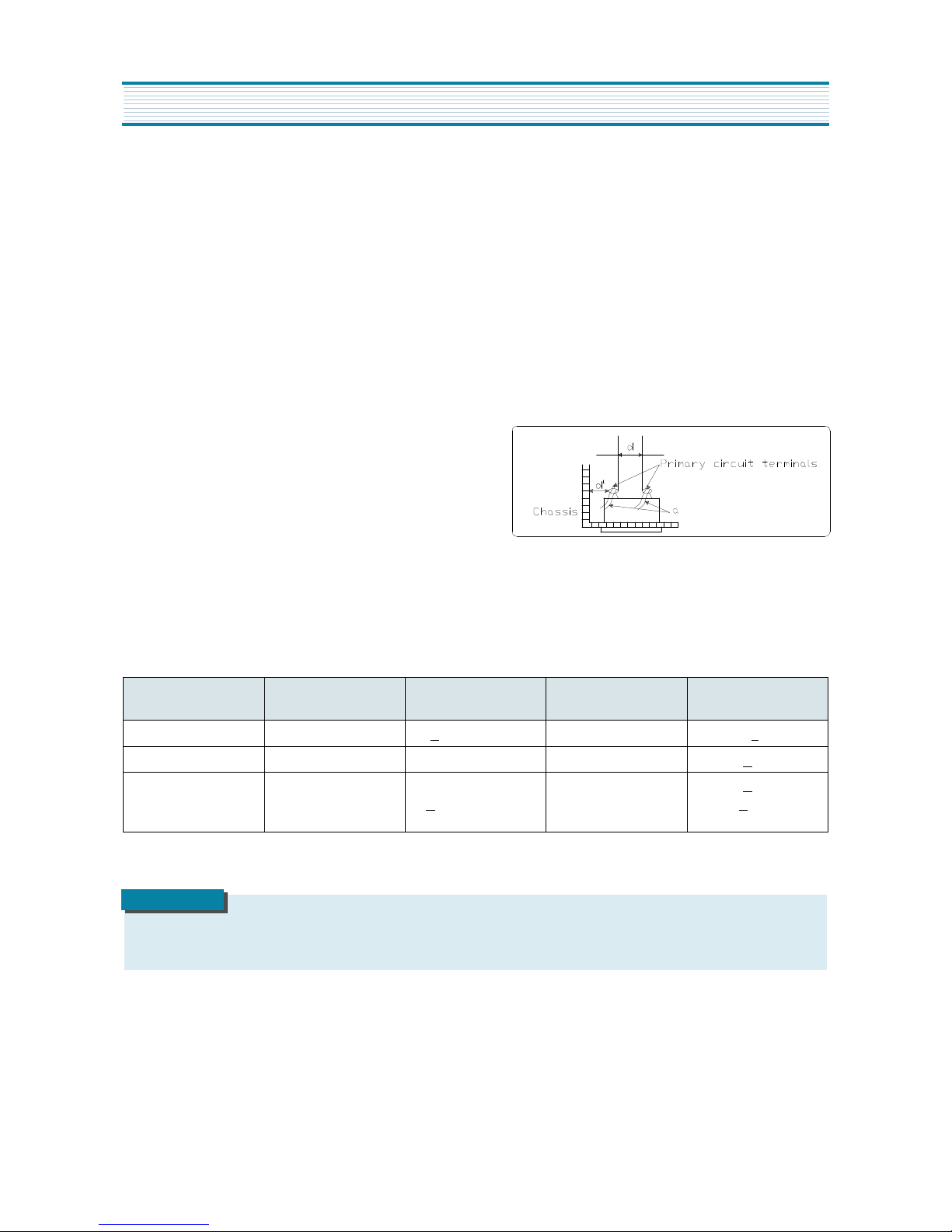
3. Clearance distance
When replacing primary circuit component, confirm specified clearance distance (d), (d
’
) between soldered terminals,
and between terminals and surrounding metallic parts. See table below.
Rating for selected areas
* : Class model only
AC Line Voltage Region
Insulation
Resistance
Dielectric
Strength
Clearance
Distance(d),(d)
100V Japan
>1MΩ
/500V DC
1kV AC 1min.
>
3
110 to 130V
USA & Canada
- 900V AC 1min.
>
3.2
* 110 to 130V
200 to 240V
Europe
Australia
Latin America
>10MΩ
/500V DC 4kV AC 1min.
>
6(d)
>
8(d')
(a :Power cord)
This table is unofficial and for reference only. Be sure to confirm the precise values for your
particular country and locality
NOTE
3
SAFETY & PRECAUTIONS
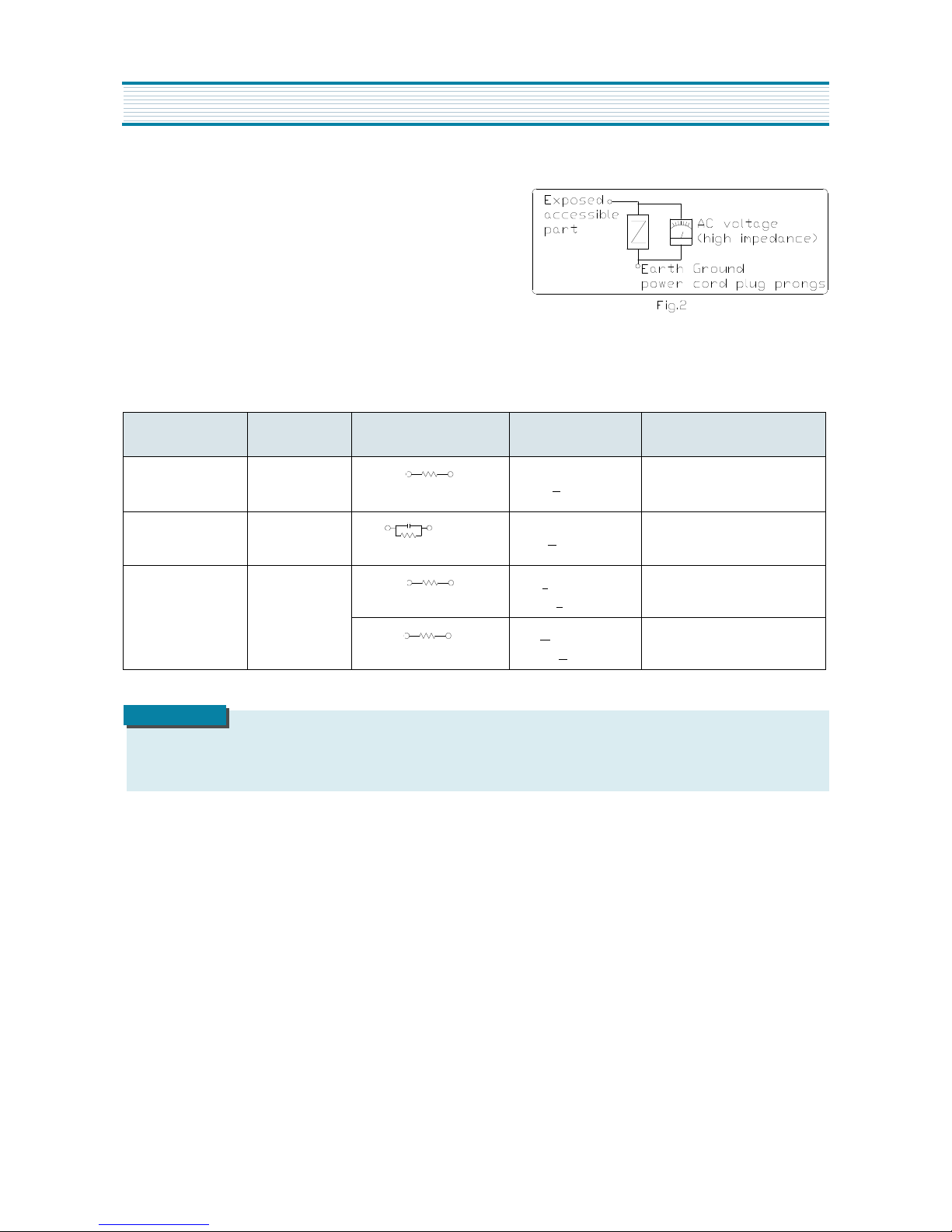
4. Leakage current test
Confirm specified or lower leakage current between B(earth
ground, power cord plug prongs) and externally exposed accessible parts (RF terminals, antenna terminals, video and audio input
output terminals, microphone jacks, earphone jacks, etc.)
Measuring method:(Power ON) Insert load Z between B(earth
ground, power cord plug prongs) and exposed accessible parts.
Use on AC voltmeter to measure across both terminals of load Z.
See figure2 and following table.
Leakage current ratings for selected are as
AC Line Voltage Region Load Z
Leakage Cur-
rent(i)
Clearance Distance(d),(d’)
100V Japan
1k
Ω
i
<
1 mArms
Exposed accessible parts
110 to 130V USA &Canada
15kmF
1k
Ω
i
<
0.5mArms Exposed accessible parts
110 to 130V
200 to 240V
Europe
Australia
2k
Ω
i
<
0.7mA peak
i
<
2mAdc
Antenna earth terminals
50k
Ω
i
<
0.7mA peak
i <
1mAdc
Other terminals
This table is unofficial and for reference only. Be sure to confirm the precise values
for your particular country and locality.
NOTE
4
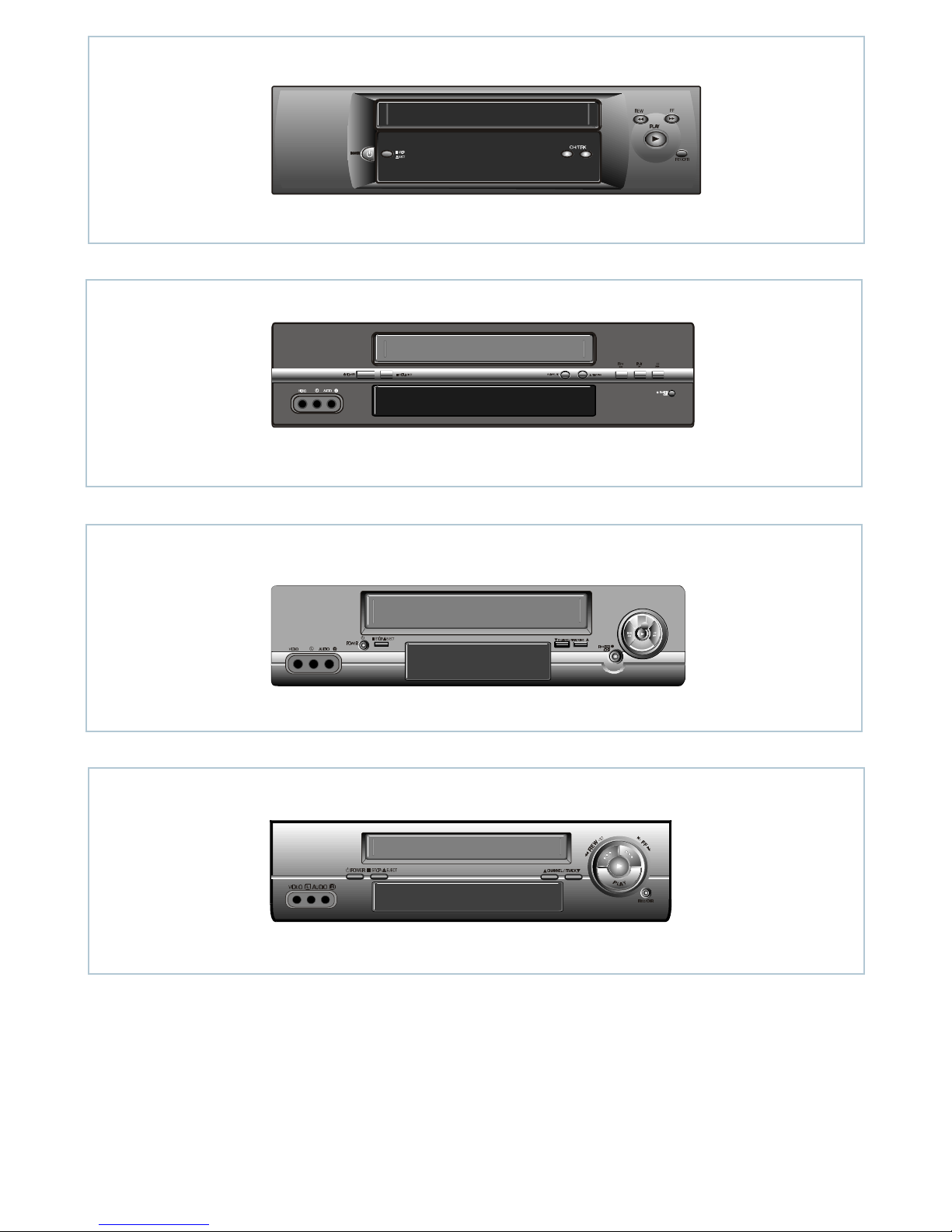
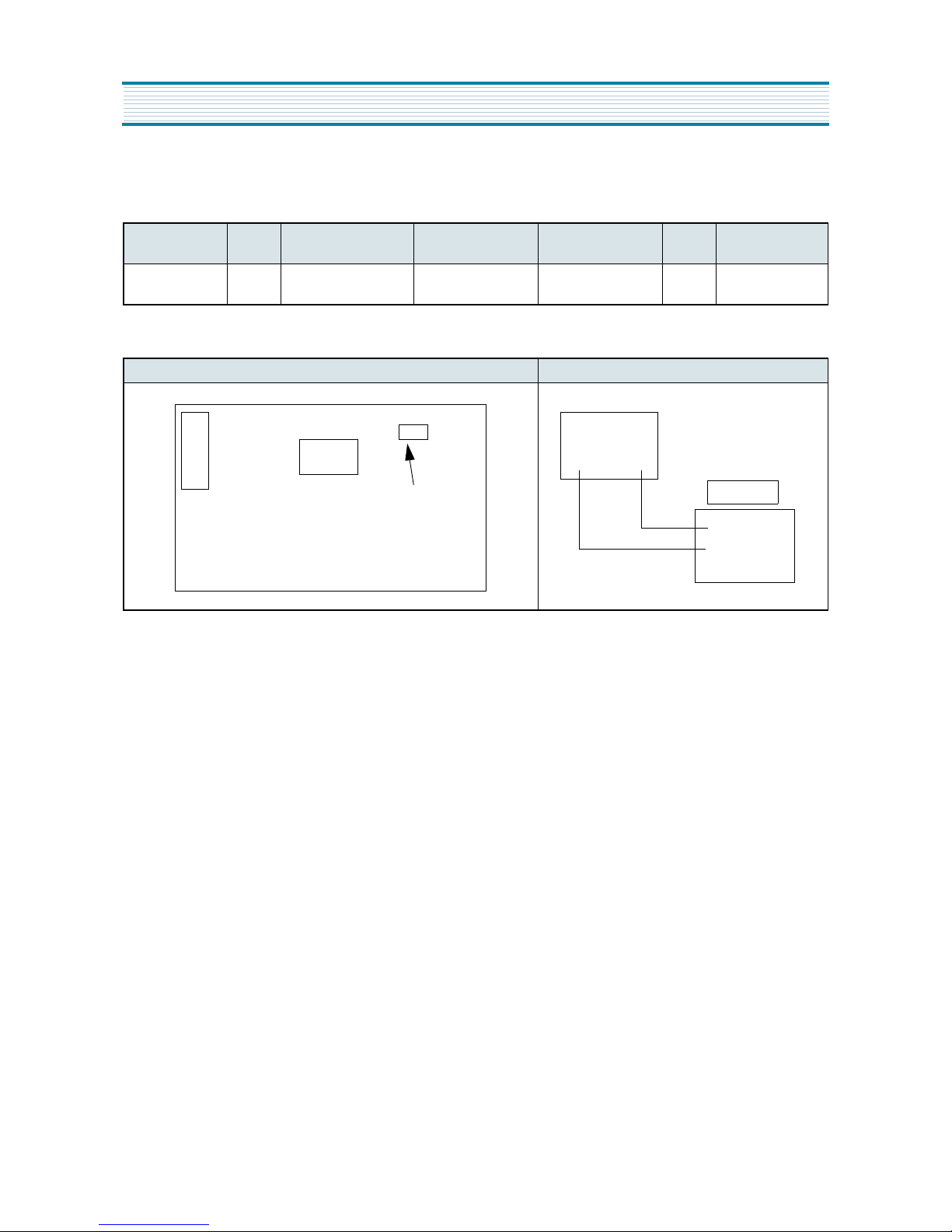
1. FRONT VIEWS FUNCTION
DVST7C3 FRONT VIEW
DVST7E3 FRONT VIEW
DVST7L3 FRONT VIEW
DVST7M3 FRONT VIEW
EXTERNAL VIEWS
EXTERNAL VIEWS
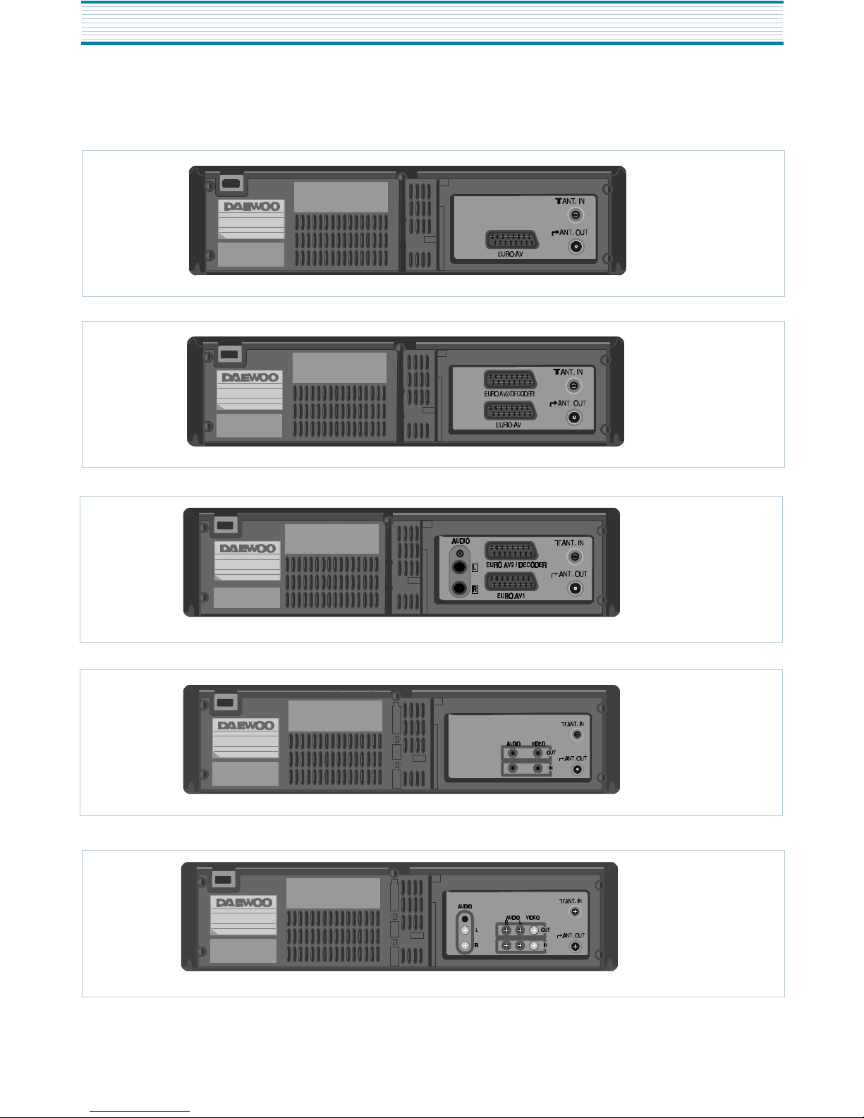
2. REAR VIEWS FUNCTION
MONO 1 SCART TYPE REAR VIEW
MONO 2 SCART TYPE REAR VIEW
HI-FI 2 SCART TYPE REAR VIEW
MONO RCA TYPE REAR VIEW
HI-FI RCA TYPE REAR VIEW
6
7
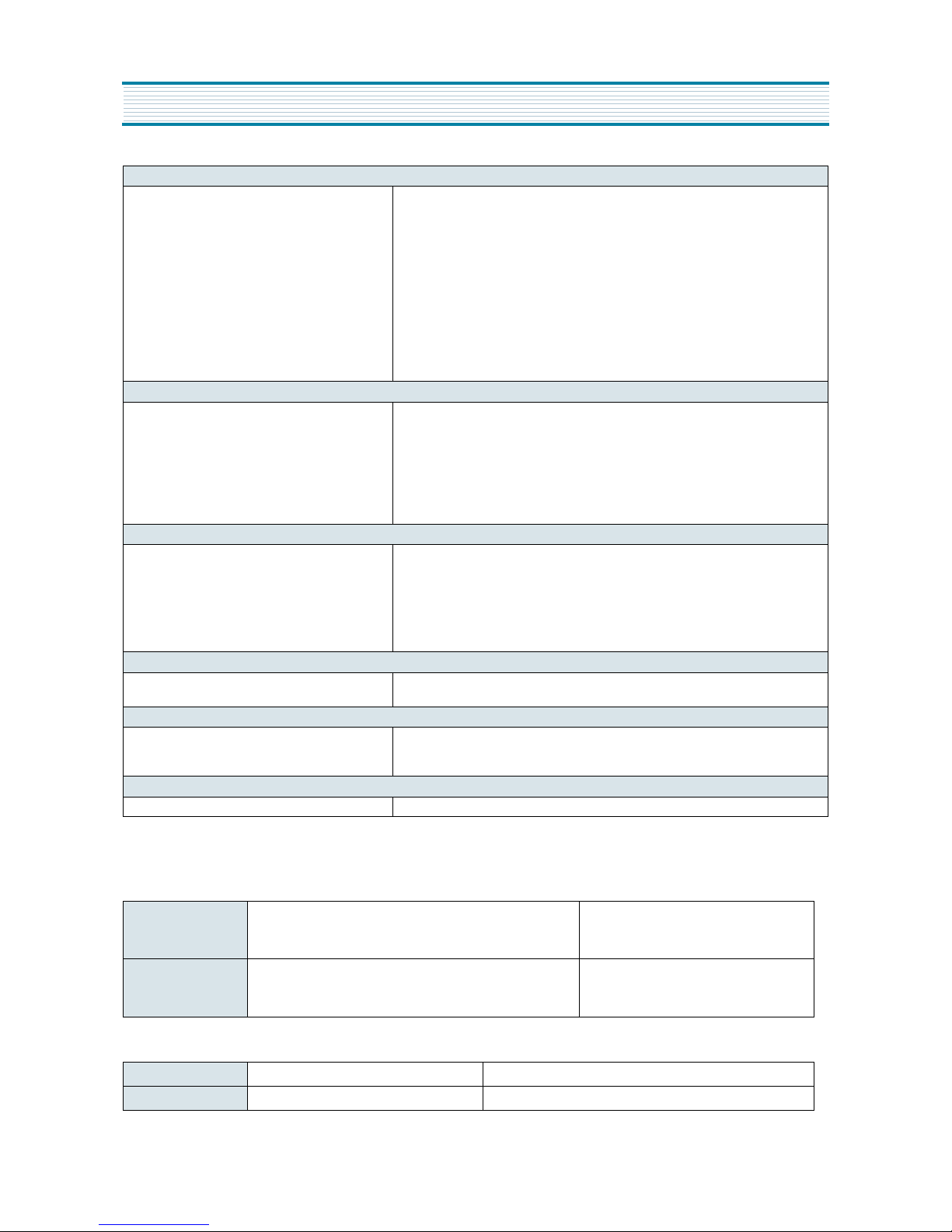
ELECTRICAL ADJUSTMENT
1. PLAYBACK PHASE
ADJUSTMENT PROCEDURE
1. Play back the test tape. (DP-2)
2. Set the oscilloscope to the CHOP mode. Connect CH1 to the SW PULSE (PIN 4 of P502)
3. Connect CH2 to the ENVE signal (PIN5 of P502)
4. Insert PATH JIG and press "REC" button on the remote control.
5. Check the position of the V-sync from the rising edge of the SW pulse.
(Standard : 6.5H ± 0.5H)
ITEM MODE
ADJUSTMENT
POINT
CHECK POINT
TEST
EQUIPMENT
TEST
TAPE
INPUT
SIGNAL
6.5H
ADJUSTMENT
PLAY [REC] BUTTON
PIN 4 & PIN 5
OF P502
OSCILLOSCOPE DP-2 NO SIGNAL
ADJUSTMENT PARTS MEASURING POINT
PCB : MAIN - TOP VIEW
TMI
BLOC
PREAMP
P502
TO PATH JIG
OSCILLOSCOPE
CH1 CH2
PATH JIG
8
SPECIFICATIONS
CHANNEL COVERAGE
INPUT/OUTPUT JACK TYPE
GENERAL
Power Requirement
Power Consumption
Temperature
Operating position
Dimensions (W x H x D)
Weight
Format
Tape Width
Tape Speed
Maximum Recording Time with full-size cassette
AC 230V, 50Hz
Max. 17W (in REC mode)
5×C ~ 35×C (Operating)
-20×C ~ 60×C
Horizontal only
360 x 90 x 288 (mm)
Approx. 3.85 Kg
VHS standard
12.65mm
(SP) : 23.39mm/sec
(LP) : 11.70mm/sec
(SP) :240min, with E-240 video cassette
(LP) :480min, with E-240 video cassette
VIDEO
Signal system
Recording system
Input
Output
Signal-to-Noise ratio
Horizontal resolution
PAL/SECAM colour and CCIR monochrome signals, 625 lines/50 fields
Rotary two-head helical scan with a slant double-azimuth combination video
head
1.0Vp-p, 75ohms, unbalanced
1.0Vp-p, 75ohms, unbalanced
45dB (Rhode & Schwarz noise meter) with NETTETE IMAGE control at center position
240 lines with NETTETE IMAGE control at center position
AUDIO
Recording system
Input
Output
Frequency Range
Signal to Noise Ratio
Audio Distortion
Longitudinal track
-8dBm, (CENELEC standard),more than 47 k-ohms, unbalanced
-6dBm, (CENELEC standard), less than 1k-ohms, unbalanced(100k-ohms,
load)
100Hz to 8,000Hz
More than 38dB
Less than 3% (SP)
TUNER
Tuning system
RF Output
Voltage synthesized tuner Programmable V/S 99CH (Hyper band)
UHF channel 21~69 (52)
TIMER
Memory programmable
Back up time
Clock exactness
99 CH
Less than 1 Hour
In accordance with the exactness of power supply frequency (50Hz)
ACCESSORIES
Provided Accessories Remote control unit, RF Cable, Battery
SYSTEM
SECAM-L
PAL, SECAM-B/G, PAL-I/I
PAL, SECAM-B/G, D/K, HYPER BAND
PAL-I
CHANNEL
VHF Ch 2~12
UHF Ch 21~69
CATV Ch X,Y,Z S1~S41
UHF Ch 21~69
Model
EUROPE Asia, South Africa, Australia
Jack Type
SCART Type RCA Jack (Phone Jack)
*
Design and specification can be subjected to change without notice.
9
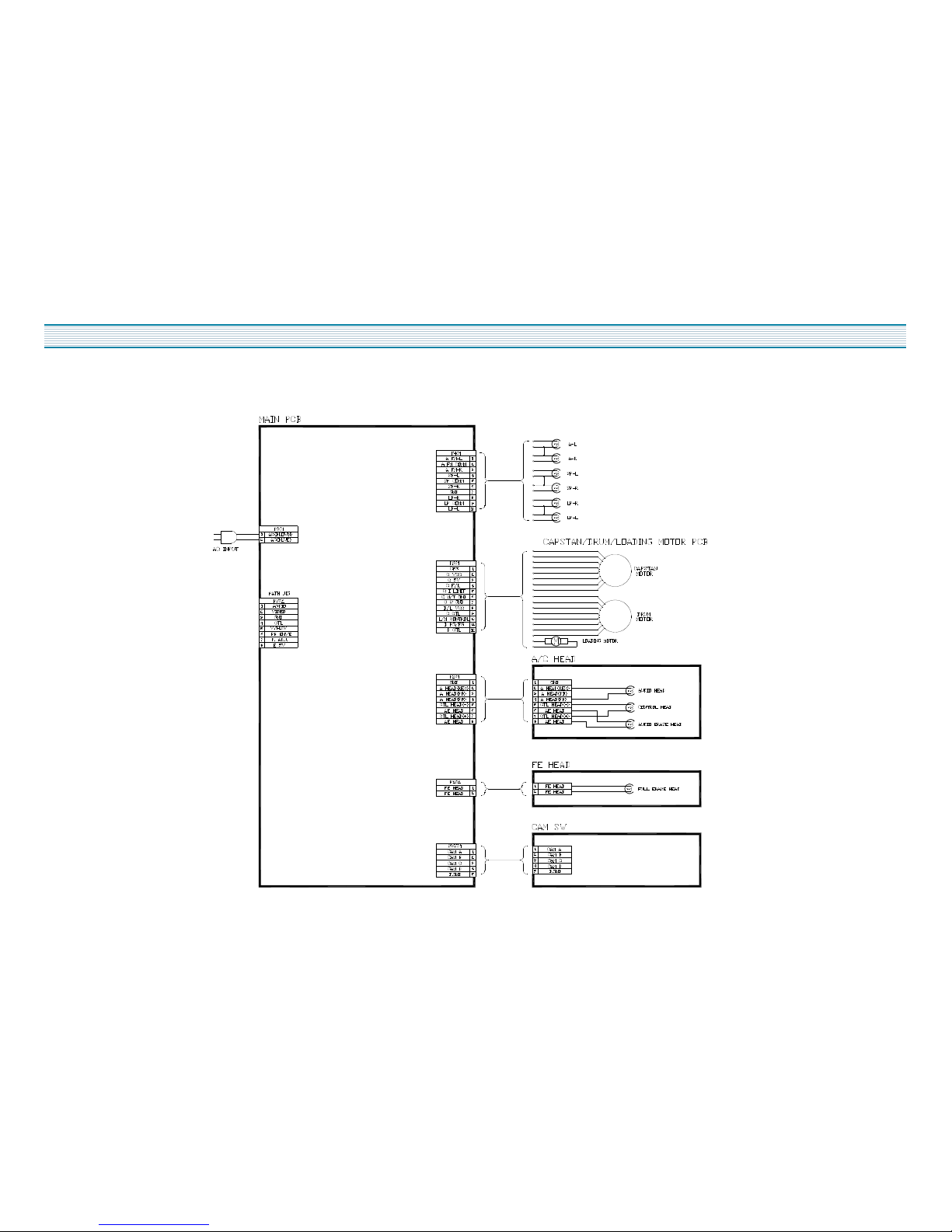
CIRCUIT INFORMATION
1. INTERCONNECT WIRING DIAGRAM
10
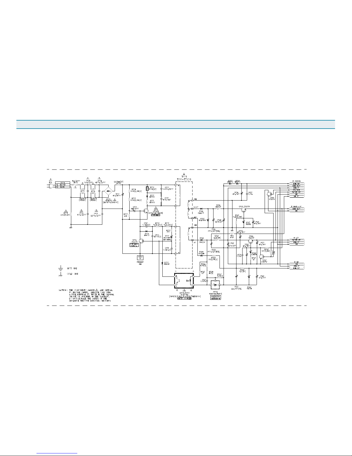
CIRCUIT INFORMATION
2. POWER CIRCUIT DIAGRAM
11
CIRCUIT INFORMATION
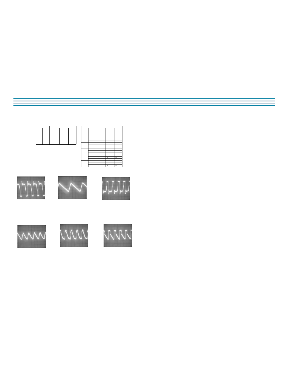
POWER MODE
LOC. PIN EE PLAY REC.
IC802 1 2.46 2.46 2.46
2 4.81 4.83 4.82
3 0 0 0.01
IC801 1 5.88 5.89 5.89
/803 2 4.81 4.83 4.83
3 0.25 0.25 0.25
4 3.1 3.1 3.1
POWER MODE
LOC. PIN EE PLAY REC.
Q801 E 0 0 0
B -0.12 -0.11 -0.72
C 323 323 323
Q802 E 0 0 0
B 0.25 0.26 0.17
C 0.12 0.11 0.17
Q821 E 12.58 12.6 12.6
B 13.2 13.2 13.2
C 15.6 15.36 15.4
Q822 E 5.2 5.19 5.2
B 5.89 5.89 5.89
C 5.97 5.97 5.96
Q825 E 0 0 0
B
C 5.89 5.89 5.89
Q826 E 0 0 0
B 0.73 0.73 0.73
C
1. T801 PIN 1 X : 0.1KV DIV
Y : 5uS DIV
2. T801 PIN 3 X : 2V DIV
Y: 2mS DIV
3. T801 PIN4 X: 5V DIV
Y: 5uS DIV
4. IC801 PIN3 X : 0.5V DIV
Y : 5uS DIV
5. IC801 PIN 4 X: 2V DIV
Y : 5uS DIV
6. Q801 base X: 0.5V DIV
Y : 5uS DIV
 Loading...