
Colour Television
CHASSIS : CP-490
MODEL : DTR-14D3VG
DTR-14D3TM
DTR-16D3VG
DTR-20D3VG
DTR-20D3TM
DTR-21D3TMW
DTR-21D3VGW
DTR-21D3TGW
DAEWOO ELECTRONICS CO., LTD.
S/M No:CP490P-010
✔
Caution
: In this Manual, some parts can be changed for improving, their
performance without notice in the parts list. So, if you need the
latest parts information,please refer to PPL(Parts Price List) in
Service Information Center (http://svc.dwe.co.kr).

CONTENTS
Specifications ................................................................................................ 1
Safety Instruction .......................................................................................... 2
Circuit block Diagram .................................................................................... 3
Alignment Instructions ................................................................................. 4
IC Description ................................................................................................ 8
Circuit Description ....................................................................................... 34
Trouble Shooting Charts ............................................................................. 49
Electrical Parts List ..................................................................................... 56
CP-490 each model Parts List .................................................................... 62
Mechanical Exploded View and Parts List ................................................ 64
PCB Layouts ................................................................................................ 67
• PRINTED CIRCUIT BOARDS
• SCHEMATIC DIAGRAM
1
Specifications
TV Standard PAL/SECAM-B/G, D/K, I, H, NTSC-3.58/4.43
Mains Voltage 100~250V AC, 50/60Hz
Power Consumption 14”, 16” = 85W
20”, 21” = 90W
Sound output . 2 Speaker (at 80% MOD. 10% THD) : 5W + 5W (TWITTER 2.5W + 2.5W) 14”, 16”
6W + 6W (TWITTER 2.5W + 2.5W) 20”
. 3 Speaker (at 80% MOD. 10% THD) : 8W + 8W + 8W(21”)
Speaker . 2 Speaker : 7.5W, 8 OHM(2EA)
. 3 Speaker : 12W, 8 OHM(3EA)
Antenna 75 ohm unbalanced
Impedance 300 ohm balanced with supplied balun
Tuning system Voltage Synthesize Tuning System
Memory channel 100 channels
Reception VHF - L : CH2 - CH4
channel Unit VHF - H : CH5 - CH12
Cable Band : CHS1’ - CHS3’, CHS1 - CHS20
UHF : CH21 - CH69
Remote control VG : R-28B04, TM : R-28B03
Screen size 14” : 34cm (A34JLL 90 02)
20” : 48cm (A48JLL 90 02)
21” : 51cm (A51JLL 90 02)
Weight 14” : 9.7Kg(set)
20” : 19.6Kg(set)
21” : 26.5Kg(set)
Indication On-Screen Display
- MENU
• Picture (Brightness, Color, Contrast, Sharpness, TINT)
• TIMER (TM/TMW/TGW:CLOCK, OFF TIME, WAKE-UP-TIME, ACTIVATE, WAKE-UPPROG/VG:CLOCK, ON TIME, OFF TIME)
• LANGUAGE
• PRESET
• EDIT (TM, TMW, TGW)
• SLEEP •BLUE BACK •GAME
• AV1, AV2 •NORMAL1, NORMAL2, FAVORITE
• SOUND MUTE
• VOLUME CONTROL
• WOOFER (21” ONLY)
• 16:9, ZOOM, NORMAL
VG : WITHOUT TXT. MODEL, TM : WITH TXT. MODEL

2
Safety Instruction
WARNING: Before servicing this chassis, read the “X-RAY RADIATION precaution”, “safety precaution”
and “product safety notice” below.
1. Excessive high voltage can produce potentially
hazardous X-RAY RADIATION.To avoid such
hazards, the high voltage must not exceed the
specified limit. The nominal value of the high
voltage of this receiver is 23-24kv(14”), 2627kv(20”, 21”) at max beam current. The high
voltage must not, under any circumstances,
exceed 27.5kv (14", 20”), 29.0kv(21”).
Each time a receiver requires servicing, the high
voltage should be checked. It is recommended
the reading of the high voltage recorded as a part
of the service records. it is important to use an
accurate and reliable high voltage meter.
2. The only source of X-RAY Radiation in this TV
receiver is the picture tube. For continuous
RADIATION protection, the replacement tube
must be exactly the same type tube as specified
in the parts list.
1. Potentials of high voltage are present when this
receiver is operating. Operation of the receiver
outside the cabinet or with the back cover
removed involves a shock hazard from the
receiver.
1) Servicing should not be attempted by anyone
who is not thoroughly familiar with the
precautions necessary when working on highvoltage equipment.
2) Always discharge the picture tube to avoid the
shock hazard before removing the anode cap.
3) Discharge the high potential of the picture tube
before handling the tube. The picture tube is
highly evacuated and if broken, glass
fragments will be violently expelled.
2. If any Fuse in this TV receiver is blown, replace it
with the FUSE specified in the Replacement
Parts List.
3. When replacing a high wattage resistor(oxide
metal film resistor) in circuit board, keep the
resistor 10mm away from circuit board.
4. Keep wires away from high voltage or high
temperature components.
5. This receiver must operate under AC260 volts,
50Hz/60Hz. (AC 100~250 volts, 50/60Hz)NEVER
connect to DC supply or any other power or
frequency.
Many electrical and mechanical parts in this
chassis have special safety-related characteristics.
These characteristics are often passed unnoticed
by a visual inspection and the X-RAY RADIATION
protection afforded by them cannot necessarily be
obtained by using replacement components rated
for higher voltage, wattage, etc.
X-RAY RADIATION PRECAUTION
PRODUCT SAFETY NOTICE
SAFETY PRECAUTION
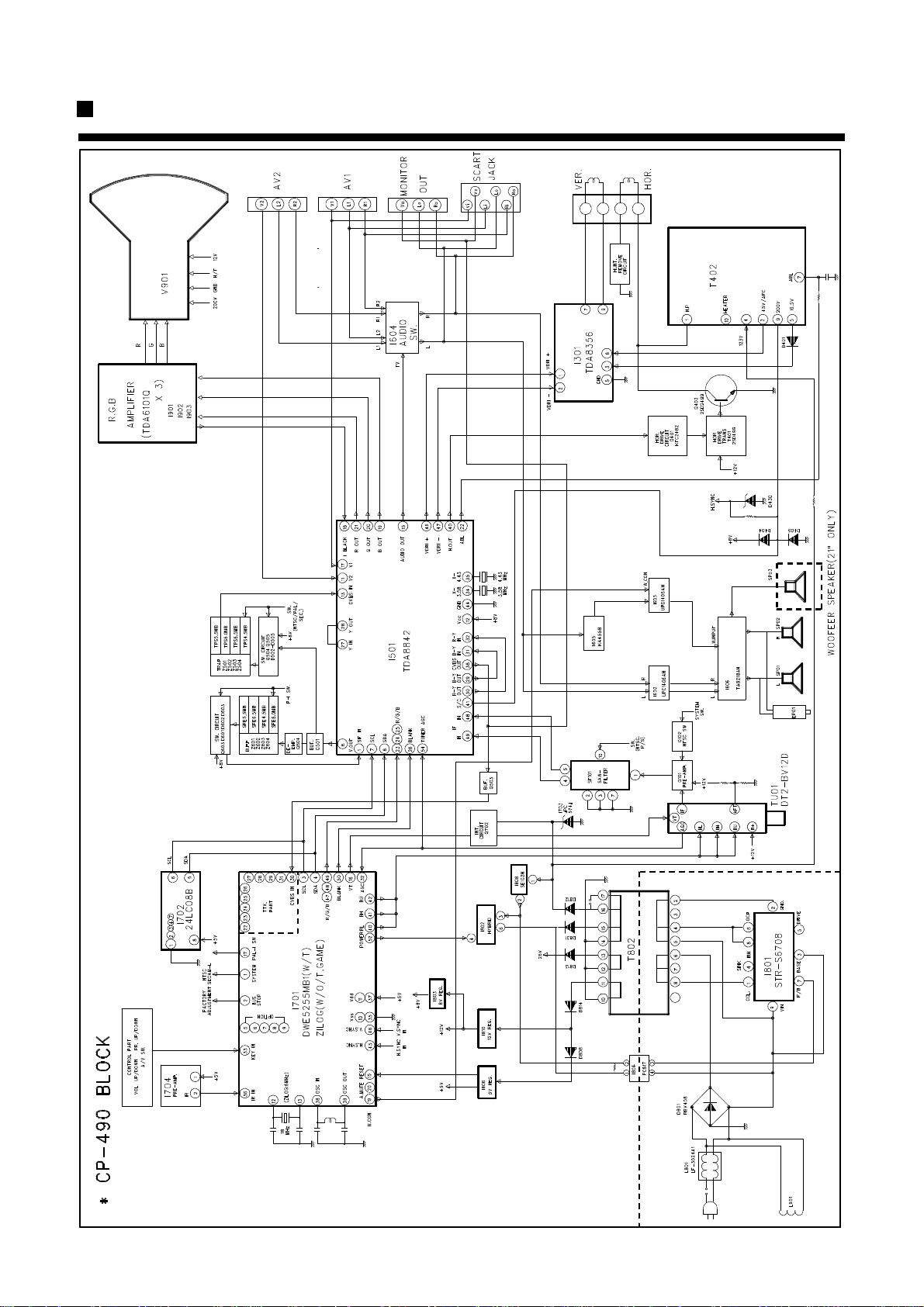
Circuit Block Diagram
3
4
1. AFT
1.1 Standard B/G,D/K,I
1) Set a Signal Generator with
- RF FREQUENCY = 38.9 MHz,
- RF OUTPUT LEVEL = 80 5 dBuV
- System = PAL / SECAM - B/G, D/K, I
NTSC - 3.58/4.43
2) Connect the Signal Generator RF Output to P101 (Tuner IF Output).
There must be no signal input to the tuner.
3) Press the “AFT” KEY and wait until the TV screen display “AFT OK”.
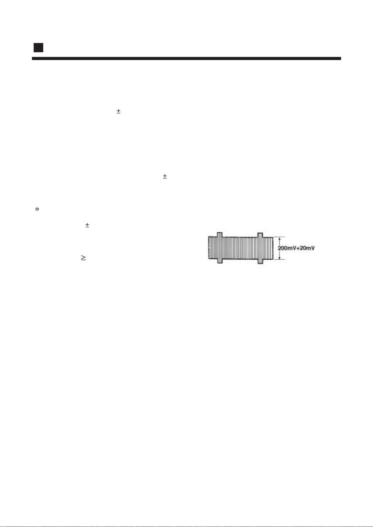
2. AGC
1) Set a Pattern Generator with RF LEVEL 63° 2 dBuV .
2) Connect a OSCILLOSCOPE PROBE to P102 (TUNER AGC INPUT).
3) Adjust AGC UP/DOWN KEY the voltage drop 2.0V±0.5V dc point its maximum voltage.
Alternative Method
1) Set a Pattern Generator with
- RF LEVEL 80 5 dBuV
- PAL CROSSHATCH
( without SOUND CARRIER )
2) Connect a OSCILLOSCOPE
( Bandwidth 100MHz ) PROBE
to P101 (TUNER IF OUTPUT).
3) Use AGC UP/DOWN KEY to obtain
an envelop amplitude 200 + 20 mVp-p.
3. SCREEN
1) Receive the color bar pattern and heat run over 15
minutes.
2) On the normal mode1 adjust the screen volume that
the horizontal line appears on the screen after pushing the AFT-L key on the SVC remote control unit.
3) Adjust the screen volume that the horizontal lines
reach the cut-off point
4. WHITE BALANCE
1) Set the TV to NOR I mode.
2) Set the R,G,B LEVEL to CENTER with R,G,B UP/DOWN KEY .
3) Adjust the R,G,B UP/DOWN KEY of the color which appears abnormally
on the screen to obtain WHITE BALANCE.
5. FOCUS
1) Apply a RETMA PATTERN signal.
2) Adjust the FOCUS VOLUME on FBT to obtain optimal resolution.
Alignment Instructions
5
6. GEOMETRY
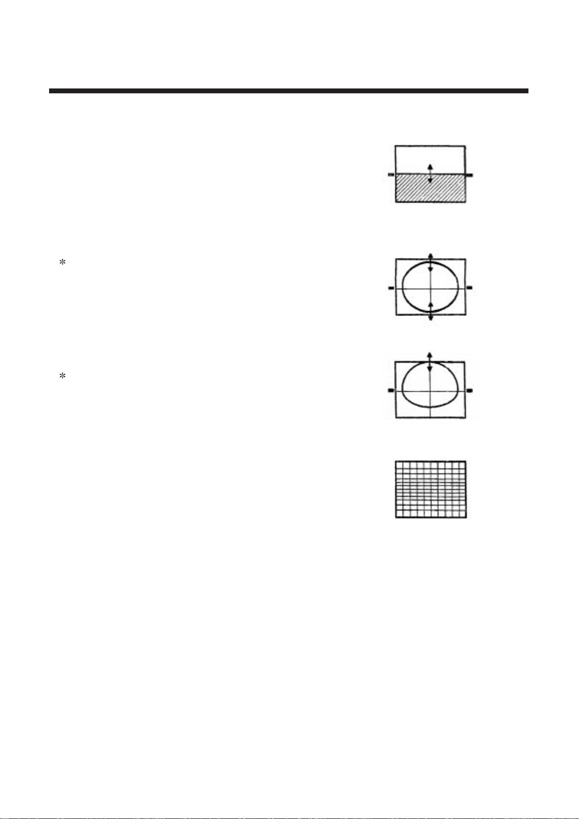
6.1 VERTICAL CENTER
1) Set the TV to NOR I mode.
2) Pressing the V-SIZE UP/DOWN KEY, the
lower half of the screen is blanked.
3) Adjust the border line of blanked picture
coincident with the mechanical center marks
of the CRT using the V-CENTER UP/DOWN KEY.
6.2 VERTICAL SIZE
The VERTICAL CENTER adjustment
has to be done in advance.
1) Apply a RETMA PATTERN signal.
2) Set the TV to NOR I mode.
3) Adjust the upper part of the picture
with the V-SIZE UP/DOWN keys.
6.3 VERTICAL SLOPE
The VERTICAL SIZE adjustment
has to be done in advance.
1) Apply a RETMA PATTERN signal.
2) Adjust the lower part of the picture
with the V-SLOPE UP/DOWN keys.
6.4 VERTICAL S-CORRECTION
1) Apply a CROSSHATCH PATTERN signal.
2) Adjust the S-COR UP/DOWN KEY to obtain
the same distance between horizontal lines.
6.5 HORIZONTAL CENTER
1) Apply a RETMA PATTERN signal.
2) Adjust picture centering with H-CENTER
LEFT/RIGHT keys.

6
If EEPROM(I702) has been changed ;
- Option data has to be changed and
- all alignment function has to be readjusted.
The initial state of adjustment are as follows;
- V-Center, V-Slope V-Size, H-Center, R, G, B, AFT = Center (30/64 - 33/64)
- S-Correction = 00/64
- AGC = 15~60/64
Service Remocon

7
IC Description
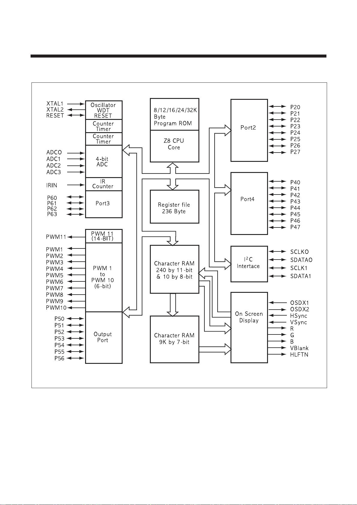
DW90244-AS/(Z8 DIGITAL TELEVISION CONTROLLER)
= Z9024106PSC (ZILOG TYPE NO.)
(1) General Description
The Z9023X Digital Television Controller (DTC) family is ZILOG’s latest and most powerful Z8-based DTC product offering,
These parts feature larger system RAM and Rom Options, together with a host of new features including a newcolor palette
systen, flexible inter-row spacing, higher character cell resolution, background mesh effect, dedicated I. R. capture registers,
on-chip Analog-to-Digital conversion, and a hardware Master mode I
2
C interface. The famililiar Z8 core in combination with
these advanced features makes the Z9023X family an ideal choice for low to midrange televisions in both PAL and MTSC
markets.
The Z9023X family consists of three basic device types; ICE Chip (Z90239), ROM Mask Parts (Z90233/Z90234), and OTP
Part (Z90231), The OTP (Z90231) supports field programmable 32KB system ROM. ICE Chip (Z90239) is used in Z90239
Emulator and ProtoPaK. As described above, Z90233 supports 16KB system ROM and Z90234 supports 24KB system
ROM for mask.
The Z9021X family takes full advantage of the Z8’s expanded register file space to offer greater flexibility in On Screen Display creation.
(2) Feature
Z8-Based CMOS Microcontroller for Consumer Television, Cable Box, and Satellite Receiver Applications
• 42 - Pin SDIP Package except Z90239 (124 PGA)
• Z8@MCU Core at 6 MHz
• Mask ROM sizes Available in 16 and 24KB
• Ten 6-bit Pulse Width Modulators
• One 14-bit Pulse Width Modulator
• On-Chip Infrared (IR) Capture Registers
• Four Channel 4-bit Analog-to-Digital Converter
• Twenty Seven General Purpose I/O Pins
• I2C Master Serial Communication Port
On Screen Display (OSD) Section
• Supports Displays up to 10 rows by 24 Columns with 256 Characters
• Character Cell Resolution of 14 Pixels by 18 Scan lines
• Variable Inter-row Spacing from 0-15 Horizontal Scan Lines
• Foreground and Background Colors Fully Programmable by Character
8
(3) Block Diagram

1 P40 P47/PWM10 42
2 P20 P46/PWM9 41
3 P21 F BLANK 40
4 P22 B 39
5 P23 G 38
6 P24(SCLØ) R 37
7 P25(SDAØ) V-SYNC 36
8 P26(SCL1) H-SYNC 35
9 P27(SDA1) P63 34
10 GND P45/PWM8 33
11 VCC P44/PWM7 32
12 X-TAL1 P43 31
13 X-TAL2 P42 30
14 P55/PWM6 OSD X2 29
15 RESET OSD X1 28
16 P56/PWM6 VCC 27
17 P54/PWM5 IR IN 26
18 P53/PWM4 AGND 25
19 P52/PWM3 P62/ADCO 24
20 P51/PWM2 P61/ADC2 23
21 P50/PWM1 P60/ADC3 22
9
(4) PIN CONFIGURATION(Z90241)
(5) PIN DESCRIPTION
Table 1. Z90231/233/234 42-Pin SDIP Package
NOTE : 1. It is input on POR. It must be configured to be output ports for PWM applications
Pin Number Pin Function I/O/PWR Reset State Name Note
34 +5 Volts PWR PWR Vdd
30, 13 0 Volts PWR PWR Vss, AVss
36 Infra Red remote capture input I I IRIN
1 14-bit Pulse Width Modulator output O I PWM11 1
20, 19, 18, 17, 2, 3, 4, 5, 6 ,7 6-bit Pulse Width Modulator output O I PWM [10:1] 1
7, 6, 5, 4, 3, 2, 1 Bit programmable Input/Output ports I/O I P5 [6:0]
42, 41, 40, 39, 38, 37, 35, 21 Bit programmable Input/Output ports I/O I P2 [7:0]
21 Half tone output O I HLFTN
40, 42 I
2
C Data I/O I SDATA0, 1
39, 41 I
2
C Clock I/O I SCLK0, 1
16, 12, 10, 9 Bit programmable Input/Output ports I/O I P6 [3:0]
20, 19, 18, 17, 15, 14, 11, 8 Bit programmable Input/Output ports I/O I P4 [4:0]
31 Crystal oscillator Input I I XTAL1
32 Crystal oscillator output O O XTAL2
28 Dot clock oscillator Input I I OSDX1
29 Dot clock oscillator output O O OSDX2
26 Horizontal Sync I I HSYNC
27 Vertical Sync I I VSYNC
25 Video blank O O CBLANK
24, 23, 22 Video R, G, B O O R, G, B
9, 10, 11, 12 4-bit Analog to Digital converter input AI I ADC[3:0]
33 Device reset I I /RESET

10
DW5255MBI
(TVTEXT 8-bit Micro controller , Rom-version)
=SDA5254 (SIEMENS Type No.)
(1) General Description
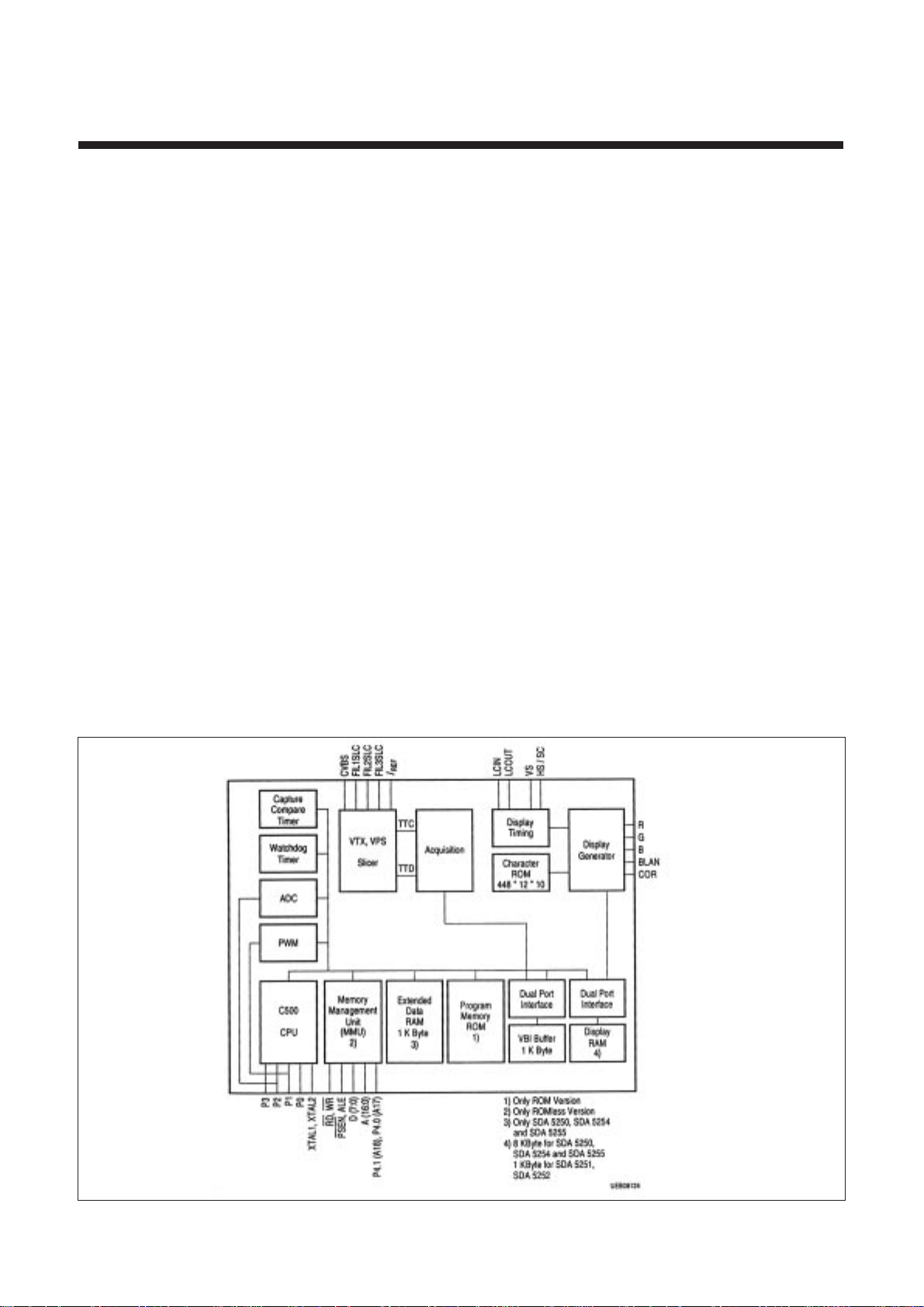
The SDA 525x contains a slicer for TTX, VPS and WSS, an accelerating acquisition hardware modul, a display generator for “Level 1” TTX data and an 8 bit microcontroller running at 333 ns cycle time. The controller with dedicated hardware guarantees flexibility, does most of the internal processing of TTX acquisition, transfers data to/from the external
memory interface and receives/transmits data via I2C and UART user interfaces. The block diagram shows the internal
organization of the SDA 525x. The Slicer combined with dedicated hardware stores TTX data in a VBI buffer of 1 Kbyte.
The microcontroller firmware does the total acquisition task (hamming- and parity-checks, page search and evaluation
of header control bits) once per field.
(2) Feature
•
Acquisition:
- Feature selection via special function register
- Simultaneous reception of TTX, VPS and WSS
- Fixed framing code for VPS and TTX
- Acquisition during VBI
- Direct access to VBI RAM buffer
- Acquisition of packets X/26, X/27, 8/30 (firmware)
- Assistance of all relevant checks (firmware)
- 1-bit framing code error tolerance (switchable)
•
Display:
- Features selectable via special function register
- 50/60 Hz display
- Level 1 serial attribute display pages
- Blanking and contrast reduction output
- 8 direct addressable display pages for SDA 5250, SDA 5254 and SDA 5255
- 1 direct addressable display pages for SDA 5251 and SDA 5252
- 12 x 10 character matrix
- 96 character ROM (standard G0 character set)
- 143 national option characters for 11 languages
- 288 characters for X/26 display
- 64 block mosaic graphic characters
- 32 characters for OSD in expanded character ROM + 32 characters inside OSD box
- Conceal/reveal
- Transparent foreground/background - inside/outside of a box
- Contrast reduction inside/outside of a box
- Cursor (colour changes from foreground to background colour)
- Flash (flash rate 1s)
- Programmable horizontal and vertical sync delay
- Full screen background colour in outer screen
- Double size / double width / double height characters
•
Synchronization:
- Display synchronization to sandcastle or Horizontal Sync (HS) and Veritical Sync (VS) with start-stop-oscillator
- Independent clock systems for acquisition, display and controller
11
• Micro
controller
- 8 bit C500-CPU (8051 compatible)
- 18 MHz internal clock
- 0.33 µs instruction cycle
- Eight 16-bit data pointer registers (DPTR)
- Two 16-bit timers
- Watchdog timer
- Capture comprare timer for infrared remote control decoding
- Serial interface (UART)
- 256 bytes on-chip RAM
- 8 Kbyte on-chip on-chip display-RAM (access via MOVX) for SDA 5250, SDA 5254 and SDA 5252
- 1 Kbyte on-chip display-RAM (access via MOVX) for SDA 5250, SDA 5254 and SDA 5255
- 1 Kbyte on-chip TVT/VPS-Acquisition-buffer-RAM (access via MOVX)
- 1 Kbyte on-chip extended-RAM (access via MOVX) for SDA 5250, SDA 5254 and SDA 5255
- 6 channel 8-bit pulse width modulation unit
- 2 channel 14-bit pulse width modulation unit
- 4 multiplexed ADC inputs with 8-bit resolution
- One 8-bit I/O port with open drain output and optional I2C-Bus emulation (PORT 0)
- Two 8-bit multifunctional I/O ports (PORT 1, PORT3)
- One 4-bit port working as digital or analog inputs (PORT 2)
- One 2-bit I/O port with optional function
- One 3-bit I/O port with optional RAM/ROM address expansion up to 512 Kbyte (ROMIess-Version)
•
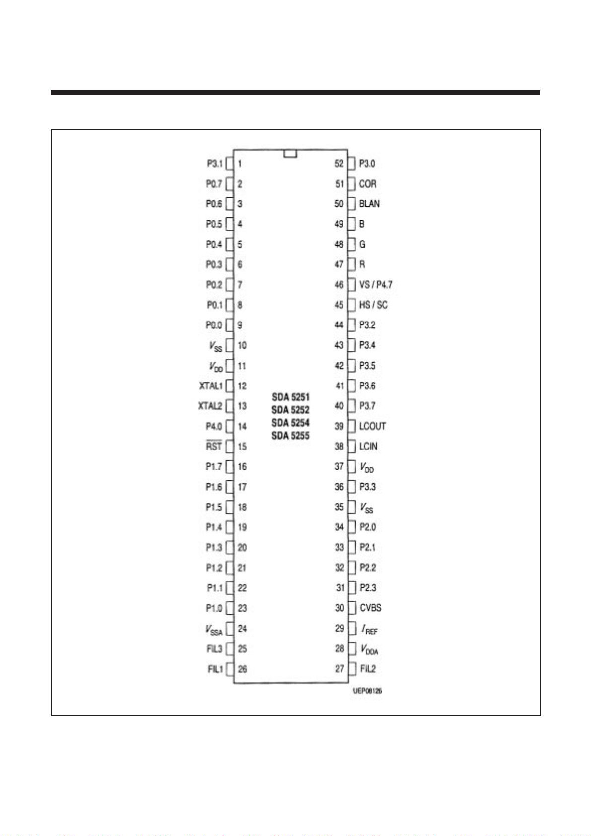
P-SDIP-52-1 package or P-MQFP-64-1 for ROM-Versions (SDA 5251, SDA 5252, SDA 5254, SDA 5255)
•
P-MQFP-80-1 Package for ROMIess-Version (SDA 5250 M)
•
P-LCC-84-2 Package for Emulator-Version (SDA 5250)
•
5 V Supply Voltage
(3) Block Diagram
12
(4) Pin Configuration P-SDIP-52-1 (ROM-Versions)
Pin Configuration P-SDIP-52-1 (ROM-Versions)
(top view)
24LC08B (EEPROM)
(1) Features
(2) General Description
The Microchip Technology Inc. 24LC08B is a 8K-bit Electrically Erasable PROM.
The device is organized as four blocks of 256x9bit memory with a two wire serial interface. Low voltage
design permits operation down to 2.5 volts with standby and active currents of only 5 A and 1mA respectively.
The 24LC08B also has a page-write capability for up to 16 bytes of data.
The 24L08B is available in the standard 8-pin DIP surface mount 80IC packages.
(3) Block Diagram
(4) Pin Description
PIN SYMBOL DESCRIPTION
1-3 A0, A1, A2 Device Address lnputs
4 Vss Ground
5 SDA Serial Data/Address
6 SCL Serial Clock
7WP
8 Vcc +5V Power supply
13
WP
SDA SCL
V
CC
VSS
I/O
CONTROL
LOGIC
MEMORY
CONTROL
LOGIC
XDEC
EEPROM ARRAY
(4X256X8)
PAGE LATCHES
SENSE AMP
R/W CONTROL
HV GENERATOR
YDEC
• Single supply with operation down to 2.5V
• Low power CMOS technology
- 1mA active current typical
- 10 A standby current typical at 5.5V
- 5 A standby current typical at 3.0V
• Organized as two or four blocks of 256 bytes
(2x256x8) and (4x256x8)
• Two wire serial interface bus, I2CTMcompatible
• Schmitt trigger, filtered inputs for noise suppression
• Output slope control to eliminate ground bounce
• 100KHz(2.5V) and 400KHz(5V) compatibility
• Self-timed write cycle(including auto-erase)
• Page-write buffer for up to 16 bytes
• 2ms typical write cycle time for page-write
• Hardware write protect for entire memory
• Can be operated as a serial ROM
• Factory programming(QTP) available
• ESD protection > 4,000V
• 1,000,000 ERASE/WRITE cycles(typical)
• Data retention > 40 years
• 8-pin DIP, 8-lead or 14-lead SOIC packages
• Available for extended temperature ranges
- Commercial : 0 C to +70 C
-Industrial : -40 C to +85 C

14
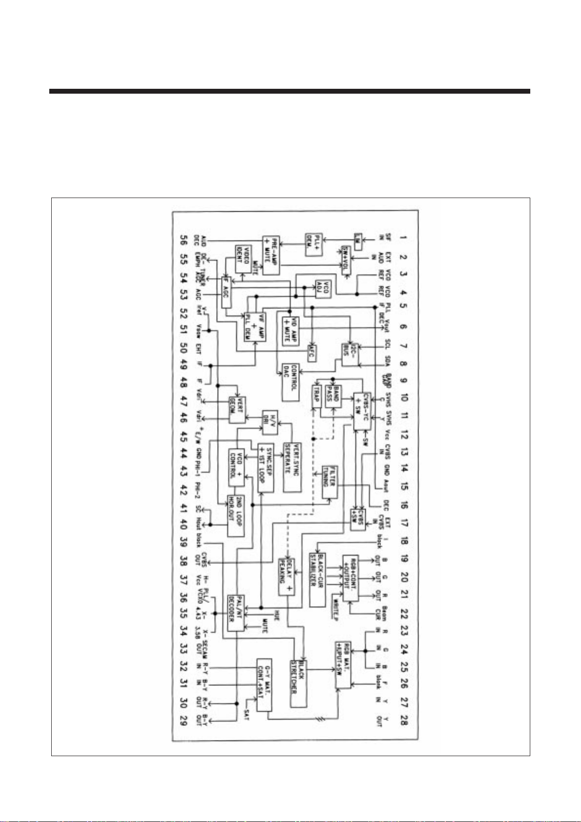
TDA884X ( One Chip TV -processor )
(1) General Description
The TDA884X family is a pin-aligned range of single chip video and audio processors.
With this family it is possible to cover in one layout a whole range of applications from simple small screen single standard
sets (as well PAL as NTSC with built-in delay line) to full multi-standard (including SECAM) 16:9 sets. Switching from the
TDA837x family to TDA884X family has been made very easy:the SDIP packages of the families are almost pin aligned and
minimal layout adaptations are necessary. Omitting the delay line TDA4665 and SECAM add-on TDA8395 with surrounding
components, VCO coil, direct connection of U, V in-and outputs and adapting the software to access the 5 extra registers
are the most relevant changes needed.
(2) Feature
• IF
- Alignment free IF-PLL, IF frequency selection via I2C (no external coil needed)
- Vision IF amplifier with high sensitivity and good figures for differential phase and gain
- PLL demodulator with high linearity offering the possibility for (single standard) intercarrier stereo audio application
- Alignment PLL via I2C
• AUDIO
- Alignment free multi standard PLL audio demodulator (4.5 to 6.5 MHz.)
- Volume control
• Video
- Integrated fixed luminance delay line
- Integrated chroma trap (auto calibrated)
- Integrated chroma bandpass filters with switchable centre frequency (auto calibrated)
- Asymmetrical peaking circuit in the luminance channel with switchable noise coring function
- Black stretching of non standard CVBS or luminance signals, switchable via I
2
C bus
• RGB
- RGB control (brightness, contrast, saturation)
- Improved black current stabilisation (continuos cathode calibration)
- White point adjustment
- Blue stretch which offsets colours near white to blue
- Option to insert “blue back” when no video signal is available
• Input / Output
- Flexible video source select with CVBS input for the internal signal and two external video inputs(one switchable for
CVBS or Y/C).
- The output signal of the video source select is externally available ( also as CVBS when Y/C input is used).
- External audio input.
- Linear RGB input with fast blanking.
• Synchronization and Deflection
- Horizontal synchronization with two control loops and alignment free horizontal oscillator.
- Slow start and slow stop of the horizontal drive output to enable low stress start-up and switch-off from the line
circuit at nominal line supply voltage.
- Vertical count-down circuit for stable behavior with provisions for non-standard signals.
- Vertical geometry control.
- Vertical drive optimized for DC coupled vertical output stages.
- Option for blanking of PAL plus helper signal
- Option to stop the vertical deflection for Vg2 alignment
- Option to switch-off in the vertical overscan
• Control
- Full I2C bus control, as well for customer controls as for factory alignment.
15
- All automatic controls have an option for forced mode.
• Power consumption
- Low power consumption.
• Packaging
- SDIP-56 (Shrinked Dual In Line Package, 56 pins).
(3) Block Diagram

16
(4) Pin Description
No Name Description
1 SOUND IF INPUT The sound equivalent input impedance is 8k5 ohm // 5pF which has to be
taken into account for proper termination of the ceramic filters.
The DC impedance is very high.
The minimum input signal for catching is l mV rms.
2 EXT AUDIO INPUT An external sound signal (500mVrms) for example from SCART can be applied to this
pin via a coupling capacitor. The input has been made suitable to allow maximum
2Vrms. The input impedance is 25kohm.
3 VCO REF FILTER The IF VCO tuned circuit is applied to these pin.
4 Its resonance frequency must be two times the IF-frequency and in between a
range of 64-120MHz.
This range is suitable for the IF standards as 33.4, 38.9, 45.75 and 58.75MHz.
The VCO frequency can be adjusted by I2C bus so a fixed coil can be used.
5 PLL LOOP FILTER Standard loopfilter is : R=390Ω and c=100nF in series to ground. The loopfilter band -
width is 60kHz and is optimal for both fast catching and sufficient video suppression for
optimal sound performance.
The loopfilter time constant can be changed by I
2
C bus function FFI (Fast filter IF-PlLL).
When FFI=1, the PLL can better handle non-standard transmitter signals with large
phase modulation. The standard PLL loopfilter value can be left unchanged.
FFI=0 Normally selected or standard transmitter signals
FFI=1 Specially to handle non-standard transmitter signals with large phase
modulation. The function can be used for both positive and negative
modulated signals
6 IF VIDEO OUTPUT Although the video output impedance is low it is recommended to avoid high frequency
current in the output due to for instance sound trap filters.
This can be achieved by means of an emitter follower at the video output with a 1KΩ
resistor in series with the base.
7 BUS INPUT : SCL Serial clock line
8 BUS INPUT : SDA Serial data line
9 BANDGAP The bandgap circuit provides a very stable and temperature independent
DECOUPLING reference voltage.
This reference voltage (6.7V) ensures optimal performance of the TDA8842
and is used in almost all functional circuit blocks.
10 CHROMA INPUT The supplied C S-VHS input burst amplitude should be nominally 300mV
PP
(assumed
is a colour bar signal with 75% saturation and with chroma/burst
ratio of 2.2/1 ). The C S-VHS input is internally clamped to 4V via 50KΩ.
The external AC coupling capacitor with 50KΩ forms a high pass filter. A recommended
coupling capacitor is 1 nF; the high pass filter cut off
frequency is then approximately 3KHz.
11 CVBS/Y INPUT The CVBS/Y signal of 1Vpp ( inclusive sync amplitude) is AC coupled to pin11.
12 SUPPLY The TDA884X has two supply pins 12 and 37. Both pins must be supplied simultane
37 ously. Notice that the IC has not been designed to use one of both pins as start pin.The
nominal supply voltage is 8V with min/max values of 7.2-8.8V. The current consumption
is about 60mA for each pin 12 and 37.
In stand-by condition the 8V IC-supply can be switched off as to safe energy. After
switching on the 8V again the normal start-up procedure must be followed.
A voltage detection circuit is connected to both pins.

17
No Name Description
Power-up :
If the 8V increases >6.8V then; (after IC-initialization and auto re-calibration)
Hout starts at 2fH
Hout continues at fH
Power-down : If the 8V drops <6.8V then; a power on reset, POR, is generate.
The Hout is disabled immediately and
RGB blanked
IC must be re-initialized for correct re-start of the set
13 INT CVBS INPUT It is recommended that the CVBS1 int and CVBS2 ext input amplitudes are
17 EXT CVBS INPUT 1 Vpp (inclusive sync amplitude).
This, because the noise detector switches the ø1 loop to slow mode
(i.e. auto ø1mode when FOA, FOB = 0,0) when noise level exceeds
100mVrms (i.e. at S/N of 20dB).
14 GROUND All internal circuits are connected to this ground pin 14.
15 AUDIO OUTPUT The output signal is volume controlled and is active for both internal and external audio
signals. The nominal gain is +9dB and -71dB, which gives a total control range of 80dB.
The output signal range therefor is 0.14- 1400mVrms
The bandwidth is >100kHz, the DC level is 3.3V and the output impedance is 250Ω.
16 DECOUPLING Voltage variations at pin 16, which can be due to external leakage current or
FILTER TUNING crosstalk from interference sources, should be less than 50mV to ensure that
tuning of filters/delay cells remains correct.
18 BLACK CURRENT For correct operation of the loop CURRENT information is supplied to the
INPUT black current input pin.
19 BLUE OUTPUT The RGB outputs are supplied to the video output stages from pins 21, 20
20 GREEN OUTPUT and 19 respectively.
21 RED OUTPUT For nominal signals (i.e. CVBS/S-VHS, TXT inputs) and for nominal control settings,
then the RGB output Signal amplitudes is typically 2VBLACK_WHITE.
22 V-GUARD INPUT/ Vertical Guard
BEAM CURRENT The TDA835X vertical deflection IC’s have a guard output which generates a pulse
LIMITER during every vertical retrace. This pulse can be monitored by the TDA884X. Whenever
the height of this pulse is larger than 3.65V the vertical deflection IC’s work correctly.
The DC level during scan is not critical, but it should be below the 3.65V detection level.
The vertical guard is controlled by the I2C bits EVG and NDF.
When EVG (Enable Vertical Guard) is set to 1, for NDF (No vertical Deflection) = 1
implies deflection failure. The RGB outputs are blanked when NDF = 1.
Beam current limiting
The beam current limiting function is realized by reducing the contrast followed by the
brightness when the beam current reaches a too high level. The circuit can be divided into:
- Peak white limiting (PWL): reacts internally on high local peaks in the RGB signal.
- Average beam current limiting (ABL): reacts on the average picture content. it is an
external function.
23 RED INPUT The Rin, Gin, Bin input signals (nominal signal amplitude of 700mV) are
24 GREEN INPUT AC coupled to pin 23, 24 and 25 respectively.
25 BLUE INPUT Clamping action occurs during burstkey period.
26 RGB INSERTION The table below a survey is given of the three modes which can be selected
SWITCH INPUT with a voltage on RGB insertion switch input pin ;
Vpin26 I2C function Selected RGB signal
0.9V-3V IE1=0 RGB (internal)
IE1=1 Rin,Gin,Bin (fast insertion on pin23,24,25)
> 4V IE1=X OSD can be inserted at the RGBout pins

18
No Name Description
27 LUMINANCE in, The Luminance out, B-Y / R-Y out signals from the output pins from the device itself or
31 B-Y / R-Y in from YUV signal processing IC’s MUST be DC coupled to the Luminance in, B-Y / R-Y
32 inputs pin 27,31 and 32. Internally these pins are AC coupled to the input clamps.
The clamping action is slow to ensure optimal clamping perormance for noisy YUV signals. In case YUV signal processing IC’s are placed in the YUV path then be sure that
the maximum voltage (DC-level and peak video level)does not exceed 5.5V. The
TDA917X family IC’s meet this requirement. When the output of a feature IC
exceeds the maximum DC-level of 5.5V then level shifters must be placed at the inputs
of the TDA884X. The Yin signal can be amplified, approximately 6dB, by means of the
I2C bit GAI in order to adapt to old feature IC’s like the TDA4565.
Because of the high input impedance outside burstkey clamping, it is advised to minimise
the track length to the Luminance in, B-Y / R-Y in pins. Adequate ground shielding of these
signal tracks is advised for good interference immunity. The TDA8840; TDA8841 and
TDA8842 only have Luminance out, B-Y/R-Y out signals and these signals are internally
connected to the Luminance in, B-Y/R-Y inputs. Also the GAI-bit is disabled in these types.
28 LUMINANCE in, The luminace output signal is approximately 1V
BLACK-WHITE
with typical output
29 B-Y / R-Y in impedance of 250Ω. The colour difference output signals (B-Y / R-Y) have
30 respectively a nominal output level 1.33VPPand 1.05VPP, the output impedance of pins
29 and 30 is 500Ω when a colour system is identified. The Luminance out and
B-Y/R-Y out signals can be connected to additional YUV signal processing IC’s.
How to connect these signals (AC or DC) depends on the input signals characteristic
of signal processing IC, at which these output signals are connected to.
33 SUBCARRIER The reference output can be used as a reference for comb filter applications.
Reference output (Fsc) For PCB layout considerations, a short signal track connection with interface devices is
advised. It is advised to minimise parasitic capacitance of pin to ground (i. e. avoid
large ground planes around signal track). The parasitic capacitance at this pin to
ground should be less than 10PF.
34 X-TAL 3.58 To ensure correct operation of both:
35 X-TAL 4.43 - colour processing internal circuits,
- sync calibration internal circuits,
it is only allowed to have 3.6MHz Xtals on pin34: both 4.4MHz,3.6MHz Xtals are
allowed on pin 35. If pin 35 is not used: then it is left open in application (also
XA,XB=O,1 ).
36 LOOP FILTER One of the important aspects of the PLL is the loop filter connected to pin 36;
PHASE it influences the dynamic performance of the loop.
DETECTOR
38 CVBS1 OUT The output amplitude is 2Vpp (transfer gain ratio between CVBS
INT
or
CVBS
EXT
or CVBS/Y and CVBS1
OUT
is 2).
The maximum output impedance is 250 Ω. For application with the SAA4961 combfilter, 6dB attenuation is required. It is advised to use an emitter follower circuit as shown
in Fig 35. For scart application the same emitter follower can be used. It is advised that
the signal paths to the comb filter and back to the TDA8842 are as short as possible so
as to avoid crosstalk from interference sources.
The follower is placed as close as possible to pin 38.
39 BLACK PEAK For the correct working of the black stretcher an external time constant should
HOLD CAPACITOR be added at the black peak hold capacitor input.
40 HOR OUTPUT This open collector output is meant to drive the horizontal output stage.
The output is active low, i.e. the line transistor should conduct during the low
period of the output.
41 SANDCASTLE Pin 41 is a combined input/output pin.
OUTPUT/ The pin provides a three level sandcastle pulse.
FLYBACK INPUT Both burstkey pulse and vertical blanking pulse are always available, the line

19
No Name Description
blanking pulse is only present when the external flyback pulse is fed to this pin.The line
flyback pulse, fed to this pin is used for two functions:
- input signal for the PHI-2 1oop and
- RGB line blanking. (without flyback pulse blanking occurs only during the
burstkey pulse)
Because of the combined input/output function, the connected circuit should be
carefully designed for optimal performance.
Flyback pulse
The selection of the flyback pulse is important. Please note that the flyback pulse
width may not vary on beam current variations because they can not be compensated
by the PHI-2loop.
42 PHI-2 control loop Loopfilter:
The loopfilter is a first order filter. This pin requires a capacitor(C) only. The recommended value is 4.7nF. The minimal value for C = 1nF. The loopgain than is reduced
to 0dB for 3kHz. A value up to 10nF is allowed but makes the loop slower.
To avoid disturbances in the loop the capacitor should be connected to the TDA884X
ground pin as short as possible.
Loopgain:
The static loopgain (K) is 120µs/µs. This implies that phase variations ( t0) due to storage time variations ( td)are reduced by this factor of 120. This is valid when only a
capacitor is connected to the PHI-2 pin.
Any resistor connected externally reduces the loopgain. For R = 10MΩ -> K = 60, and
for R = 1MΩ -> K = 12.
Shift control range:
The picture can be centered on screen by means of the horizontal shift (HS) via I2C
bus. The range is +/-2µs.
The delay between the positive going Hout (line transistor switches off then) and start
burstkey pulse (ref PHI-2) must be ≤17µs.
Flash protection:
A flash protection becomes active when this pin is forced >6V. The horizontal drive is
switched-off immediately. Once the voltage is <6V the horizontal drive is switched-on
again via the slow start procedure.
A series resistor of 1kΩ is required for current limitation.
See also XPR function for overvoltage protection.
PHI-2 switched off:
The PHI-2 loop is switched off when the PHI-2 pin is forced externally to 1V. This is for
analysis purpose only.
43 PHI-1 control loop The loopfilter connected to pin 43 is suitable for various signal conditions as
strong/weak and VCR signal.
This is achieved by switching of the loopfilter time constant by changing the
PHI-1 output current.
Via I2C bus FOA/B, different time constants can be chosen, including an
automatic mode which gives optimal performance under varying conditions.
44 GROUND To this pin are connected the IC-substrate and horizontal output.
45 AVL output The AVL capacitor is connected to pin 45. The recommended capacitor value is 1 to
4.7µF; it’s optimal value is a compromise between fast volume settling, AVL hold time
(dynamic sound range) and harmonic distortion.
- small AVL capacitor: gives fast volume settling but reduces the dynamic sound
range and performance on harmonic distortion for mainly low audio frequencies
- large AVL capacitor value gives maximal AVL performance but increases the
volume settling time.
The active control range for pin 45 is 1V for maximum gain and 5 V for minimal gain.
During channel switching it’s recommended to force a sound mute (make SM=1). The
AVL then can’t be disturbed by noise peaks during channel setting; this ensures a fast
setting of the volume level.

20
No Name Description
46 VERT DRIVE + The vertical drive has a current output. The output is balanced which ensures
47 VERT DRIVE - a good common mode behavior with temperature and makes the output signal
less sensitive for disturbances.
48 IF INPUT The PLL frequency range is 32-60MHz with corresponding VCO frequency
49 64-120MHz.
The IF input impedances is 2KΩ⁄ in parallel with 3pF and matches the required
load for commonly used SAW filters.
A DC coupling is allowed, so no series capacitors between SAW filter and IF
input are necessary.
50 EHT/OVERVOLTAGE The input range for EHT tracking is 1.2V - 2.8V, for a compensation of +/-5% on
PROTECT INPUT vertical and / or EW. The tracking on EW can be switched on/off by HCO. The nominal
voltage of pin 50 for no compensation is 2V.
The EHT feedback signal must be filtered in order to prevent disturbances in vertical
and/or EW deflection. A compromise has to be determined for tracking speed on
normal EHT variation and ripple immunity.
ZOOM FUNCTION Special linear zoom facilities on both Vertical and East-West gives the possibility to
adapt the picture size for both 16:9 and 4:3 screens. When zoom is used, the
geometry correction remains correct in both vertical and horizontal direction. Using
VSC(Vertical Scroll) the (expanded) picture can be shifted up and down. By
programming the vertical slope, VS, subtitles at the bottom part of the picture can be
made visible while the picture position at the top of the screen remains fixed (subtitle
mode).
51 VERTICAL This pin requires a capacitor to ground of l00nF +, - 5%. Short connection to the ground
SAWTOOTH pin of the TDA884X is required. Important: For this capacitor, a type with good tem
CAPACITOR perature behaviour, long term stability and low leakage must be chosen.
Change of the capacitance value due to temperature and/or aging leads to a proportional change in vertical amplitude. Tolerance of the external capacitor can be compensated by means of the vertical slope adjustment of I
2
C bus function VS.
The charge current can be fine tuned with =/- 20%.
The optimal sawtooth amplitude is 2.9V and is determined by the external capacitor
and charge current. For R = 39KΩ at pin 52, the vertical slope VS = 1F and field frequency = 50Hz, the charge current is 16µA. For 60Hz the charge current is increased
by 20%. The sawtooth bottom-level is 2.3V.
The vertical retrace time is determined by the discharge current of 1mA and lasts about
5 horizontal lines.
52 REFERENCE This pin requires a resistor to ground.
CURRENT INPUT The optimal reference current is 100µA. which is determined by this resistor.
53 AGC The AGC capacitor value is 2.2µF and has been defined for an optimal
DECOUPLING compromise between AGC speed and tilt for all AGC modes
CAPACITOR (negative/positive modulation).
54 TUNER AGC This output is used to control (reduce) the tuner gain for strong RF signals.
OUTPUT The tuner AGC is an open collector output which is acting as a variable
current source to ground.
55 AUDIO The pin requires a capacitor to ground that defines the deemphasis time constant.
DEEMPHASSIS The DC and mute level is 3V.
The signal is internally connected through to the Audio switch.
56 DECOUPLING This pin requires a capacitor of 10µF connected to ground.
SOUND The pin acts as a low pass filter needed for the DC feedback loop.
DEMODULATOR
 Loading...