

Page 1

Service Manual
Color Television
CHASSIS : SC-150
Model : DSC-3220E/3220L
S/M No. : DSC150BEF0
DEC . 2002
D AEW OO ELECTR ONICS Corp.
http : //svc.dwe .co.kr
Page 2

Service manual SC-150
-1-
Contents
1 - Main features ........................................................................................................................................................ 4
1-1 Specifications .................................................................................................................................................. 4
1-2 Channel table .................................................................................................................................................. 8
1-3 ATSS sorting method ....................................................................................................................................... 11
2 - Safety instruction ................................................................................................................................................. 13
3 - Alignment instructions ........................................................................................................................................ 14
3-1 Microcontroller configuration : Service mode ................................................................................................... 14
3-2 Service mode navigation ................................................................................................................................. 14
3-3 Microcontroller configuration : Option .............................................................................................................. 15
3-4 TV set Alignment ............................................................................................................................................. 15
3-4-1 Local oscillator alignment .................................................................................................................... 15
3-4-2 G2 alignment ....................................................................................................................................... 15
3-4-3 White balance ..................................................................................................................................... 15
3-4-4 Focus .................................................................................................................................................. 15
3-4-5 Vertical geometry ................................................................................................................................ 15
3-4-6 Horizontal picture centring................................................................................................................... 16
3-4-7 East/West correction ........................................................................................................................... 16
3-4-8 AGC .................................................................................................................................................... 17
4 - IC description ....................................................................................................................................................... 18
4-1 VCT383xA TV signal processor - Teletext decoder with embedded 8 bit -
Controller ............................................................................................................................................................ 18
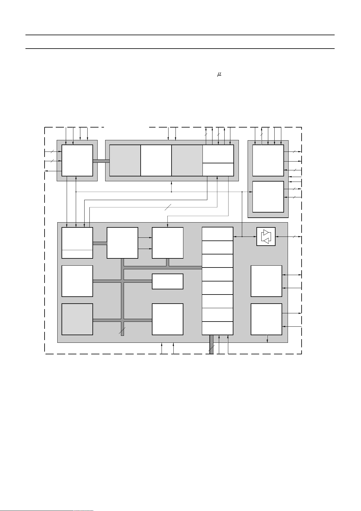
4-1-1 Block diagr am off the VCT ................................................................................................................... 18
4-1-2 TV -signal Processor ........................................................................................................................... 18
4-1-2 -Controller
......................................................................................................
.
...................................
1
9
4-1-4 Teletext Features ................................................................................................................................ 19
4-1-5 Displaty OSD F eatures...................................................................................................................... 20
4-1-6 Audio Features ................................................................................................................................... 20
4-1-7 General Features ............................................................................................................................... 20
4-1-8 Data Capture ....................................................................................................................................... 20
4-1-9 Data Capture Features ........................................................................................................................ 20
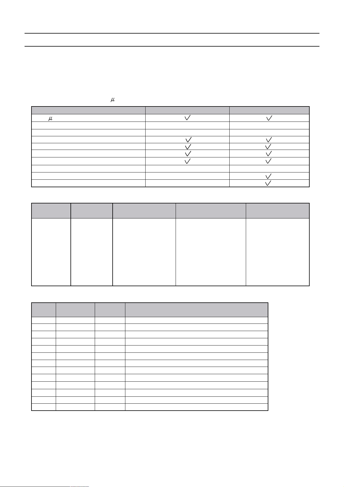
4-1-10 TV processor version and -Controller capacity .............................................................................. 21
4-1-11 IC marking and version ....................................................................................................................... 21
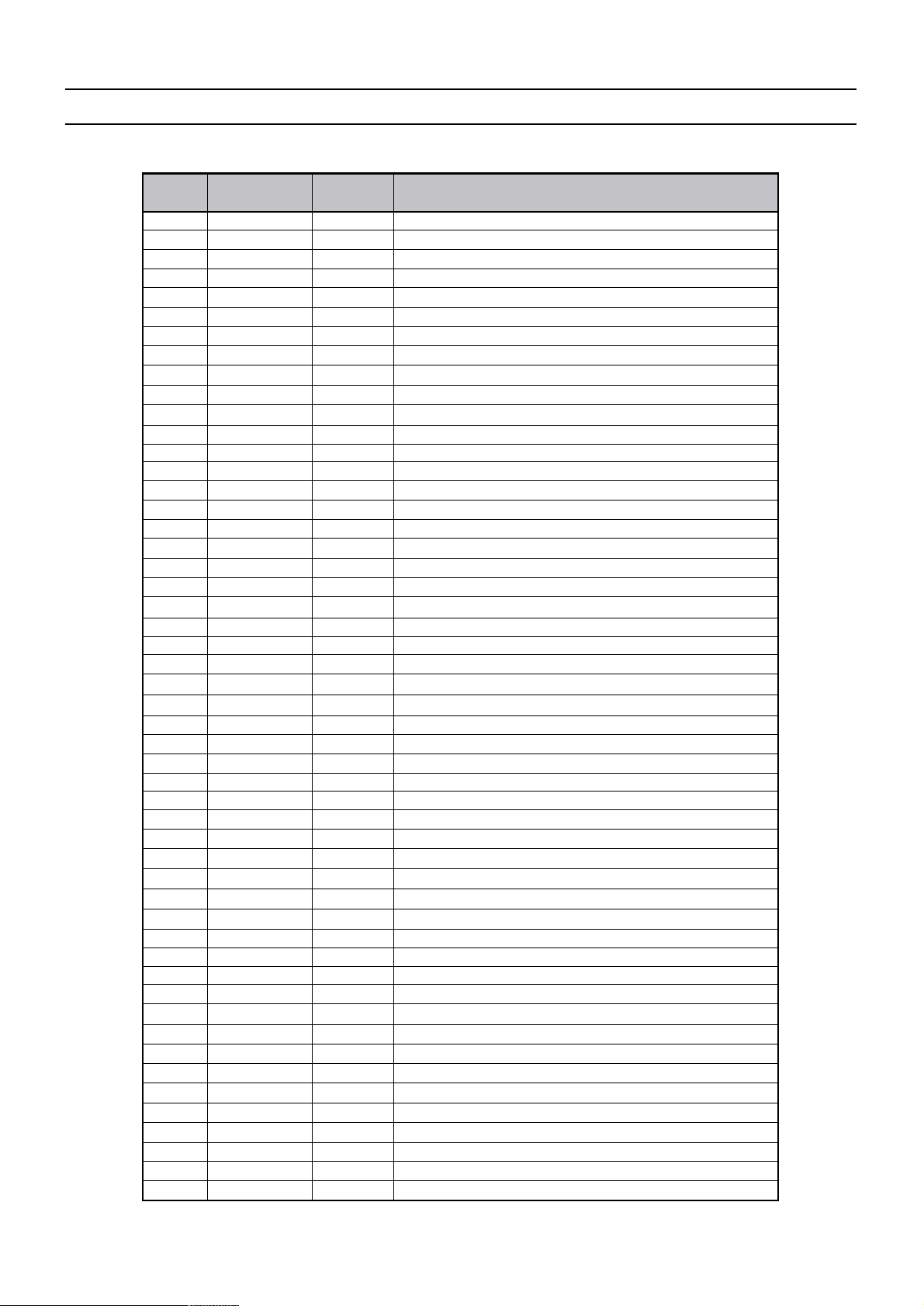
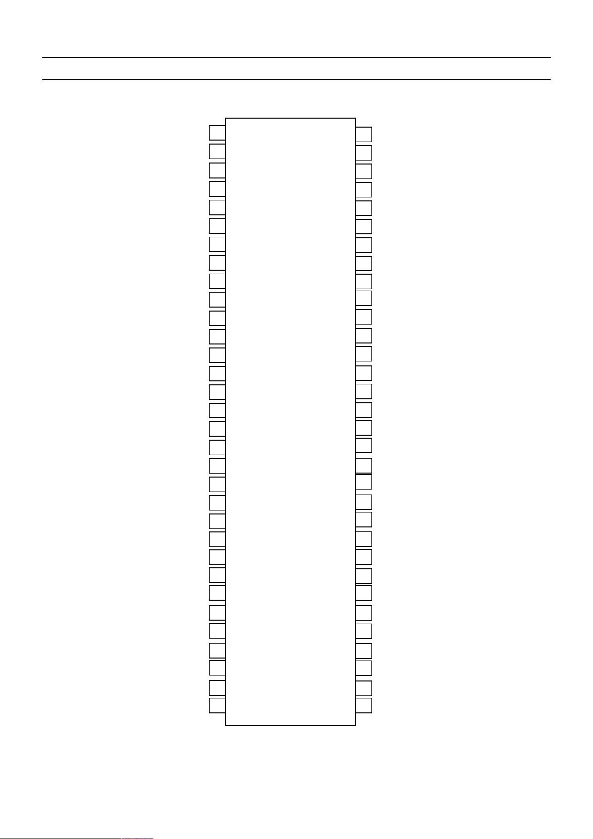
4-1-12 Pinning ................................................................................................................................................ 21
4-2 MSP341x Multistandard Sound Processor ................................................................................................... 24
4-2-1 Basic F eatures of the MSP 341x ......................................................................................................... 24
4-3 TDA4470 - Multistandard Video-IF and Quasi P arallel Sound Processor ...................................................... 28
4-3-1 Description .......................................................................................................................................... 28
4-3-2 Features .............................................................................................................................................. 28
4-3-3 Pinning ................................................................................................................................................ 28
4-3-4 Block diagram .................................................................................................................................... 29
4-4 T D A894xJ Stereo A udio Amplifier ........................................................................................ ......................... 30
4-4-1 Features ............................................................................................................................................... 30
4-5 TDA835xJ Vertical Amplifier ........................................................................................................................... 32
4-5-1 TDA8357J ........................................................................................................................................... 32
Page 3

Service manual SC-150
-2-
4-5-2 TDA8358J ..............................................................................................................................................33
4-6 TDA6107Q.......................................................................................................................................................... 33
4-7 24C16 - 16 Kb EEPROM .................................................................................................................................... 35
4-8 STR - F6653....................................................................................................................................................... 36
4-8-1 General description ............................................................................................................................... 36
4-8-2 Features................................................................................................................................................. 36
4-8-3 Block diagram .......................................................................................................................................36
4-8-4 Pin description ...................................................................................................................................... 37
4-8-5 Control part - electrical characteristics ................................................................................................. 37
4-8-6 MOSFET electrical characteristics .......................................................................................................38
4-9 CXA1315P
4-10 CXA1315P
......................................................................................................................................................... 39
4-9-1 General description................................................................................................................................ 39
4-9-2 Features ................................................................................................................................................39
4-9-3 Block diagram ........................................................................................................................................
4-9-4 Pin Description........................................................................................................................................
39
40
..........................................................................................................................................................
40
4-10-1 General description................................................................................................................................
40
4-10-2 Features ................................................................................................................................................
40
4-10-3 Block diagram ........................................................................................................................................
40
4-10-4 Pin Description........................................................................................................................................
40
4-11 LA6515
..........................................................................................................................................................
40
4-11-1 General description................................................................................................................................
40
4-11-2 Features ................................................................................................................................................
40
4-11-3 Block diagram ........................................................................................................................................
40
4-11-4 Pin Description........................................................................................................................................
40
5 - Circuit description..................................................................................................................................................
5-1 Block diagram....................................................................................................................................................43
43
5-2 IF section............................................................................................................................................................44
5-2-1 Block diagram .......................................................................................................................................44
5-2-2 Vision IF Amplifier .................................................................................................................................. 44
5-2-3 Tuner-and VIF-ACG ................................................................................................................................ 45
5-2-4 FPLL, VCO and AFC.............................................................................................................................. 45
5-2-5 Video Demodulation and Amplifier ...................................................................................................... 46
5-5-6 Sound IF Amplifier and SIF-AGC ....................................................................................................... 46
5-2-7 Quasi-Parallel-Sound (QPS) Mix er ......................................................................................................... 46
5-2-8 Standard Switch .................................................................................................................................... 46
5-2-9 L Switch.................................................................................................................................................. 46
5-2-10 Internal Voltage Stabiliser ..................................................................................................................... 46
5-3 Video - VCT description ......................................................................................................................................47
5-3-1 Introduction ............................................................................................................................................47
5-3-2 Video Front-end..................................................................................................................................... 47
5-3-3 Input Selector........................................................................................................................................ 47
5-3-4 Clamping ................................................................................................................................................47
5-3-5 A utomatic Gain Control ........................................................................................................................ 47
5-3-6 Digitally Controlled Clock Oscillator..................................................................................................... 47
5-3-7 Analogue Video Output ........................................................................................................................ 47
5-3-8 Adaptiv e Comb Filter (VCT3834A only)................................................................................................ 48
5-3-9 Color Decoder ....................................................................................................................................... 48
5-3-10 Horizontal Scaler ................................................................................................................................... 48
5-3-11 Video Sync Processing ........................................................................................................................ 49
5-3-12 Display Processing................................................................................................................................ 49
5-3-13 Chroma Transient Improvement............................................................................................................ 49
5-3-14 Video Back-end ..................................................................................................................................... 49
5-3-15 CRT Measurement and Control........................................................................................................... 50
5-3-16 Average Beam Current Limiter ............................................................................................................. 50
Page 4

Service manual SC-150
-3-
Fo
5-4-1 Introduction........................................................................................................................................... 51
5-4-2 CPU ...................................................................................................................................................... 51
............................................................................... 52
5-4-4 Tuning .................................................................................................................................................. 52
5-4-5 Automatic rmat switching and WSS ...................................................................................... ......... 52
5-4-6 EXTERNAL source control logic........................................................................................................... 54
5-4-7 Over Current Protection........................................................................................................................ 55
5-5Teletext Display................................................................................................................................................. 55
5-6 Sound processing............................................................................................................................................... 56
5-6-1 Analogue sound IF-input section............................................................................................................ 56
5-6-2 Quadrature Mixers................................................................................................................................ 56
5-6-3 Phase and AM discr imination........................................................................................................... 56
5-6-4 NICAM decoder.................................................................................................................................... 57
5-6-5 DSP section.......................................................................................................................................... 57
5-6-6 Sound Mode switching.......................................................................................................................... 57
5-7 Sound amplification........................................................................................................................................... 57
5-7-1 Power amplifier..................................................................................................................................... 57
5-7-2 Mode selection....................................................................................................................................... 58
5- 8 Vertical deflection............................................................................................................................................. 58
5-8-1 Flyback voltage..................................................................................................................................... 58
5-8-2 Protection.............................................................................................................................................. 58
5-8-3 Guard circuit.......................................................................................................................................... 58
5-8-4 Damping resistor................................................................................................................................... 58
5-8-5 EAST-WEST Amplifier (TDA8358J only)............................................................................................... 58
5-9 Power supply (STR F6653).. .............................................................................................................................. 59
5-9-1 STR-F6654 generaral description......................................................................................................... 59
5-9-2 Power supply primary part operations................................................................................................... 59
5-10TV start-up ,TV normal run and stand by mode operations............................................................................... 63
5-10-1 TV start-up operations.......................................................................................................................... 63
5-10-2 TV normal r un and stand-by mode operations....................................................................................... 64
6 - Se
6 -1 Service part list
rvice parts list.. ......................................................................................................... .......................................
...........................................................................................................................................
.
69
69
6 -2 Service part list option
...............................................................................................................................
79
7 - Exploded Vie w
........................................................................................................................................................
80
..............................................................................................................
..........................................
81
..............................................................................................................
..........................................
83
8 - PCB Layout
.........................................................................................................
..........................................
81
8 -1 MAIN PCB
.........................................................................................................
..........................................
82
8 -2 UNION PCB
9 - Circuit Diagram
..........................................................................................
..........................................
83
9 - 1 Circuit Diagram(MAIN)
........................................................................................
..........................................
84
9 - 2 Circuit Diagram
(UNION)
5-4-3
-Controller I/O pin configuration and function
5-3-17 Analogue RGB Insertion .....................................................................................................................50
5-3-18 Fast-Blank Monitor ................................................................................................................................ 50
5-3-19 Vertical and East/West Deflection ....................................................................................................... 50
5-3-20 EHT Compensation ................................................................................................................................ 51
5-3-21 Reset Function ...................................................................................................................................... 51
5-3-22 Standby and Pow er-On ........................................................................................................................51
5-4 Micro-controller......................................................................................................................................................... 51
Page 5
Service manual SC-150
-4-
1- Main Featur e s
1-1 Specifications
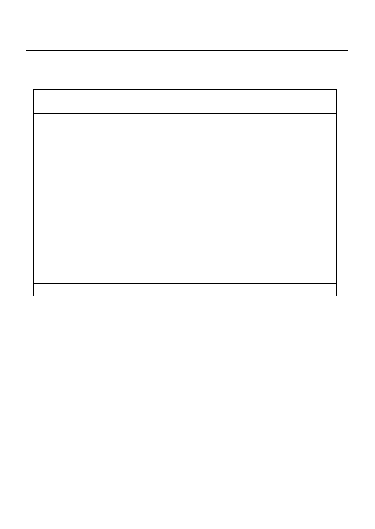
TV standard PAL - SECAM B/G D/K, PAL I/I, SECAM L/L'
Sound system NICAM B/G, I, D/K, L,
FM 2Carrier B/G, D/K
Power consumption
Sound Output Pow
er
7W x2 (at 1KHz, 60% mod, 10% THD)
Speaker
10W(Normal) 8 ohm X 2
Teletext system
10 pages memory FASTEXT (FLOF or TOP)
Aerial input
75 ohm unbalanced
Channel coverage
Off-air channels, S-cable channels and hyperband
Tuning system
frequency synthesiser tuning system
V
isual screen
32" : 76Cm
Channel indication On Screen Display
program Selection 100 programmes
Aux. terminal
Remote Control Unit R-46G22
32" 16:9 Real Flat : 110W approx.
EURO-SCART 1 : Audio / Video In and Out, R/G/B In, Slow and
Fast switching.
EURO-SCART 2 : Audio / Video In and Out, SVHS In.
AV3 : Audio-Video Jack on right side of cabinet.
Headphone jack (3.5 mm) on right side of cabinet
SVHS3 : Jack on right side of cabinet - sound input
common wit
h AV3.
Monitor Out
Page 6
Service manual SC-150
-5-
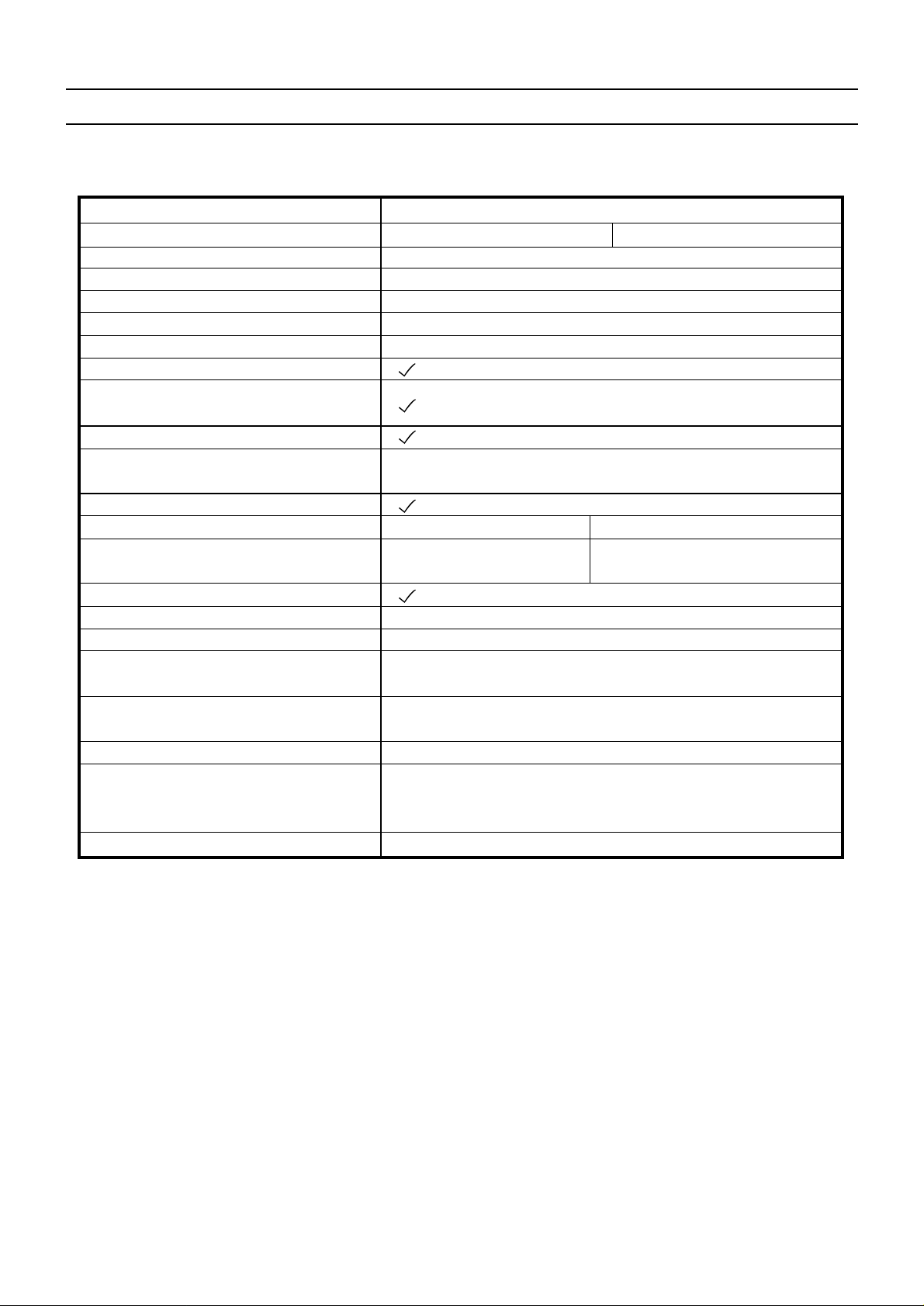
Specification matrix
Chassis Name
3834
A
R46G22
4859812224(MAIN)/ 4959812324(Union)
16:9 Real Flat
Auto / 4:3 / 14:9 / Zoom 14:9 /Zoom
16:9 / Full Screen
3410G
Off / Spatial
Dedicated
10 Page
Available : Selectable in factory /
Service mode by option bits
Available : Selectable in factory /
Service mode by option bits
"Pan-European Latin, Cyrillic, Greek"
"English, French, German, Italian, Spanish,Dutch, Danish,
Finnish, Norwegian, Swedish, Greek,Polish, Czech, Slovakian,
Romanian, Russian, Bulgarian, Hungarian
"Philips, Alps,Partsnic"
3411G
Off / Spatial / Panorama /
Dolby Virtual
SC-150
VCT Version
Software Version
Remote Control
PCB Serial Number
Tube
SVHS 3
"Picture Improvements,
Comb Filter, Horizontal Scaler"
Teletext Split Screen
Formats Available in Video Mode
AV2 Monitor Output
MSP Version
Sound Dffects
Graphic Equalizer
AV3 Audio Input
Teletext Page Memory
Top Teletext
Flof Teletext
Text Character Support
OSD Languages
Tuner Options
Model Name
DSC-3220E DSC-3220L
Page 7
Service manual SC-150
-6-
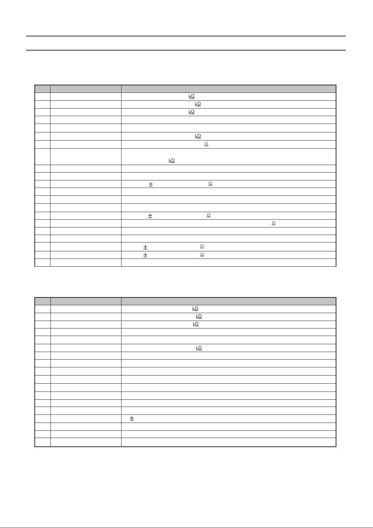
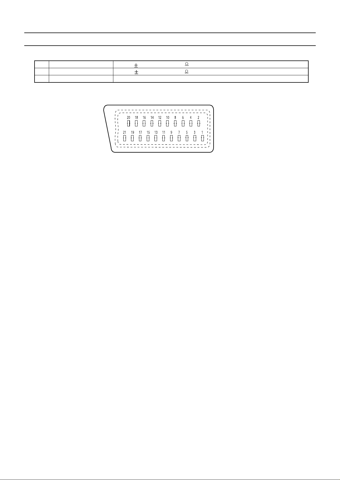
21 Pin EURO-SCART 1 :
Pin Signal Description Matching value
1 Audio Output Right 0.5 Vrms, Impedance < 1 , ( RF 54% Mod )
2 Audio Input Right 0.5 Vrms, Impedance > 10
3 Audio Output Left 0.5 Vrms, Impedance < 1 , ( RF 54% Mod )
4 Audio Earth
5 Blue Earth
6 Audio Input Left 0.5 Vrms, Impedance > 10
7 Blue Input 0.7 Vpp ±0.1V, Impedance 75
8 Slow Switching TV : 0 to 2V, AV 16/9 : 4.5 to 7V, AV 4/3 : 9.5 to 12V ,
Impedance > 10
9 Green Earth
10 N.C.
11 Green Input 0.7 Vpp 0.1V, Impedance 75
12 N.C.
13 Red Earth
14 Blanking Earth
15 Red Input 0.7 Vpp 0.1V, Impedance 75
16 Fast Switching 0 to 0.4V : Logic “0”, 1 to 3V : Logic “1”, Impedance 75
17 Video Out Earth
18 Video In Earth
19 Video Output 1 Vpp 3dB, Impedance 75
20 Video Input 1 Vpp 3dB, Impedance 75
21 Common Earth
21 Pin EURO-SCART 2 :
Pin Signal Description Matching value
1 Audio Output Right 0.5 Vrms, Impedance < 1 , ( RF 54% Mod ) - Not available for cp885
2 Audio Input Right 0.5 Vrms, Impedance > 10
3 Audio Output Left 0.5 Vrms, Impedance < 1 , ( RF 54% Mod ) - Not available for cp885
4 Audio Earth
5 Earth
6 Audio Input Left 0.5 Vrms, Impedance > 10
7 N.C.
8 Slow Switching TV: 0 to 2V, AV 16:9: 4.5V to 7V, AV 4:3: 9.5 to 12V
9 N.C.
10 N.C.
11 N.C.
12 N.C.
13 Earth
14 Earth
15 Chroma Input 3dB for a luminance signal of 1 Vpp
16 N.C.
17 Earth
18 Video In Earth
Page 8
Service manual SC-150
-7-
19 Video Output 1 Vpp 3dB, Impedance 75 ( Monitor output ) - Not available for cp885
20 Video Input, Y In. 1 Vpp 3dB, Impedance 75
21 Common Earth
Page 9
Service manual SC-150
-8-
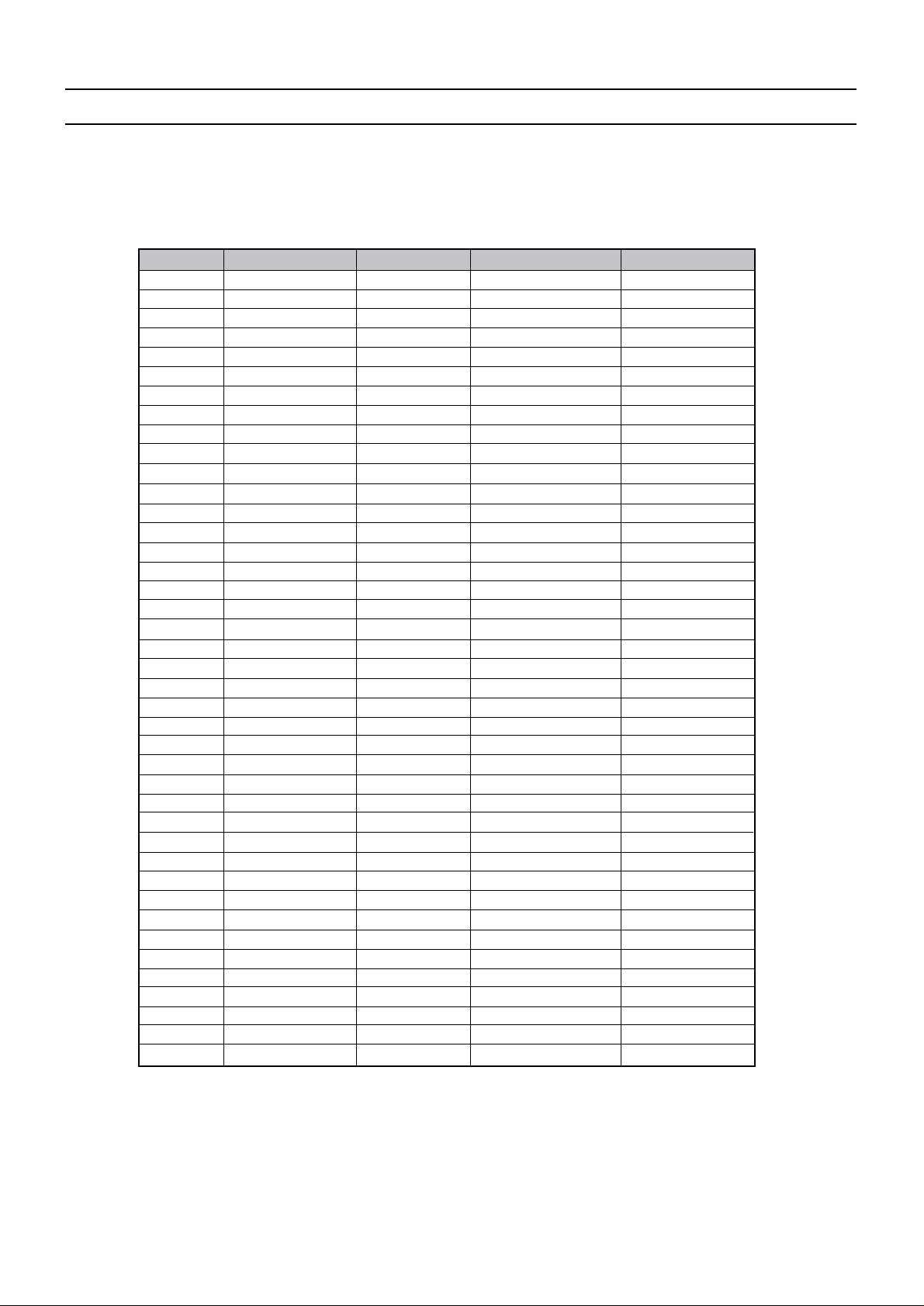
CH EUROPE CCIR FRANCE GB(IRELAND) EAST OIRT
C01 46.25 - 47.75 49.75
C02 48.25 55.75 (L’) 53.75 59.25
C03 55.25 60.5 (L’) 61.75 77.25
C04 62.25 63.75 (L’) 175.25 85.25
C05 175.25 176.00 183.25 93.25
C06 182.25 184.00 191.25 175.25
C07 189.25 192.00 199.25 183.25
C08 196.25 200.00 207.25 191.25
C09 203.25 208.00 215.25 199.25
C10 210.25 216.00 223.25 207.25
C11 217.25 189.25 (LUX) 231.25 215.25
C12 224.25 69.25 (L’) 239.25 223.25
C13 53.75 76.25 (L’) 247.25 -
C14 - 83.25 (L’) 49.75 -
C15 82.25 90.25 57.75 C16 - 97.25 65.75 C17 183.75 - 77.75 C18 192.25 - 85.75 C19 201.25 - - C20 -- - C21 471.25 471.25 471.25 471.25
C22 479.25 479.25 479.25 479.25
C23 487.25 487.25 487.25 487.25
C24 495.25 495.25 495.25 495.25
C25 503.25 503.25 503.25 503.25
C26 511.25 511.25 511.25 511.25
C27 519.25 519.25 519.25 519.25
C28 527.25 527.25 527.25 527.25
C29 535.25 535.25 535.25 535.25
C30 543.25 543.25 543.25 543.25
C31 551.25 551.25 551.25 551.25
C32 559.25 559.25 559.25 559.25
C33 567.25 567.25 567.25 567.25
C34 575.25 575.25 575.25 575.25
C35 583.25 583.25 583.25 583.25
C36 591.25 591.25 591.25 591.25
C37 599.25 599.25 599.25 599.25
C38 607.25 607.25 607.25 607.25
C39 615.25 615.25 615.25 615.25
C40 623.25 623.25 623.25 623.25
C41 631.25 631.25 631.25 631.25
1-2 Channel table
FREQUENCY TABLE
Page 10
Service manual SC-150
-9-
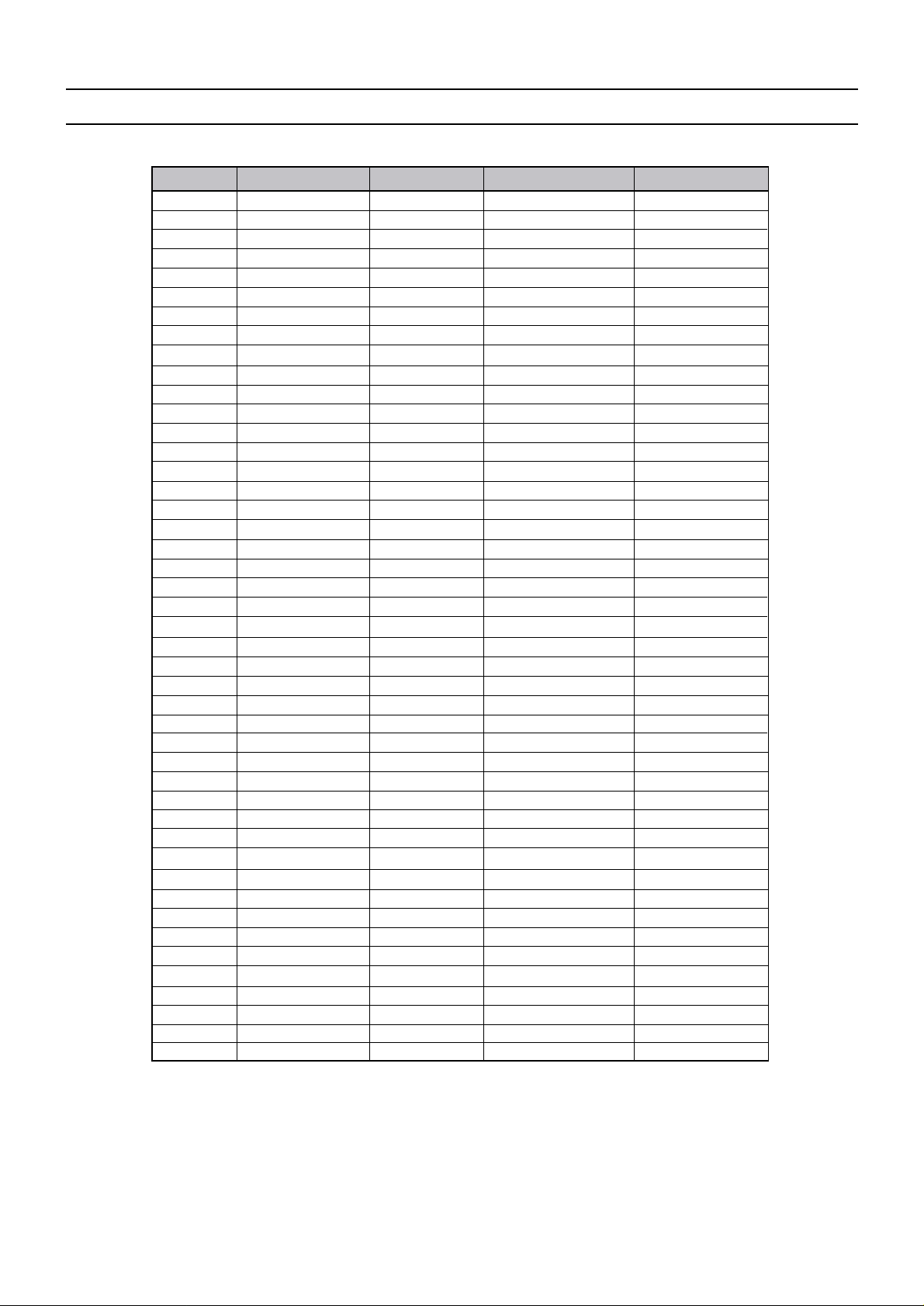
CH EUROPE CCIR FRANCE GB(IRELAND) EAST OIRT
C42 639.25 639.25 639.25 639.25
C43 647.25 647.25 647.25 647.25
C44 655.25 655.25 655.25 655.25
C45 663.25 663.25 663.25 663.25
C46 671.25 671.25 671.25 671.25
C47 679.25 679.25 679.25 679.25
C48 687.25 687.25 687.25 687.25
C49 695.25 695.25 695.25 695.25
C50 703.25 703.25 703.25 703.25
C51 711.25 711.25 711.25 711.25
C52 719.25 719.25 719.25 719.25
C53 727.25 727.25 727.25 727.25
C54 735.25 735.25 735.25 735.25
C55 743.25 743.25 743.25 743.25
C56 751.25 751.25 751.25 751.25
C57 759.25 759.25 759.25 759.25
C58 767.25 767.25 767.25 767.25
C59 775.25 775.25 775.25 775.25
C60 783.25 783.25 783.25 783.25
C61 791.25 791.25 791.25 791.25
C62 799.25 799.25 799.25 799.25
C63 807.25 807.25 807.25 807.25
C64 815.25 815.25 815.25 815.25
C65 823.25 823.25 823.25 823.25
C66 831.25 831.25 831.25 831.25
C67 839.25 839.25 839.25 839.25
C68 847.25 847.25 847.25 847.25
C69 855.25 855.25 855.25 855.25
C70 863.25 863.25 863.25 863.25
C71 69.25 - - -
C72 76.25 - - -
C73 83.25 - - -
C74 90.25 - - -
C75 97.25 - - -
C76 59.25 - - -
C77 93.25 - - -
S01 105.25 104.75 103.25 105.25
S02 112.25 116.75 111.25 112.25
S03 119.25 128.75 119.25 119.25
S04 126.25 140.75 127.25 126.25
S05 133.25 152.75 135.25 133.25
S06 140.25 164.75 143.25 140.25
S07 147.25 176.75 151.25 147.25
S08 154.25 188.75 159.25 154.25
S09 161.25 200.75 167.25 161.25
Page 11
Service manual SC-150
-10-
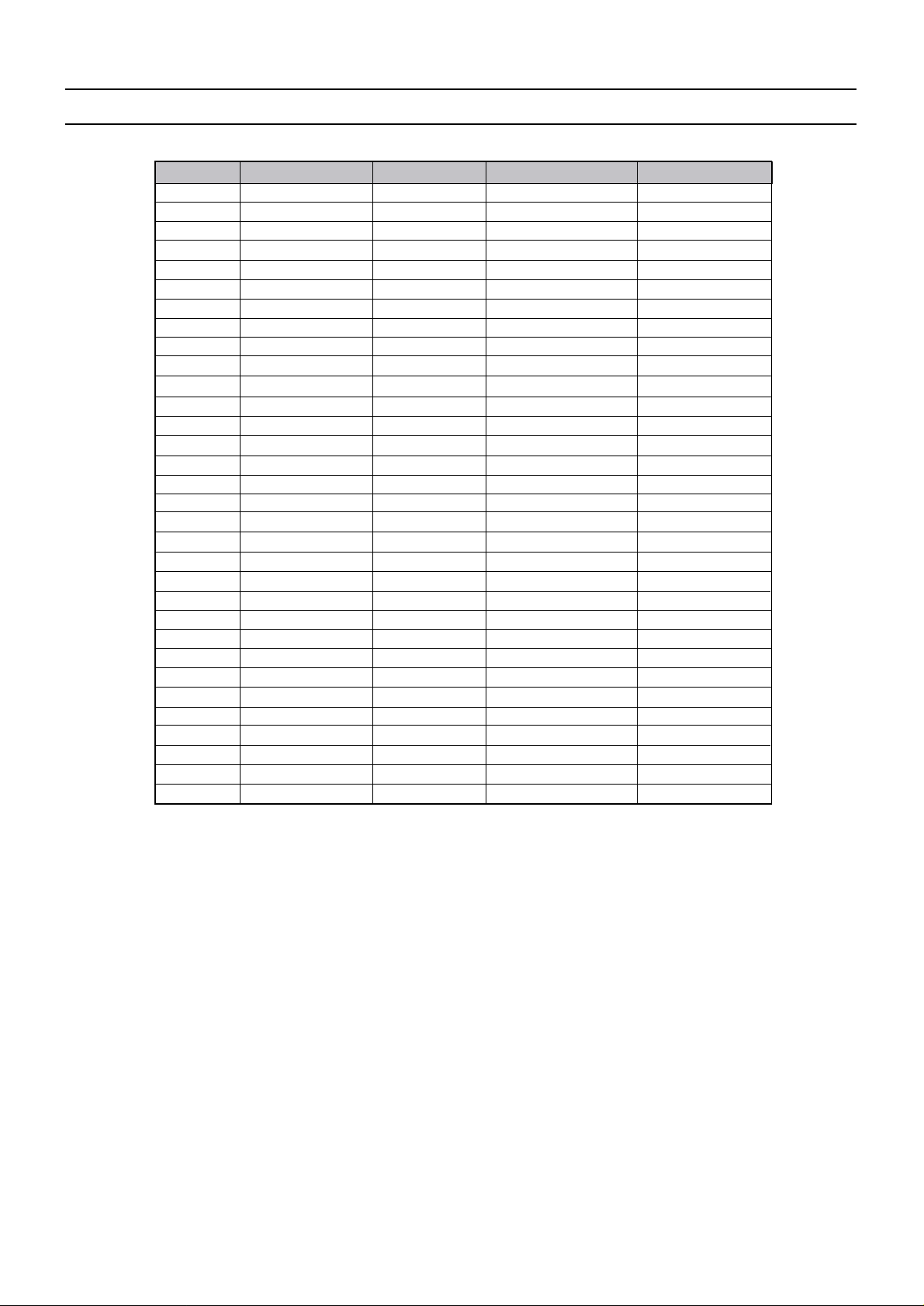
CH EUROPE CCIR FRANCE GB(IRELAND) EAST OIRT
S10 168.25 212.75 - 168.25
S11 231.25 224.75 - 231.25
S12 238.25 236.75 - 238.25
S13 245.25 248.75 255.25 245.25
S14 252.25 260.75 263.25 252.25
S15 259.25 272.75 271.25 259.25
S16 266.25 284.75 279.25 266.25
S17 273.25 296.75 287.25 273.25
S18 280.25 136.00 295.25 280.25
S19 287.25 160.00 303.25 287.25
S20 294.25 - - 294.25
S21 303.25 303.25 - 303.25
S22 311.25 311.25 311.25 311.25
S23 319.25 319.25 319.25 319.25
S24 327.25 327.25 327.25 327.25
S25 335.25 335.25 335.25 335.25
S26 343.25 343.25 343.25 343.25
S27 351.25 351.25 351.25 351.25
S28 359.25 359.25 359.25 359.25
S29 367.25 367.25 367.25 367.25
S30 375.25 375.25 375.25 375.25
S31 383.25 383.25 383.25 383.25
S32 391.25 391.25 391.25 391.25
S33 399.25 399.25 399.25 399.25
S34 407.25 407.25 407.25 407.25
S35 415.25 415.25 415.25 415.25
S36 423.25 423.25 423.25 423.25
S37 431.25 431.25 431.25 431.25
S38 439.25 439.25 439.25 439.25
S39 447.25 447.25 447.25 447.25
S40 455.25 455.25 455.25 455.25
S41 463.25 463.25 463.25 463.25
Page 12
Service manual SC-150
-11-
1-3 ATSS sorting method
The TV set sweeps all the TV bands from beginning of VHF to end of UHF. The TV controlling software for each
pro gram checks if a VPS CNI code is transmitted ( this system exists for German, Swiss and Austrian transmissions).
If no VPS CNI code is found, then the system check if a CNI code is transmitted as part of the teletext transmission
( Packet 8/30 format 1 ). If such a code ( VPS or teletext ) is found and if this code is in the ATSS list, the program is
automatically named.
If the transmission does not have VPS CNI, and no teletext service is availab le, then there is no possibility of the
program being automatically named.
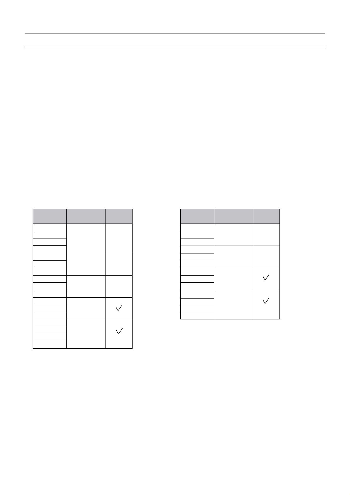
The programs found are then sorted in 4 groups :
Group I : It contains all the pro grams from the selected country and named by the TV controlling software. Within this
group the sorting order is fixed by the ATSS list.
Group II : It contains all the pro grams with a strong signal strength which are not listed in group I.
Group III : It contains all the pro grams with a weak signal strength which are not listed in group I.
Group IV : If two or more progr ams with the same code are found, only the strongest ( or if they have the same level
the one with the lowest frequency) is listed in group I, II or III. The others are listed in group IV.
Program
number
1
2 Group I
...
n
n+1
... Group II
m
m+1
... Group III
p
p+1
... Group IV
q
q+1
.... not used
99
0
Group
Skip
Program
number
1
... Group II
m
m+1
... Group III
p
p+1
... Group IV
q
q+1
.... not used
99
0
Group
Skip
Special case : Country selection = Others
Special case : France
Note : If two programs with the same name but a different code ar e found these two programs are listed in
gr oup I, II or III ( e.g. Regional program SW3 in Germany ).
Page 13

Service manual SC-150
-12-
The sor ting order within group II, III, and IV is based on the channel frequency. The Pro gram with the lo west
frequency is allocated the first rank in its group, and so f orth until the last program of the group which has the
highest fr equency.
If France is selected, the TV controlling soft w are first swe eps all TV bands with Fr ance system selected
( positive video modulation) and the a second time with Europe system selected ( neg ative video modulation).
Special case : Switzerland
If Switzerland is selected th e TV controlling softw are f irst s weeps all TV bands with Eur ope system selected
(neg ative video modulation) and then a second time with France system selected ( positi ve video modulation).
Special case : GB
Note for sa tellite recei ver users : Before starting ATSS tur n On your satellite r eceiver and tune “ SKY NEWS ”.
If GB is selected the TV controlling software seeks for programs only in UHF ( C21 to C70 ).
The sorting order is :
1 - BBC1
2 - BBC2
3 - ITV
4 - CH4
5 - CH5
6 - NEWS
If two or more “ identical” pr ograms ( same name but diffe rent code e.g. BBC1 and BBC1 Scotland ) are found
the following pro grams in the list will be shifted up. (1 - BBC1, 2 - BBC1, 3 - BBC2, 4 -ITV, 5 - CH4, 6 - CH5,
7 - NEWS, ..)
If one of the progr am abo ve is not f ound, the associated program number remains empty
( freq.=467.25 Mhz - Skip selected - no name - system=GB).
example A : 1 - BBC1, 2 - BBC2, 3 - ITV , 4 - ----, 5 - CH5, 6 - NEWS , ...
example B ( if 2 BBC1 found ) : 1 - BBC1, 2 - BBC1, 3 - BBC2, 4 - IT V, 5 - -----, 6 - CH5, 7 -NEWS, ...
Special case : France
Page 14

Service manual SC-150
-13-
2 - Safety instruction
WARNING: Only competent service personnel may carry out work involving the testing or repair of this equipment.
X-RAY RADIATION PRECAUTION
1. Excessive high voltage can produce potentially hazardous X-RAY RADIATION. To avoid such hazards, the high
voltage must not exceed the specified limit. The nominal value of the high voltage of this receiver is
26 KV (25” - 28”) at max beam current. The high voltage must not, under any circumstances,
exceed 29.5 KV (25") or
30 KV (28"). Each time a receiver requires servicing, the high voltage should be checked.
It is important to use an accurate and reliable high voltage meter.
2. The only source of X-RAY Radiation in this TV receiver is the picture tube. For continued X-RAY RADIATION
protection, the replacement tube must be exactly the same type tube as specified in the parts list.
SAFETY PRECAUTION
1. Potentials of high voltage are present when this receiver is operating. Operation of the receiver outside the cabinet
or with the back board removed involves a shock hazard from the receiver.
1) Servicing should not be attempted by anyone who is not thoroughly familiar with the precautions necessary
when working on high voltage equipment.
2) Discharge the high potential of the picture tube before handling the tube. The picture tube is highly evacuated
and if broken, glass fragments will be violently expelled.
2. If any Fuse in this TV receiver is blown, replace it with the FUSE specified in the Replacement Parts List.
3. When replacing a high wattage resistor ( metal oxide film resistor) in the circuit board, keep the resistor
10 mm away from circuit board.
4. Keep wires away from high voltage or high temperature components.
5. This receiver must operate under AC 230 volts, 5O Hz. NEVER connect to DC supply or any other power or
frequency.
PRODUCT SAFETY NOTICE
Many electrical and mechanical parts in this equipment have special safety-related characteristics.
These characteristics are often passed unnoticed by a visual inspection and the X-RAY RADIATION protection
afforded by them cannot necessarily be obtained by using replacement components rated for higher voltage,
wattage, etc. Replacement parts which have these special safety characteristics are identified in this manual and its
supplements, electrical components having such features are identified by designated symbol on the parts list.
Before replacing any of these components, read the parts list in this manual carefully. The use of substitutes
replacement parts which do not have the same safety characteristics as specified in the parts list may create X-RAY
Radiation.
Page 15
Service manual SC-150
-14-
3 - Alignment instructions
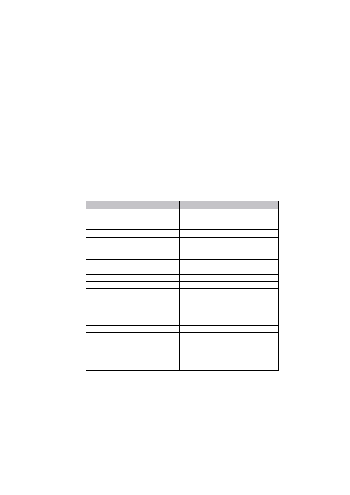
3-1 Microcontroller configuration : Service mode
To switch the TV set into service mode please see instruction below.
1 - Select pr. number 91
2 - Adjust sharpness to minimum and exit all menu.
3 - Quickly press the key sequence : RED - GREEN - menu
To software version is displ ayed beside the word Service, e.g. “ SERVICE V2.00A”.
To exit SERVICE menu press menu key or Std By key.
3-2 Service mode na vigation
Pr Up / Down remote keys : cycle through the service items available.
Vol- / + remote keys : Decrement / Increment the value s within rang e.
0~7 digit keys : Toggle bits 0~7 in option byte
Order Item
Default settingh for SC-150
1 PARABOLA
+124
2 HOR WIDTH
-1350
3 CORNER
-97
4 HOR.PARAL
-1
5 V.LINEAR
0
6 EW TRAPEZ
-30
7 S CORRECT
-21
8 H BOW
+100
9 VERT SIZE
+157
10 VERT CENT
+3889
11 RED GAIN
+97
12 GRN GAIN
+87
13 BLUE GAIN
+95
14 RED BIAS
+128
15 GRN BIAS
+128
16 HOR CEN
92
17 AGC LEVEL
-
18 G2-SCREEN
-
19 AFT
-
20 OPTION1
OPTION2
-
-
21
22 MAX VOL
Not used
Page 16
Service manual SC-150
-15-
3-3 Microcontroller configuration : Option bits
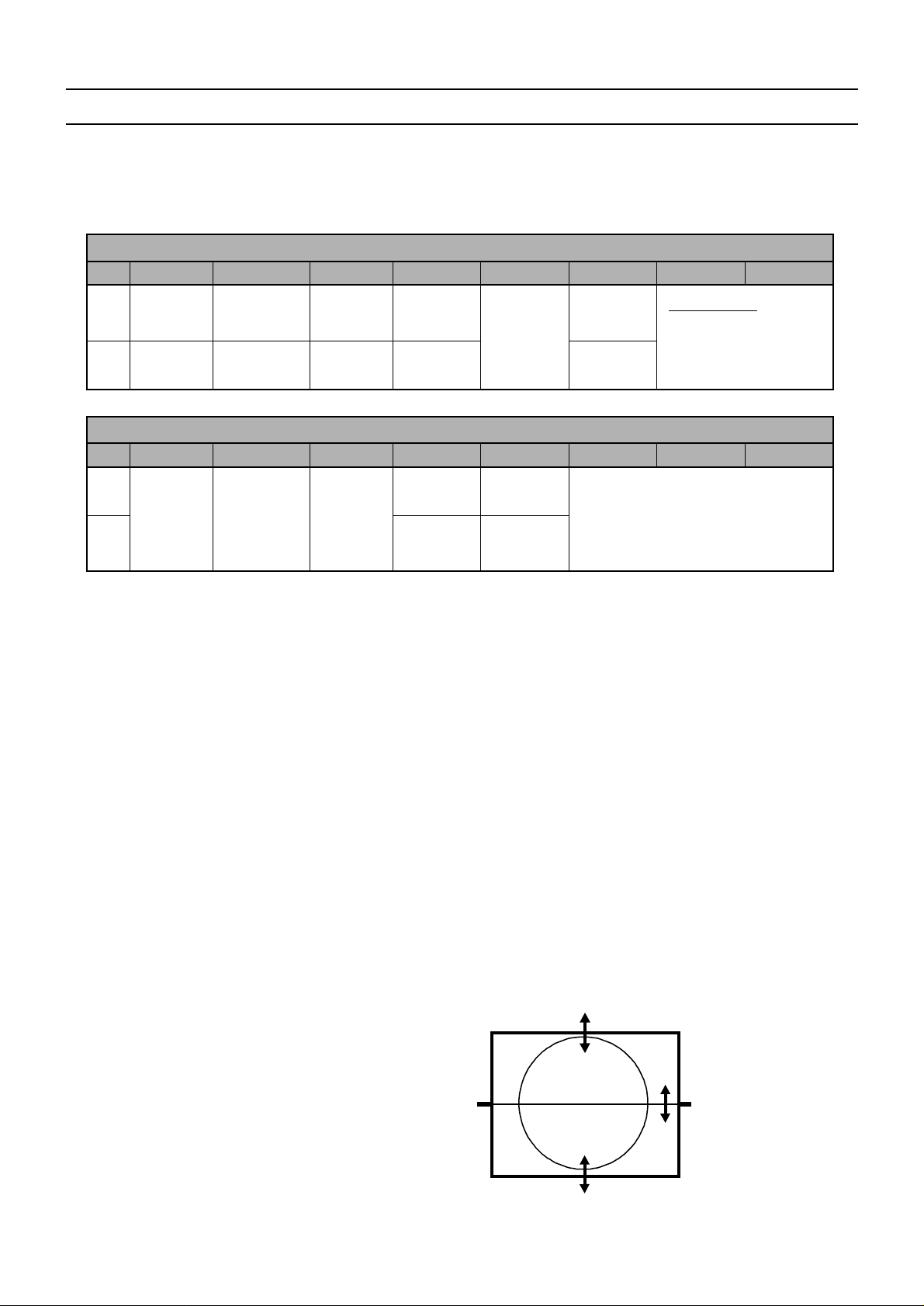
These option bits are available from Service mode. First find the OPTION contr ol, and then use keys 0...7 on the
remote ke ypad to control bits 0 to 7 respectively. The table below shows the options a vailable ;
1
0
B7 B6
TOP text
off
FASTEXT
FLOF off
TOP text
on
FASTEXT
(FLOF) on
B5 B4 B3 B2 B1 B0
TUBE 4:3
AUTO 4:3
switch to
PANORAMA
TUBE 16:9
AUTO 4:3
switch to 4:3
SVHS3
disable
00=Philips
01=ALPS
10=Philips (AGC intern)
11=DAEWOO
SVHS3
enable
X
Set all the unused bits, markde 'X', to be 0 for future compatibility.
3-4 TV set Alignment
3-4-1- Local oscillator alignment
Tune a colour bar pattern. The Frequency of the signal carrier must be accurate (Max +/- 10khz deviation fron the
nominal channel frequency).
Find "AFT" item in service mode.
Adjust the coil L150 to bring the cursor to central position : 32.
3-4-2- G2 alignment
- Tune a colour bar pattern.
- Find the "G2 - SCREEN" item in service mode.
- Adjust screen volume (on FBT) to bring the cursor to central position : 32.
3-4-3- White balance
- Select a dark picture and adjust RED BIAS and GRN BIAS to the desired colour temperature.
- Select a bright picture and adjust REC, GRN and BLUE GAIN to the desired dolour temperature.
3-4-4- Forcus
Adjust the Forcus volume (on FBT) to have the best resolution on screen.
3-4-5- Vertical geometry
Adjust V.LINEAR (linearity), S CORRECT
(S. Corrention), VERT SIZE (Vertical amplitude),
VERT CENT (vertical centing) to compensate
for vertical distortion.
OPTION 1
1
0
B7 B6
Y
Y
B5 B4 B3 B2 B1 B0
PICTURE
TILT on
Y
PICTURE
TILT off
See table below.
OPTION 2 bits B2 B1 B0
Normal I
brightness
Normal I
brightness
+5 steps
OPTION 2
Tuner options
Page 17
Service manual SC-150
-16-
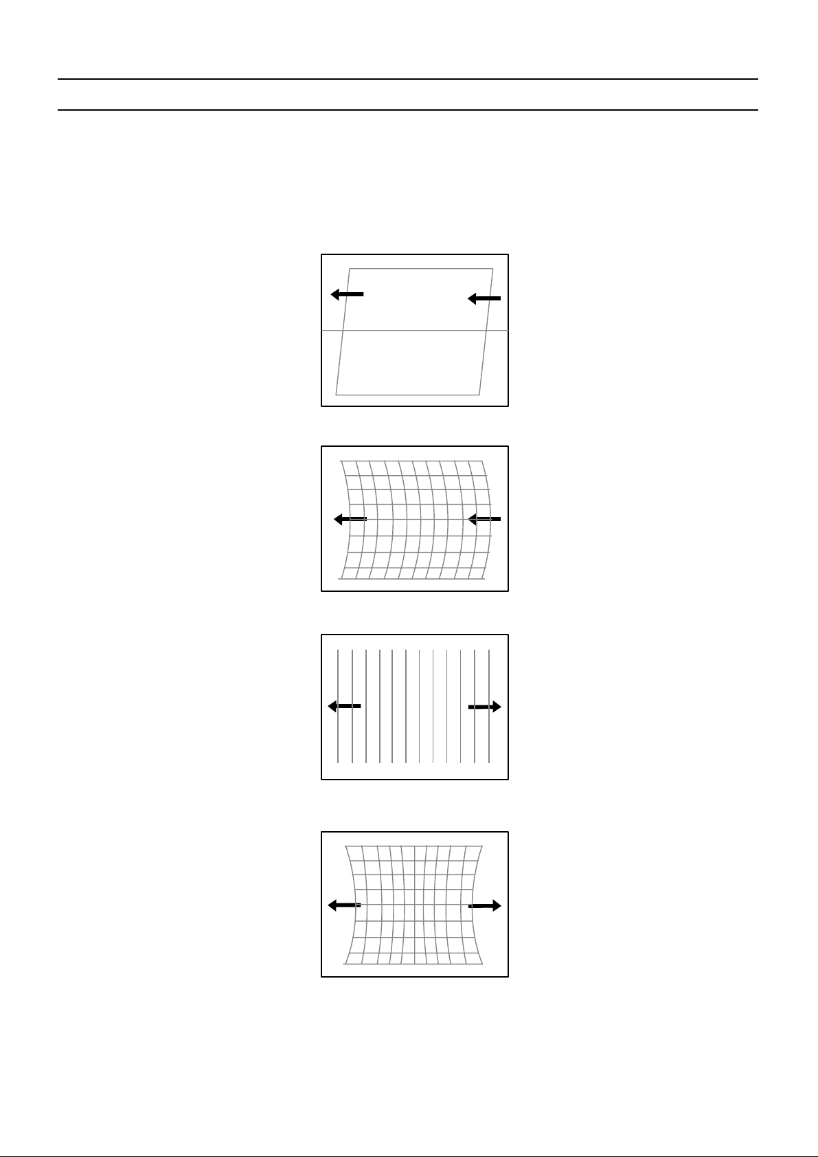
HOR PARAL
H BOW
HOR WIDTH
PARAROLA
3-4-6- Horizontal picture centring
Adjust HOR CEN(Horizontal center) to have the picture in the center of the screen.
3-4-7- Eau/West comection
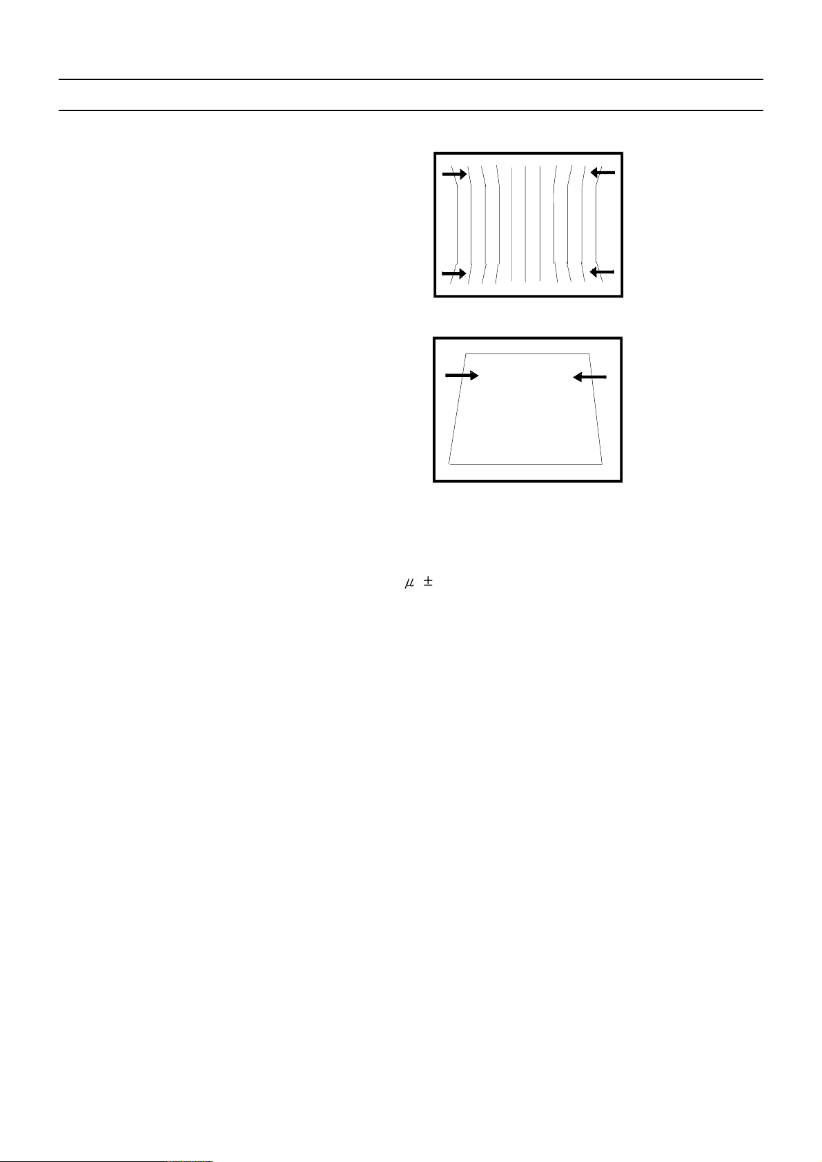
Adjust the PARABOLA, HOR WIDTH, CORNER, HOR PARAL, EW TRAPEZ, H BOW, to compensate for
geometrical distorrin,
For HOR WIDTH, adjust for 91% overscan.
Page 18
Service manual SC-150
-17-
CORNER
EW TRAPEZ
3-4-8- AGC
- Adjust the antenna signal level at 70 dB V 2
- Tune a colour bar pattern.
- Find the “AGC” item in service mode.
- Adjust AGC volume ( RB10 ) to bring the cursor to central position : 32.
Page 19
Service manual SC-150
-18-
4 - IC description
4-1 VCT383XA TV signal processor - Teletext decoder with embedded 8 bit - Controller.
4-1-1- Block diagram of the VCT
4-1-2- TV-signal Processor
Four composite video inputs, two S-VHS inputs
Analogue YC r C b input
Composite video monitor
Multistandard colour decoder ( 1 crystal )
Multistandard sync decoder
Black-line detector
Adaptive 2H comb filter Y/C separator
VIN
VRT
SGND
VSUPAF
GNDAF
VSUPD
GNDD
VERTEWPROT
HOUT
HFLB
SENSE
RSW
GNDM
VRD
XREF
Video
Front-end
Comb
Filter
Color
Decoder
Panorama
Scaler
Display
Processor
Pict. Improv
Video
Back-end
Audio
CIN
VOUT
4
22 2
3
4
2
2
3
3
RGBOUT
SVM
RGBIN
VSUPAB
GNDAB
AOUT
AIN
I
2
C
I
2
C Master
I
2
C
MSync
Color, Prio
VSync
8-bit PWM
14-bit PWM
15:1 Mux
10-bit ACD
2 Timer
2 CapCom
96 kB
CPU ROM
ADB, DB, CB
16 kB
Text
RAM
3 kB
OSD RAM
TPU
Video
24 kB ROM
31
12
1 kB
CPU RAM
CPUDMA
8
BE
RDY
Watchdog
24 IO Ports
RESQ
TEST
XTAL1
XTAL2
CLK20
CNDP1
VSUPP1
Pxy
GNDS
VSUPS
Clock
Oscillator
Reset
Logic
VCT 38xx
Page 20

Service manual SC-150
-19-
Horizontal scaling ( 0.25 to 4 )
Panoramavision
Black-level expander
Dynamic peaking
Soft limiter (gamma correction)
Colour transient impr ovement
Programmable RGB matrix
Analogue RGB/Fastblank input
Half-contrast switch
Picture frame generator
Scan velocity modulation output
High-performance H/V deflection
Angle and bow correction
Separat e ADC for tube measurements
EHT compensation
4-1-3- -Controller
8-bit, 10-Mhz CPU (65C02)
96 kB program ROM on chip
1 kB program RAM on chip
memory banking
16-input, 16-l evel interrupt controller
pat ch module for 10 ROM locations
t wo 16-bit reloadable timers
capture compare module
watchdog timer
14-bit PWM for voltage synthesis
Four 8-bit PWMs
10-bi t ADC with 15:1 input MUX
I2C bus master interface
24 programmable I/O ports
80C51
-controller core standard instruction set and timing
1 s machine cycle
32-128Kx8-bit late programmed ROM
3-12Kx8-bi t Auxiliary RAM (shared with Display and Acquisition)
Interrupt controller for ind ividual enable/disable with two level priority
Two 16-bit Timer/Counter registers
WatchDog timer
Auxiliary RAM page pointer
16-bit Data pointer
IDLE and P ower Down (PD) mode
14 bits PWM for Voltage Synthesis Tuning
8-bi t A/D converter
4 pins which can be programmed as general I/O pin, ADC input or PWM (6-bit) output
4-1-4- Teletext Features
Four programmable video inputs
Adapt ive data slicer
Signal quality detection
WST, PDC, VPS, and WSS acquisition
Page 21

Service manual SC-150
-20-
High-l evel command language
FLOF ( Fastext), and TOP support
10 pages memory on chip (10kB)
4-1-5- Display OSD Features
3kB OSD RAM on chip
WST level 1.5 compliant
WST level 2 parallel attributes
32 foreground/background colours
programmable colour look-up table
1024 mask programmable characters
17 national languages
(Latin, Cyrillic and Greek caracter sets)
Character matrix 10x10
4-color mode for user font
4-1-6- Audio Features
Three mono inputs
Two mono outputs
Programmable channel select
Volume control for one mono channel
4-1-7- General Features
Submicron CMOS technology
L ow-power standby mode
Single 20.25 MHz crystal
64-pin PSDIP package
4-1-8- Data Capture
The Video Front End section takes in the analogue Composite Video and Blanking Signal (CVBS), and from this
extracts the required data, which is then decoded and stored in memory.
The extraction of the data is performed in the digital domain. The first stage is to select and convert the analogue
CVBS signal into a digital form. This is done using 8 bit ADC sampling at 20.25 Mhz.
The digital data services transmitted in the VBI are selected and acquired separately form the video part. This is done
by the use of an adaptive data slicer. The following data types can be extracted : 625 line World System Teletext
(WST), VPS, WSS. The data is acquired and decoded by the teletext decoder (TPU), then stored in an SRAM lnterface.
4-1-9- Data Capture Features
Video Signal Quality detector
Data Capture for 625 line WST
Data Capture fo r VPS data (PDC system A)
Data C apture for Wide Screen Signalling (WSS) bit decoding
Real-time capture and decoding fo r WST Teletext in Hardware, to enable optimised microprocessor throughput
10 page memory stored On-Chip
Page 22
Service manual SC-150
-21-
IC marking
English, French,
German, Italian,
Spanish, Dutch,
Danish, Finnish,
Norwegian, Swedish,
Greek, Polish,
Hungarian, Czech,
Slovakian, Romanian,
Russian,Bulgarian
• Inventory of transmitted Teletext pages stored in the Page Table
Signal quality detector fo r WST data
Comprehensive Teletext language coverage
Full Field Vertical Blanking Interval (VBI) data capture of WST data
4-1-10- TV processor version and -Controller capacity
IC version VCT 3832A VCT 3834A
8 bit
-controller
ROM size 96k 96k
RAM size 1k 1k
PAL decoder
SECAM decoder
NTSC decoder
Picture improvement
Teletext page memory 10 pages 10 pages
Adaptive Comb filter
Panorama Scaler
4-1-11- IC marking and version
Chassis OSD languages
ATSS countries
Text
SC-150 VCT3834A
Pan-European Latin.
Cyrillic, Greek.
GB, France, Germany,
Italy, Belgium, Spain,
Austria, Poland,
Switzerland, Denmark,
Finland, Netherlands,
Norway, Sweden,
Ireland, Hungary,
Czech Republic, Others
4-1-12- Pinning
PSDIP
64-pin
1 Powe r OUT High = SMPS ON, Low = SMPS in stand by mode.
2 A GC IN For service only, tuner AGC, TOP alignment.
3 VSUPP1 SUPPLY Supply Voltage, Port ( pin 1, 2, 5, 6, 7, 8, 9, 10, 61, 62, 63, 64).
4 GNDP1 SUPPLY Ground, Port.
5 MOD_SW OUT High = Negative modulation, Lo w = Positi v e modulation (L/L’).
6 SECAM L/L’ OUT High = L’, L ow = L.
7 AFC IN
8IR IN
9 SC1.SW IN
10 SC2.SW IN
11 VOUT OUT Analog Video Output
12 VRT IN Reference Voltage Top, Video ADC
13 SGND IN Signal Ground for Analog Input
Pin Name
Type
Short Description
X
Page 23
Service manual SC-150
-22-
14 GNDAF SUPPLY Ground, Analog Front-end
15 VSUPAF SUPPLY Supply V oltage, Analog Front-end
16 CBIN IN Analog Component Cb Input
17 CIN1 IN Analog Chroma 1 Input
18 CIN2/CRIN IN Analog Chroma 2 Input / Analog Component Cr Input
19 VIN1 IN Analog Video 1 Input
20 VIN2 IN Analog Video 2 Input
21 VIN3 IN Analog Video 3 Input
22 VIN4 IN Analog Video 4 Input
23 TEST IN Test Pin, Reserved For Test
24 HOUT OUT Horizontal Drive Output
25 VSUPD SUPPLY Supply V oltage, Digital Circuitry
26 GNDD SUPPLY Ground, Digital Circuitry
27 FBLI N IN Fast Blank Input
28 RIN IN Analog Red Input
29 GIN I N Analog Green Input
30 BIN IN Analog Blue Input
31 VP R OT IN V ertical Protection Input
32 SAFETY IN Safety Input
33 HFLB IN Horizontal Flyback Input
34 VERTQ/ INTLC OUT Dif ferential Vertical Sawtooth Output Interlace Control Output
35 VE RT OU T Differential Vertical Sawtooth Output
36 EW OUT Vertical Parabola Output
37 SENSE IN Sense ADC Input
38 GNDM SUPPLY Ground, MADC Input
39 RSW1 OUT Range Switch1 for Measurement ADC
40 RSW2 OUT Range Switch2 for Measurement ADC
41 SVMOUT OUT Scan V elocity Modulation Output
42 R O UT OUT Analog Red Output
43 GOUT OUT Analog Green Output
44 BOUT OUT Analog Blue Output
45 VSUPAB SUPPLY Supply V oltage, Analog Back-end
46 GNDAB SUPPLY Ground, Analog Back-end
47 VRD IN DA C Reference
48 XREF IN Reference Input for RGB DACs
49 AIN3 IN Analog Audio 3 Input
50 AIN2 IN Analog Audio 2 Input
51 AIN1 IN Analog Audio 1 Input
52 AOUT2 OUT Analog Audio 2 Output
53 AOUT1 OUT Analog Audio 1 Output
54 VSUPS SUPPLY Supply V oltage, Standby
55 GNDS SUPPLY Ground, Standby
56 XTAL1 IN Analog Crystal Input
57 XTAL2 OU T Analog Crystal Output
58 RESQ IN/OUT Reset Input/Output, Activ e Low
59 SCL IN/OUT I 2 C Bus Clock
60 SDA IN/OUT I 2 C Bus Data
61 Mute OUT High = Mute activ e
62 LED OUT High = Green, Lo w = Red
63 KB IN Local keyboard ADC input
64 OC P IN Over Current Protection input
Pin Name
Type
Short Description
PSDIP
64-pin
Page 24
Service manual SC-150
-23-
OCP64
63
62
61
60
58
57
56
55
48
46
45
44
43
42
41
40
39
38
37
36
34
35
33
47
54
53
52
51
50
49
59
KB
LED
MUTE
SDA
SCL
RESET
XTAL in
OSC GND
GND
S/B 3.3V
GND
GND
GND
XREF
VRD
GND
5V
B out
G out
R out
SVM out
RSW2
RSW1
GND
SENSE
EW
VERTQ
VERT
HFLB
Power1
2
3
4
5
7
8
9
10
17
19
20
21
22
23
24
25
26
27
28
29
31
30
32
18
11
12
13
14
15
16
6
AGC
S/B 5V
Gnd
MOD SW
SECAM L
AFC/RES
IR
SC1 SW
SC2 SW
Vout
VRT
SGND
GND
5V
Cb in
C in
Cr in
IF-IN
SC1-IN
SC2-IN
RCA VIN
TEST
H out
3.3 V
GND
FBLIN
Rin
Gin
Bin
VPROT
SAFETY
VCT 383X
Page 25

Service manual SC-150
-24-
4-2 MSP341x Multistandard Sound Processor
The MSP 341x is designed as a single-chip Multistandard Sound Processor for applications in analogue and digital TV
sets, video recorders, and PC cards.
The MSP3411 has all functions of MSP3410 with the addition of a virtual surround sound feature.
A Surround sound affect can be rc produced with two loudspeakers. The MSP3411 includes virtualizer
algorithm “3D Panorama” which has been approved by the Dolby laboratories for compliance with the “Virtual Dolby
Surround” technolo gy. In addition, the MSP3411 includes Micronas “Panorama” algorithm.
MSP 341x features :
- sound IF input
- No external filters required
- Stereo baseband input via integrated AD converters
- Two pairs of DA converters
- Two carrier FM or NICAM processing
- AVC : Automatic Volume Correction
- Bass, treble, volume processing
- Full SCART in/out matrix without restrictions
- Improved FM-identification
- Demodulator short programming
- Autodetection for terrestrial TV - sound standards
- Precise bit-error rate indication
- Automatic switching from NICAM to FM/AM or vice versa
- Improved NICAM synchronisation algorithm
- Improved carrier mute algorithm
- Improved AM-demodulation
- Reduction of necessary controlling
- Less external components
4-2-1- Basic Features of the MSP 341x
4-2-1-1 Demodulator and NICAM Decoder Section
The MSP 341x is designed to simultaneously perform digital demodulation and decoding of NICAM-coded TV stereo
sound, as well as demodulation of FM or AM mono TV sound. Alternatively, two carrier FM systems according to the
German terrestrial specs can be processed with the MSP 341x.
The MSP 341x facilitates profitable multistandard capability, offering the following advantages:
- Automatic Gain Control (AGC) for analogue input: input range: 0.10 - 3 Vpp
- integrated A/D converter for sound-IF input
- all demodulation and filtering is performed on chip and is individually programmable
- easy realisation of all digital NICAM standards (B/G, I, L and D/K)
- FM-demodulation of all terrestrial standards (include identification decoding)
- no external filter hardware is required
- only one crystal clock (18.432 MHz) is necessary
Page 26

Service manual SC-150
-25-
- high deviation FM-mono mode (max. deviation: approx. ±360 kHz)
4-2-1-2 DSP-Section (Audio Baseband Processing)
- flexible selection of audio sources to be processed
- performance of terrestrial de-emphasise systems (FM, NICAM)
- digitally performed FM-identification decoding and de-matrixing
- digital baseband processing: volume, bass, treble
- simple controlling of volume, bass, treble
4-2-1-3 Analogue Section
- two selectable analogue pairs of audio baseband input (= two SCART inputs) input level: <2 V RMS,
input impedance: >25
- one selectable analogue mono input (i.e. AM sound): Not used in this chassis
- two high-quality A/D converters, S/N-Ratio: >85 dB
- 20 Hz to 20 kHz bandwidth for SCART-to-SCART copy facilities
- loudspeaker: one pair of four-fold oversampled D/A converters. Output level per channel:
max. 1.4 VRMS output resistance: max. 5
. S/N-ratio: >85 dB at maximum volume Max.
noise voltage in mute mode: < 10 V (BW: 20 Hz... 16kHz)
- one pair of four-fold oversampled D/A converters supplying a pair of SCART-outputs.
output level per channel: max. 2 V RMS, output resistance: max. 0.5 , S/N-Ratio: >85 dB (20 Hz... 16 kHz)
4-2-1-4 NICAM plus FM/AM-Mono
According to the British, Scandinavian, Spanish, and French TV-standards, high-quality stereo sound is transmitted
digitally. The systems allow two high-quality digital sound channels to be added to the already existing
FM/AM-channel. The sound coding follows the format of the so-called Near Instantaneous Companding System
(NICAM 728). Transmission is performed using Differential Quadrature Phase Shift Keying (DQPSK. Table below
offers an overview of the modulation parameters.)
In the case of NICAM/FM (AM) mode, there are three different audio channels available: NICAM A, NICAM B, and
FM/AM-mono. NICAM A and B may belong either to a stereo or to a dual language transmission. Information about
operation mode and about the quality of the NICAM signal can be read by the controlling software via the control bus.
In the case of low quality (high bit error rate), the controlling software may decide to switch to the analogue FM/AMmono sound. Alternatively, an automatic NICAM-FM/AM switching may be applied.
4-2-1-5 German 2-Carrier System (DUAL FM System)
Since September 1981, stereo and dual sound programs have been transmitted in Germany using the 2-carrier system.
Sound transmission consists of the already existing first sound carrier and a second sound carrier additionally
containing an identification signal. More details of this standard are given in Tables below. For D/K very similar
system is used.
Page 27
Service manual SC-150
-26-
TV standards
TV Position of sound Sound modulation Color system Country
system carrier (MHz)
B/G 5.5 / 5.7421875 FM Stereo PAL Germa ny
B/G 5.5 / 5.85 FM-Mono / NICAM PAL Scandinavia,
Spain
L 6.5 / 5.85 AM-Mono / NICAM SECAM-L France
I 6.0 / 6.552 FM-Mono / NICAM PAL UK
D/K 6.5 / 6.2578125 D/K1 FM Stereo SECAM-East USSR
6.5 / 6.7421875 D/K2
6.5 / 5.85 D/K-NICAM FM-Mono / NICAM Hungary
Pin connections and short description
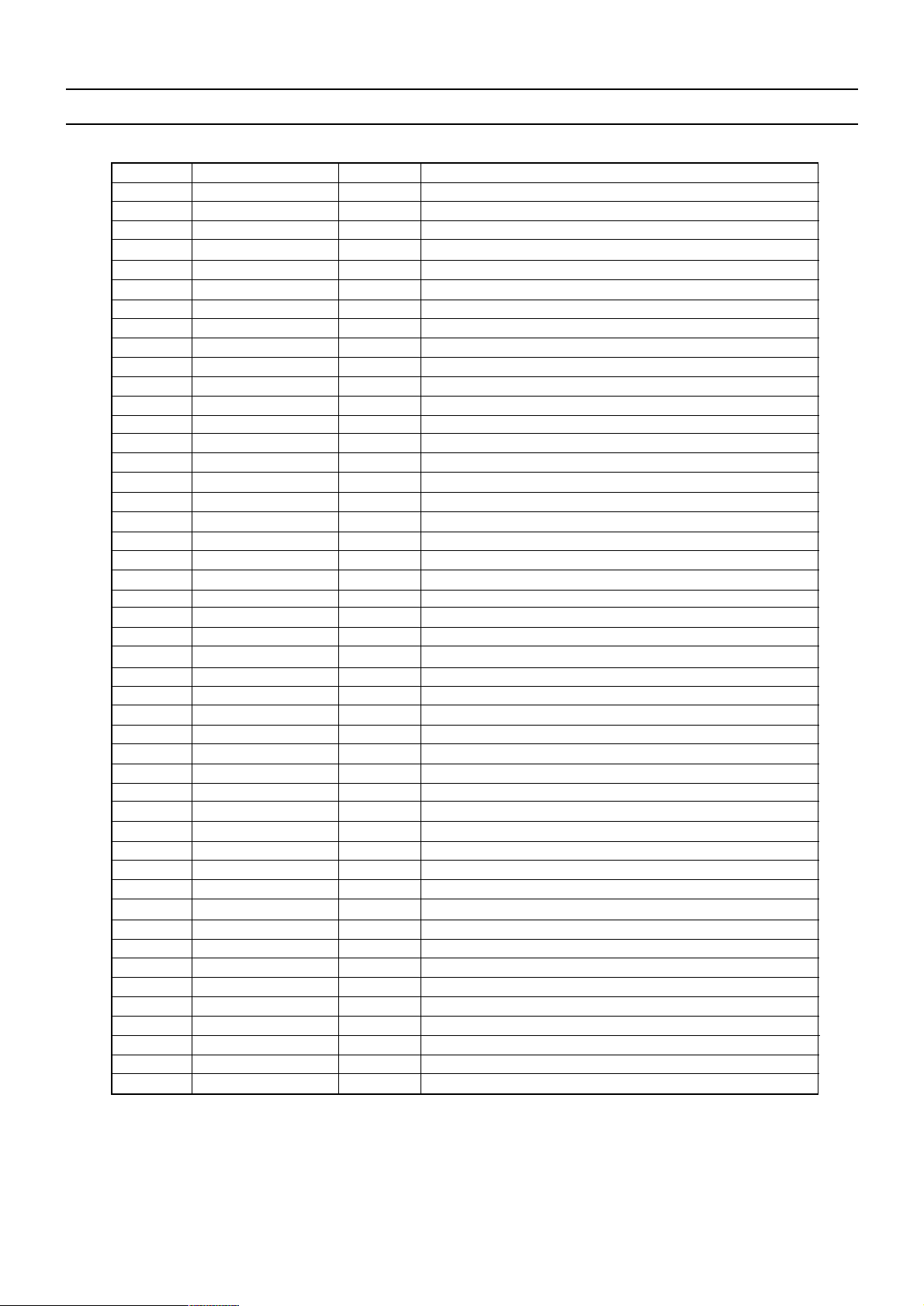
Pin No. Pin Name Type Short description
1 T P Out Test pin
2 N C Not Connected
3 N C Not Connected
4 T P Out Test pin
5 T P Out Test pin
6 ADR_SEL In I2C bus Address select
7 STANDBYQ In Standby ( Low-active)
8 N C Not Connected
9 I2C_CL In / Out I2C Clock
10 I2C_DA In / Out I2C data
11 T P In / Out Test pin
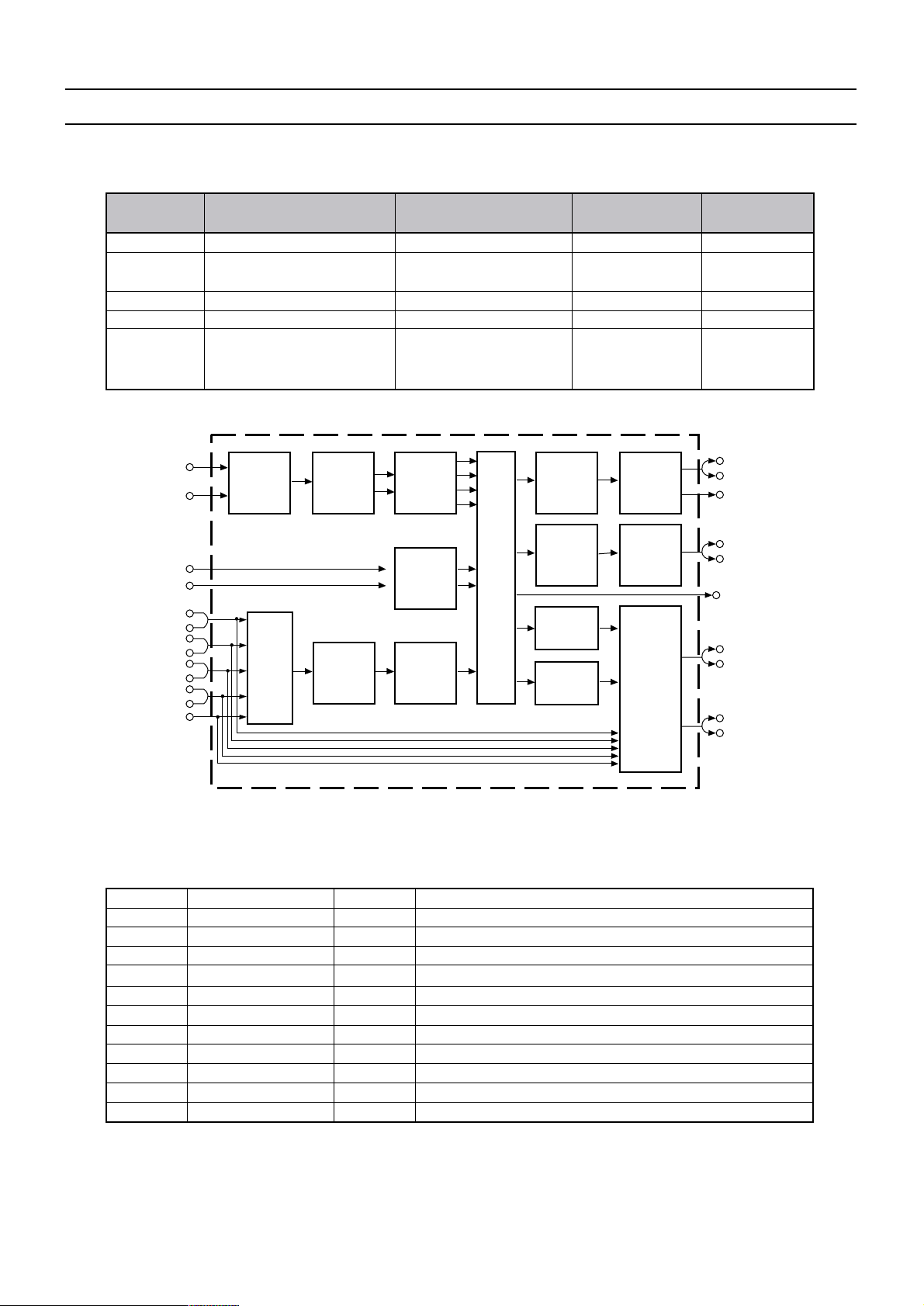
Sound IF 1
ADC
ADC
DAC
DAC
Loud-
speaker
sound
Processing
Headphone
sound
Processing
DAC
SCART
Output
Select
DAC
DSP
SCART
input
Select
De-
modulator
Pre-
processing
Prescale
Prescale
Sound IF 2
I
2
S2
SCART1
SCART2
SCART3
SCART4
MONO
I2S1
I
2
S
Loudspeaker
Subwoofer
Headphone
SCART1
SCART2
Source Select
Architecture of MSP341x
Page 28
Service manual SC-150
-27-
12 TP In / Out Test pin
13 TP Out Test pin
14 NC Not Connected
15 TP Out Test pin
16 TP Out Test pin
17 TP Out Test pin
18 DVSUP Digital power supply +5V
19 DVSS Digital Ground
20 NC Not Connected
21 NC Not Connected
22 NC Not Connected
23 NC Not Connected
24 RESETQ In Power-On-reset
25 NC Not Connected
26 NC Not Connected
27 VREF2 Reference ground 2 high voltage part
28 DACM_R Out Loudspeaker out Right
29 DACM_L Out Loudspeaker out Left
30 NC Not Connected
31 TP Out Test pin
32 NC Not Connected
33 NC Not Connected
34 NC Not Connected
35 VREF1 Reference ground 1 high voltage part
36 SC1_OUT_R Out Scart output 1, right
37 SC1_OUT_L Out Scart output 1, left
38 NC Not Connected
39 AHVSUP Analog power supply 8.0V
40 CAPL_M Volume capacitor MAIN
41 AHVSS Analog ground
42 AGNDC Analog reference voltage high voltage part
43 NC Not Connected
44 NC Not Connected
45 NC Not Connected
46 NC Not Connected
47 NC Not Connected
48 ASG2 Analog Shield Ground 2
49 SC2_IN_L In Scart input 2 in, left
50 SC2_IN_R In Scart input 2 in, right
51 ASG1 Analog Shield Ground 1
52 SC1_IN_L In Scart input 1 in, left
53 SC1_IN_R In Scart input 1 in, right
54 VREFTOP Reference voltage IF A/D converter
55 MONO_IN In Mono input
56 AVSS Analog ground
57 AVSUP Analog power supply
58 ANA_IN1+ In IF input 1
Pin No. Pin Name Type Short description
Page 29
Service manual SC-150
-28-
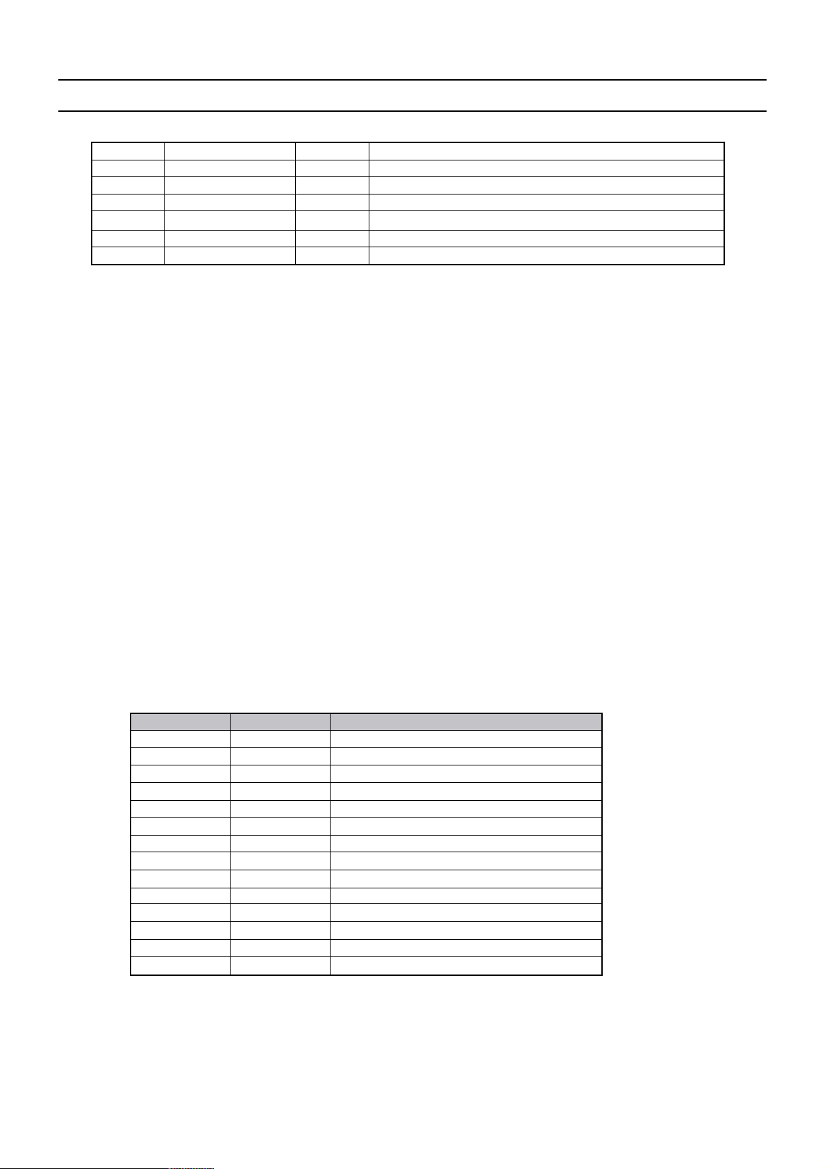
Pin No. Pin Name Type Short description
59 ANA_IN1- I n IF common
60 N C Not Connected
61 TESTEN In Test pin
62 XTAL_IN In Crystal oscillator
63 XTAL_OUT Out Crystal oscillator
64 N C Test pin
4-3 TDA 4470-Multistandard Video-IF and Quasi Parallel Sound Processor
4-3-1- Description
The TDA 4470 is an integrated bipolar circuit for multi-standard video/sound IF (VIF/SIF) signal processing in
TV/VCR and multimedia applications. The circuit processes all TV video IF signals with negative modulation
(e.g., B/G standard), positive modulation (e.g., L standard) and the AM, FM/NICAM sound IF signals.
4-3-2- Features
- 5V supply voltage ; low power consumption.
- Active carrier generation by FPLL principle (frequency-phase-locked-loop) for true synchronous demodulation.
- Very linear video demodulation, good pulse response and excellent intermodulation figures.
- Alignment-free AFC without external reference circuit, polarity of the AFC curve is switchable.
- VIF-AGC for negative modulated signals (peak sync. detection) and for positive modulation
(peak white/black level detector).
- Tuner AGC with adjustable take over point.
- Alignment-free quasi parallel sound (QPS) mixer for FM/NICAM sound IF signals.
- Intercarrier output signal is gain controlled (necessary for digital sound processing).
- Complete alignment-free AM demodulator with gain controlled AF output.
- Separate SIF-AGC with average detection
- Two independent SIF inputs
- Parallel operation of the AM demodulator and QPS mixer (for NICAM-L stereo sound).
4-3-3- Pinning
Pin Symbol Function
1,2 V
i,SIF1
SIF1 input ( symmetrical)
3V
SW
Input selector switch
4,9,16 GND Ground
5V
AGC
SIF-AGC (time constant)
6,7 V
i,VIF
VIF input (symmetrical)
8C
AGC
VIF-AGC (time constant)
10 R
TOP
Take Over Point, tuner AGC
11 I
tun
Tuner AGC output current
12 V
O,VID
Video output
13 V
SW
Standard switch
14 V
SW
L’switch
15 C
bl
Black level capacitor
17 C
ref
Internal reference voltage
18 LF Loop Filter
Page 30
Service manual SC-150
-29-
Pin Symbol Function
19 V
SW
AFC switch
20, 21 V
VCO
VCO circuit
22 V
AFC
AFC output
23 V
S
Supply voltage
24 V
O, FM
Intercarrier output
25 V
O,AM
AF output-AM sound
26 R
COMP
Offset compensation
27, 28 V
i,SIF2
SIF2 input (symmetrical)
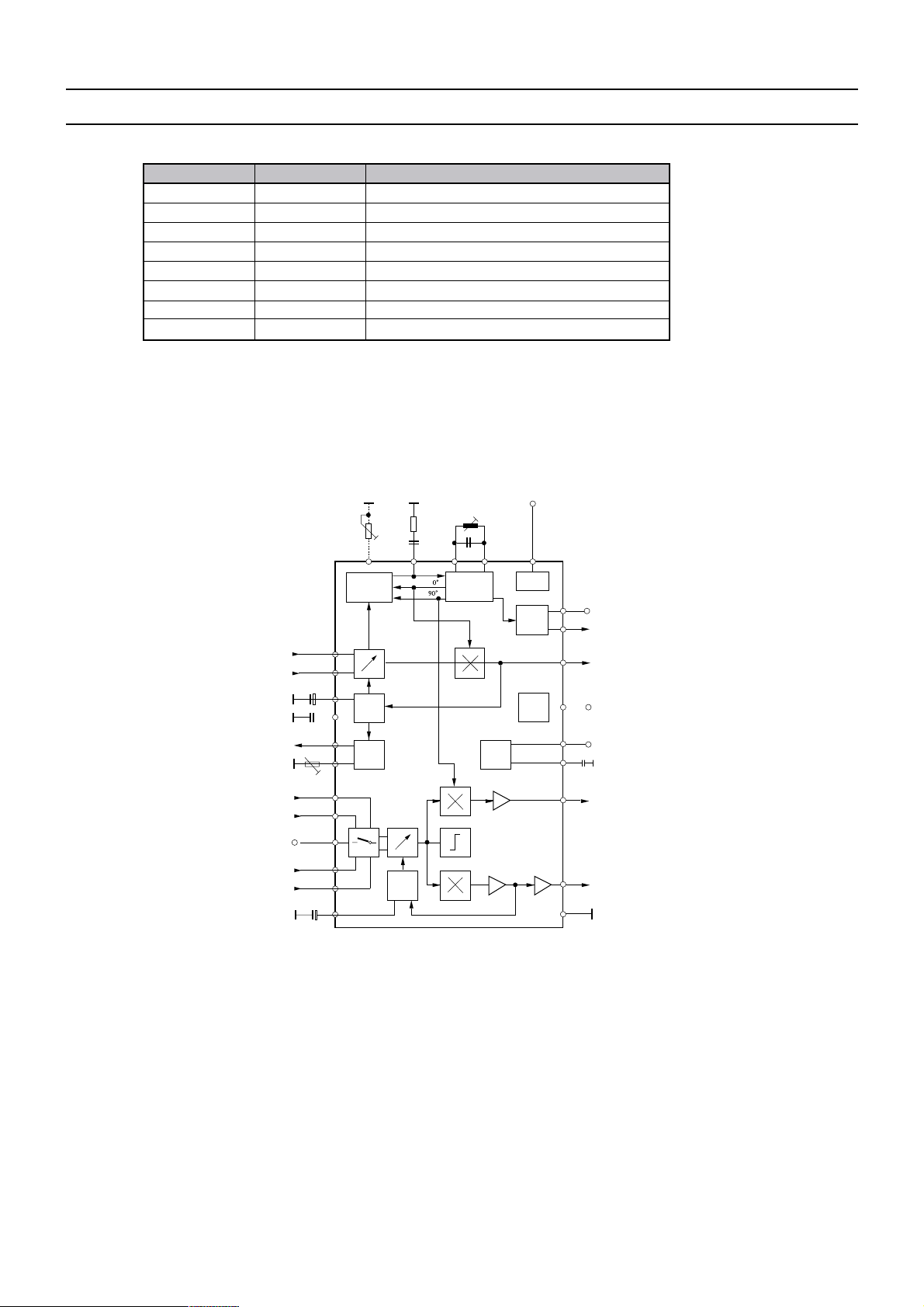
4-3-4 Block diagram
Offset
26 18 20
21 14
VCO
l' switch
VCO
Control
phase shift
FPLL
VIF amp
Loop
filter
comp.
(optional)
+
4,9,16AM det.
FM det.
25
24
17
C
ref
23
13
22
19
6
7
8
15
11
10
27
28
3
1
2
SIF 1
C
AGC
5
Standard
Video det.
VIF
C
AGC
C
BL
AGC
(VIF)
Tuner
AGC
AGC
(SIF)
Tuner
SIF 2
SIF input
switch
SIF amp
Take over
point
Video
AFC
AFC
switch
AFC
Supply
Standard
switch
V
AF
(AM)
Intercarrier
(FM/NICAM)
Page 31
Service manual SC-150
-30-
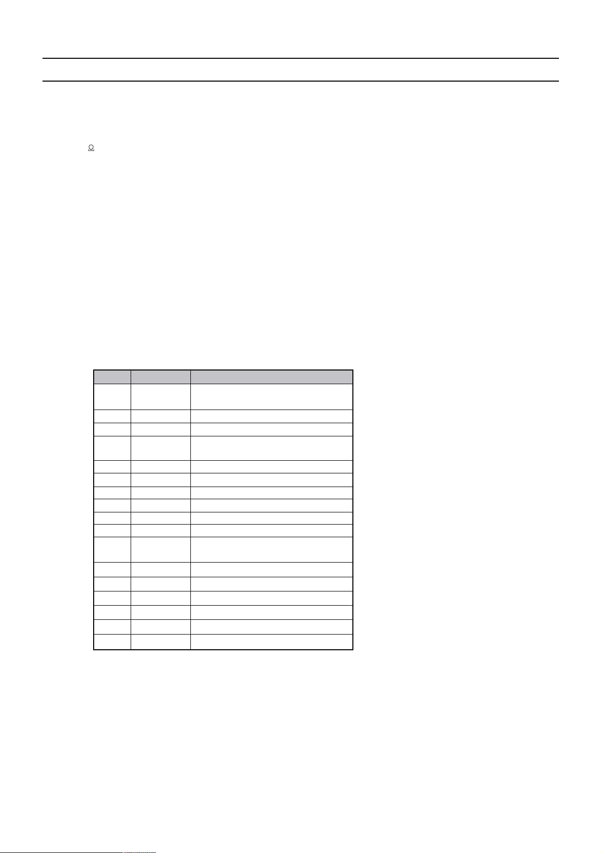
Pin Symbol Description
1 OUT1-
negative loudspeaker
terminal 1
2 GND1 ground channel 1
3 Vcc1 supply v olta ge channel 1
4
OUT1+
positive loudspeaker
terminal 1
5 n.c. not connected
not connected
6 IN1+ poitive input1
7
n.c. not connected
8 IN1- negative input1
9 IN2- negative input2
10 MO DE mode selection input
11 SVR
half supply voltage
decoupling (ripple rejection)
1
13
14
15
16
17
2
IN2+
n.c
OUT2-
nogative loudspeaker terminal 2
ground channel 2
supply voltage channel 2
positive loudspeaker terminal 2
GND2
Vcc2
OUT2+
positive input2
4-4 TDA8946JStereo Audio Amplifier
The TDA8946J is a dual-channel audio po wer amplifier with an output power of 2 X 15W
at an 8 load and a 18V supply. The circuit contains two Bridges Tied Load(BTL) amplifiers with an all-NPN output
stage and standby/mute logic. The TDA8946J comes in a 17-pin DIL power package.
4-4-1- Features
- F ew external components
- F ixed gain
- Standby and mute mode
- No on/off switching pop noise
- low standby current
- High supply voltage ripple rejection
- Outputs short-circuit protected to ground, supply and across the load
- Thermally protected
Pin description
Page 32
Service manual SC-150
-31-
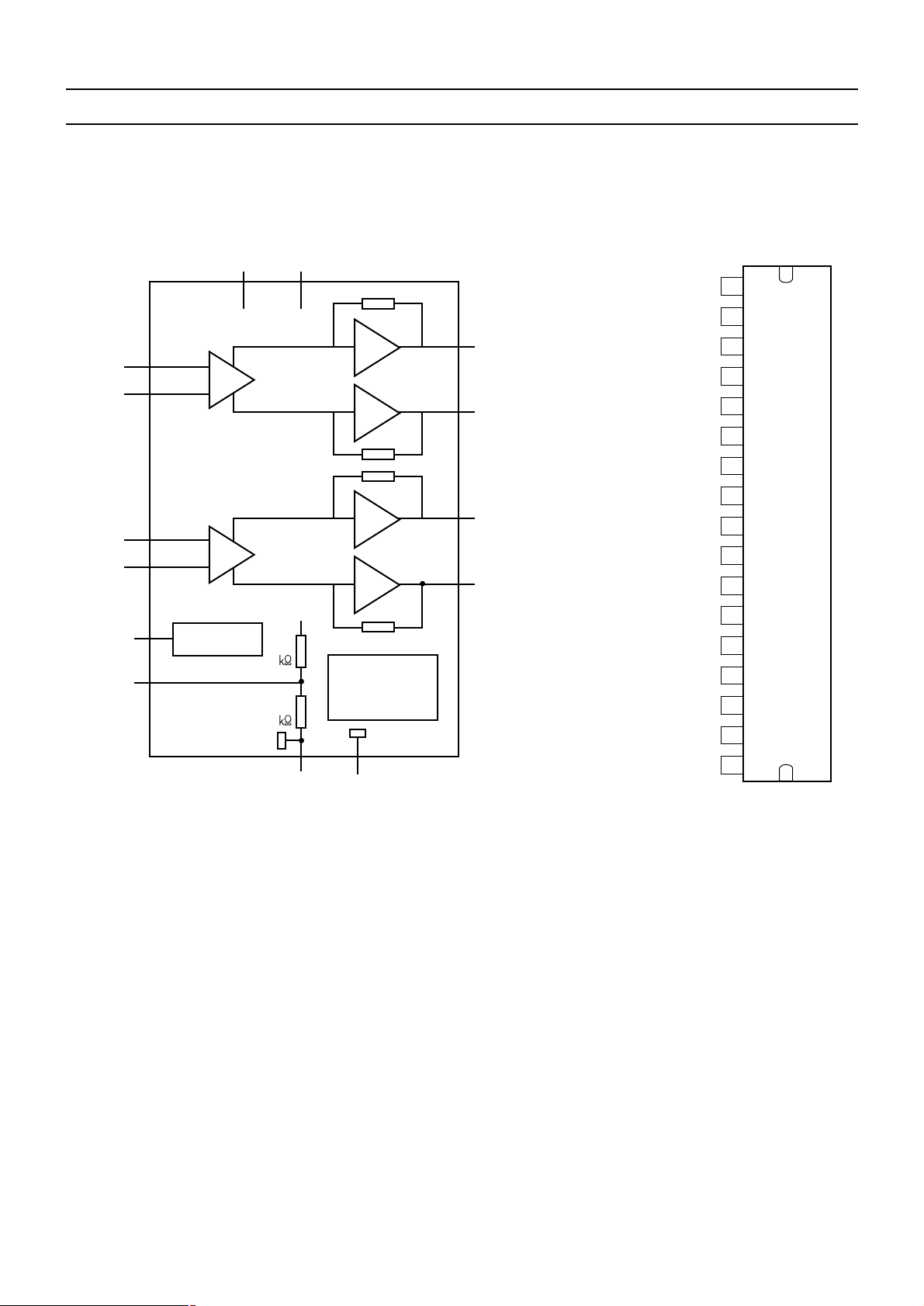
Block diagram TDA8946J Pin configuration
316
Vcc1 Vcc2
IN1-
OUT1-
OUT1-
OUT1+
OUT2-
OUT2+
IN1+
IN1IN2-
MODE
SVR
IN2+
n.c.
n.c.
n.c.
GND
GND2
GND1 GND2
Vcc1
Vcc2
OUT1+
OUT2-
OUT2+
IN1+
IN2IN2+
MODE
SVR
11
10
STANDBY/
MUTE LOGIC
20
Vcc
15
SHORT CIRCUIT
AND
TEMPERATURE
PROTECTION
20
17
14
4
1
8
6
9
12
TDA8946J
TDA8946J
MBK933
1
2
3
4
5
6
7
8
9
10
11
12
13
14
15
16
17
4-5 TDA8358J Vertical Amplifier
The TDA8358J are power circuit for use in 90
o
and 110o colour deflection systems for field frequencies
of 25 to 200Hz and 16/9 picture tubes. The circuit provides a DC driven vertical deflection output circuit,
operating as a highly efficient class G system. Due to the full bridge output circuit the deflection coils can
be DC coupled.
The IC is constructed in a Low Voltage DMOS process that combines Bipolar, CMOS and DMOS devices.
MOS transistors are used in the output stage because of the absence of second breakdown.
Page 33

Service manual SC-150
-32-
4-5-1 TDA8358J
An East-West output stage is provided that is able to sink current
from the diode modulator circuit.
Features :
- Few external components
- Highly efficient fully DC-coupled vertical output bridge circuit
- Short rise and fall time of the vertical flyback switch
- Guard circuit
- Temperature (thermal) protection
- High EMC because of common mode inputs
- East-West output stage
Page 34
Service manual SC-150
-33-
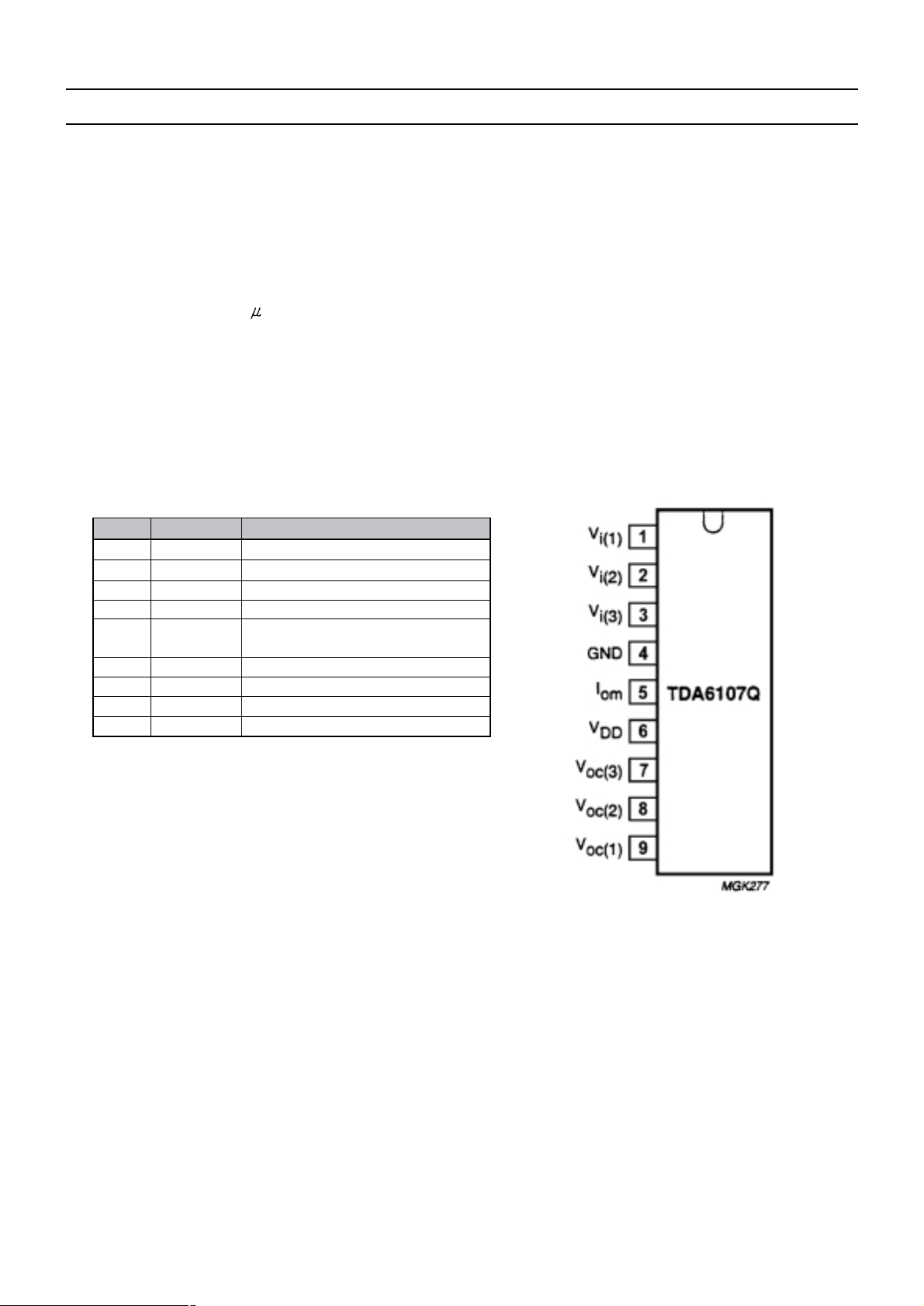
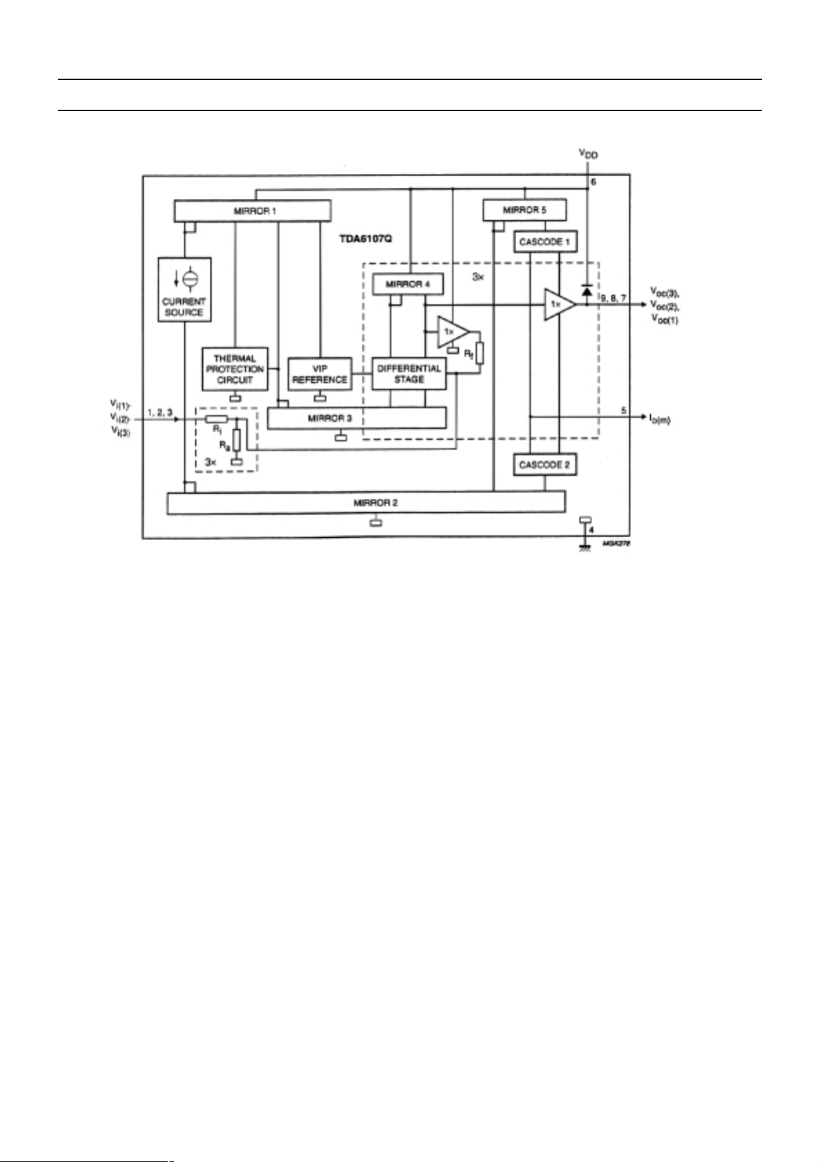
4-6 TDA6107Q
The TDA6107Q includes three video output amplifiers in one plastic DIL-Bent-SIL 9-pin medium power package,
using high voltage DMOS technology, and is intended to drive the three cathodes of a colour CRT directly. To obtain
maximum performance, the amplifier should be used with black-current control.
Features
- Typical bandwidth of 5.5 MHz for an output signal of 60 Vpp
- High slew rate of 900V/ s
- No external components required
- Very simple application
- Single supply voltage of 200V
- Internal reference voltage of 2.5 V
- Fixed gain of 50.
- Black-current stabilisation (BCS) circuit
- Thermal protection
Pin description
Pin Symbol Description
1V
i(1)
inverting input 1
2V
i(2)
inverting input 2
3V
i(3)
inverting input 3
4 GND ground (fin)
5I
om
black current
measurement output
6V
DD
supply voltage
7V
OC(3)
cathode output 3
8V
OC(2)
cathode output 2
9V
OC(1)
cathode output 1
Page 35
Service manual SC-150
-34-
Block diagram TDA6107Q
Page 36
Service manual SC-150
-35-
4-7 24C16 - 16 Kb EEPROM
features :
- 16 Kbit serial I2C bus EEPROM
- Single supply voltage : 4.5 V to 5.5 V
- 1 Million Erase/Write cycles (minimum)
- 40 year data retention (minimum)
Pin description
Pin No. Name Description
1, 2, 3 E0, E1, E2 Device address - not used
5 SDA Serral Data/Address Input/Output
6 SC L Serial clock
7 WC Write control
8 Vcc Supply voltage
4 Vss Ground
The memory device is compatible with the I2C memory standard. This is a two wire serial interface that uses a
bi-directionnal data bus and serial clock. The memory carries a built-in 4-bit unique device type identifier code (1010)
in accordance with the I2C bus definition.
Serial Clock (SCL)
The SCL input is used to strobe all data in and out of the memory.
Serial Data (SDA)
The SDA pin is bi-directionnal, and is used to transfer data in or out of the memory
Page 37
Service manual SC-150
-36-
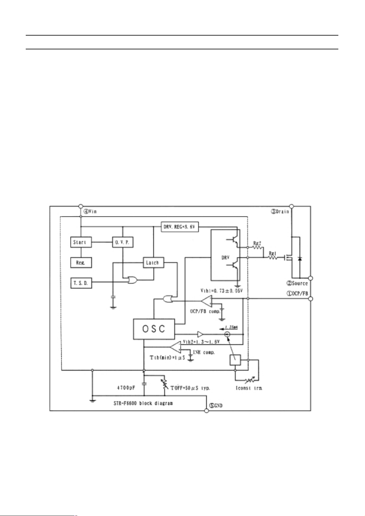
4-8 STR - F6653
4-8-1 General description
The STR-F6653 is an hybrid IC with a build-in MOSFET and control IC, designed for flyback converter type switch
mode power supply applications.
4-8-2 Features
- Small SIP fully isolated molded 5 pins package
- Many protection functions :
* Pulse-by-pulse overcurrent protection (OCP)
* Overvoltage protection with latch mode (OVP)
* Thermal protection with latch mode (TSD)
4-8-3 Block diagram
Page 38
Service manual SC-150
-37-
4-8-4 Pins description
pin name symbol description
1 Overcurrent / feedback O.C.P./ F.B. Input of over current detection signal and
feedback signal
2 Source S MOSFET source
3 Drain D MOSFET drain
4 Supply V
IN
Input of power supply for control circuit
5 Ground GN D Ground
4-8-5 Control part electrical characteristics
IC PIN RATING
NUMBER MIN. TYPE MAX
Operation start voltage 4-5 V
IN
(on) 14.4 1 6 17.6 V
Operation stop voltage 4-5 V
IN
(off) 9 1 0 111 V
Circuit current in 4-5 I
IN
(on) - - 30 m A
operation
Circuit current in non- 4-5 I
IN
(off) - - 100 mA A
operation
Maximum OFF time - T
OFF
(max) 45 - 55 SEC
Minimum time for input of 1-5 T
TH
(2) - - 1.0 SEC
quaxi resonant signals
Minimum off time - T
OFF
(min) - - 1.5 SEC
O.C.P./F.B. terminal 1-5 V
TH
(1) 0.68 0.73 0.78 V
threshold voltage 1
O.C.P./F.B. terminal 1-5 V
TH
(2) 1.3 1.45 1.6 V
threshold voltage 2
O.C.P./F.B. terminal extraction 1-2 I
OCP/FB
1.2 1.35 1.5 mA
current
O.V.P. operation voltage 4-5 V
IN
(OVP) 20.5 22.5 24.5 V
Latch circuit sustaining voltage 4-5 I
IN
(H) - - 40 0 A
Latch circuit release voltage 4-5 V
IN
(La.off) 6.6 - 8.4 V
Thermal shutdown operating - T
J
(TSD) 140 - -
0
C
temperature
SYMBOL
UNIT
DESCRIPTION
Page 39
Service manual SC-150
-38-
DESCRIPTION
4-8-6 MOSFET electrical characteristics
IC PINS RATING
NUMBER MIN. TYPE MAX
Drain-to-source break 3-2 V
DSS
650 - - V
voltage
Drain leakage current 3-2 I
DSS
- - 300 A
On-resistance 3-2 R
DS
(on) - - 1.95
Switching time 3-2 tf - - 2 50 noec
Thermal resistance - O
CH
-F - - 0.95
0
C/W
SYMBOL
UNIT
Page 40
Service manual SC-150
-39-
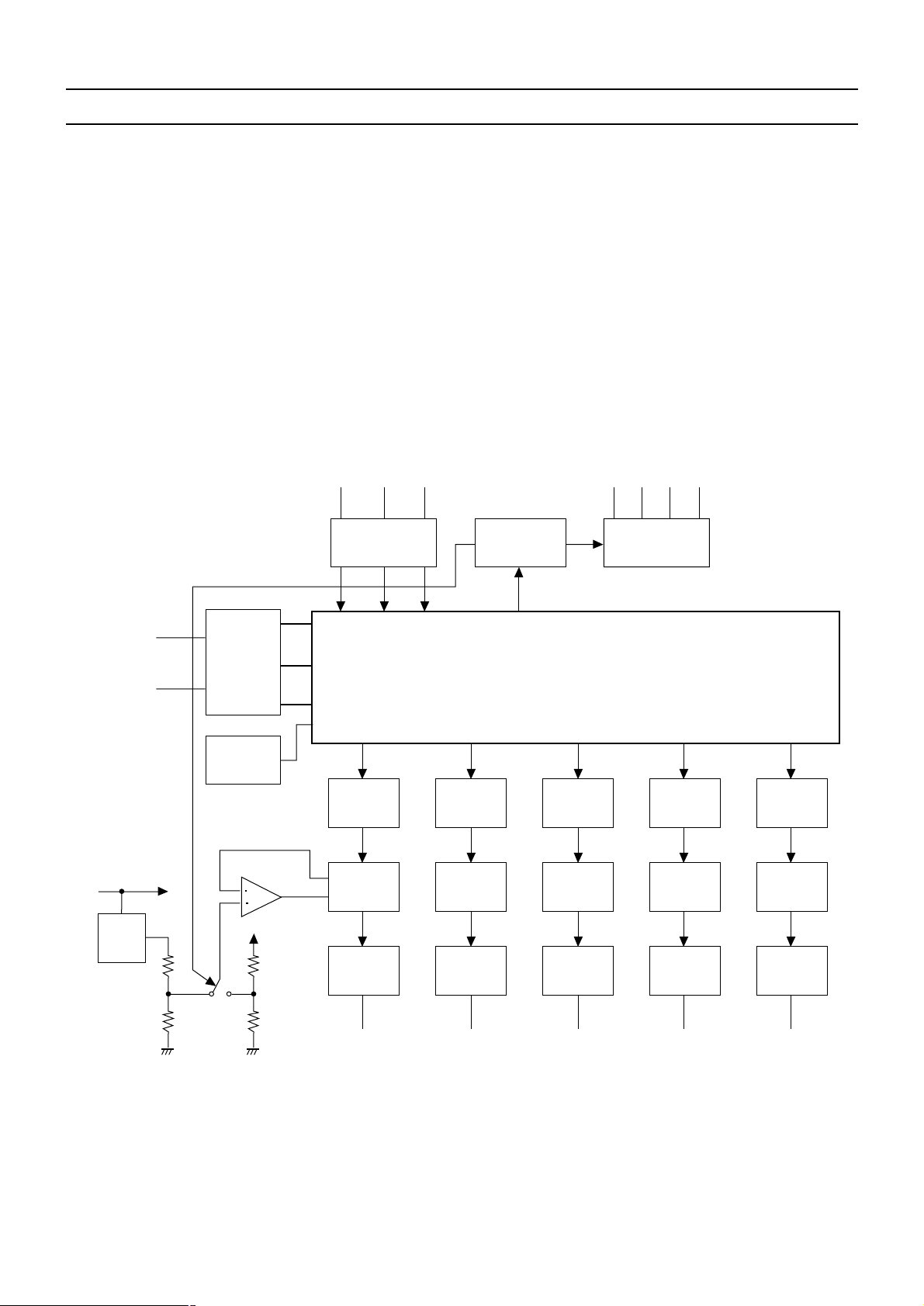
4-9 CXA1315P
4-9-1 General description
The CXA1315M/P is developed as a 5-channel 8- bit D/A converter supporting with I 2 C bus.
4-9-2 Features
-Serial control through I
2 C bus
-5-channel 8-bit D/A converter
-Built-in 4general-purpose I/O ports (Digital I/O)
-I/O can be specified to respective ports independently
-Selection of 8 slave addresses possible through address select pins (3 pins)
4-9-3 Block diagram
Level
Conversion
Level
Conversion
Power On
Reset
SAD2
SDA
I
2
C BUS
SCL
LATCH
DAC
REG
DAC4
GND
DAC3 DAC2 DAC1 DAC0
AMP
Vcc
Vcc
AMP AMP AMP AMP
DAC DAC DAC DAC
LATCH LATCH LATCH LATCH
SAD1 SAD0 SW0 to 3
Open collector
Level
Conversion
LATCH
I2C Decoder
Page 41
Service manual SC-150
-40-
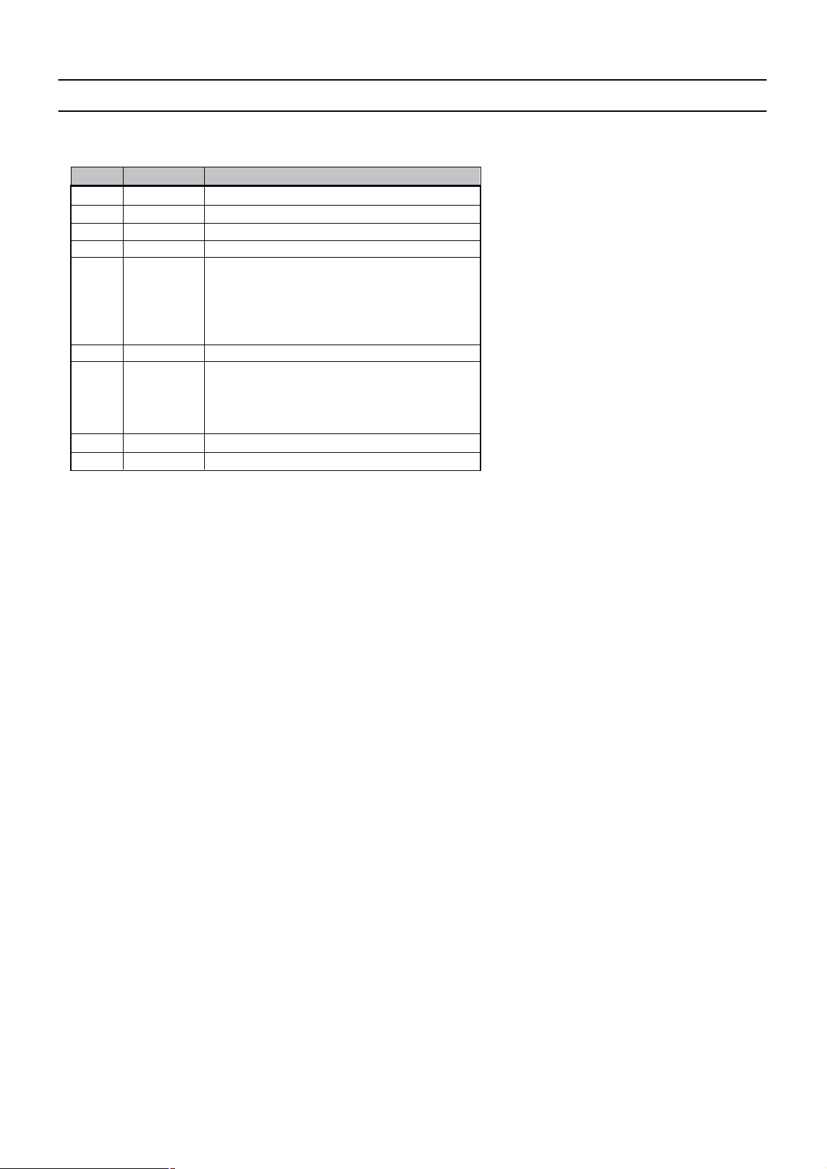
4-9-4 Pin Description
Pin Symbol Description
I/O pin for general purpose I/O port
1 SW1
2 SW0
VILmax: 1.5V
9 SW2
VIHmin: 3V
10 SW3
VOLmax: 0.4V
10 GND
11 SDA0
GND pin
12 SDA1
13 SDA2
15 SCL
Slave address input pin
Input at positive logic
VILmax: 1.5V
VIHmin: 3V
SCL input pin for I2C bus
Power supply pin
16 Vcc
3 DAC4
4 DSC3
5 DAC2
6 DAC1
7 DAC0
D/A converter output pin
Page 42
Service manual SC-150
-41-
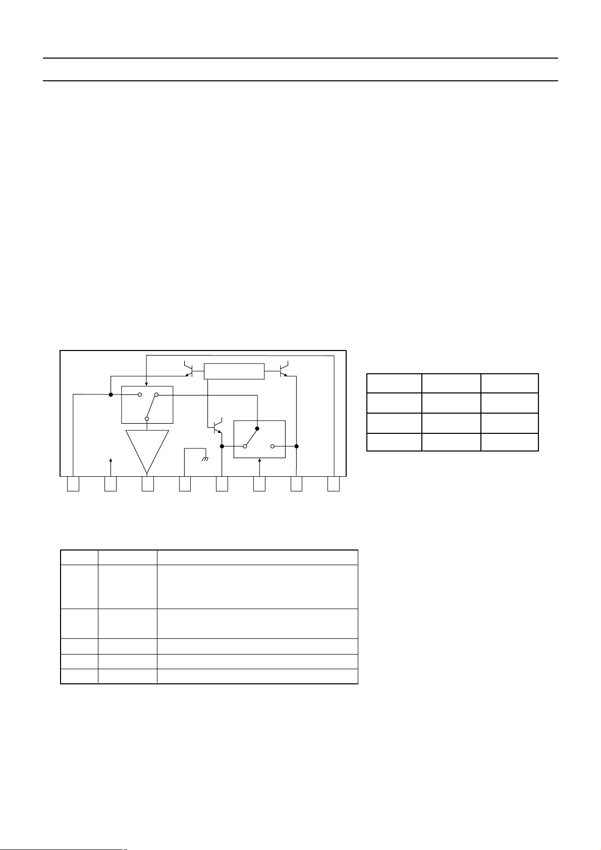
4-10 MM1118
4-10-1 General description
This is a 3-input, 1-output video switch IC with a clamp function and built-in 6dB amp, for video signal switching.
One of the inputs also has a mute function.
4-10-2 Features
-Built-in 6dB amp
-Clamp function
-Mute function
-Current consumption: 5.1mA typ.
-Operating power supply voltage range: 4.6~13.0V
-Frequency response: 10MHz
-Crosstalk: 64dB (at 4.43MHz)
4-10-3 Block diagram
4-10-4 Pin Description
12345678
IN3 Vcc OUT GND IN1 SW1 IN2 SW2
SW1
Control input trurh table
L
H
L
L
H
IN1
IN2
IN3
"
SW2 OUT
Clamp
Clamp
Clamp
SW
SW
Buffer
Bias
Pin Symbol Description
Input1
5 IN1
7 IN2
Input2
1 IN3
Input3
6 SW1
Switch1
8 SW2
Switch2
2 Vcc Power supply
3 OUT Output
Ground
4 GND
Page 43
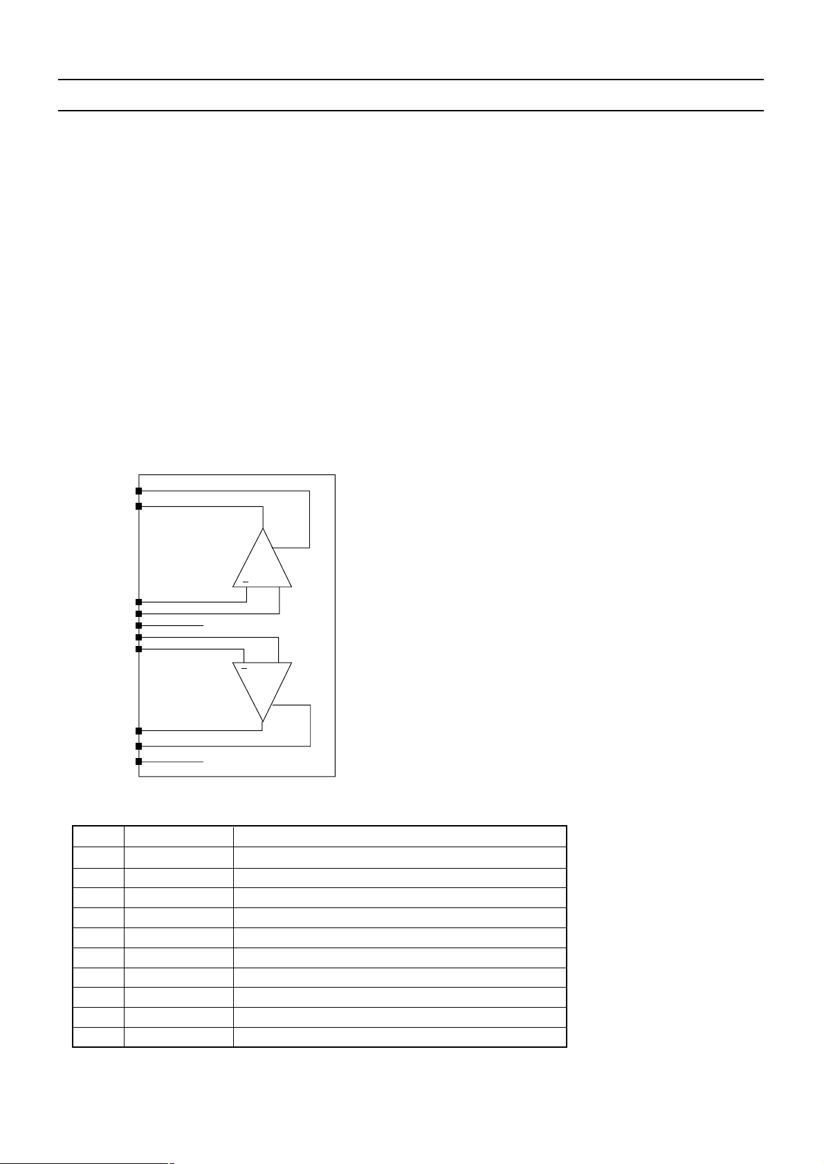
Service manual SC-150
-42-
4-11 LA6515
4-11-1 General description
The LA6515 features an on-chip current limiter and provides high voltage gain and a high common-mode
rejection ratio.
The LA6515 is an ideal choice for power applications such as DC servos, capstan drivers, actuator drivers,
programmable power supplies and high-quality audio amplifiers.
The LA6515 is available in 10-pin SIPs and operates from -15V and 15V supplies.
4-11-2 Features
-0.5A output current
-100dB voltage gain
-80dB common-mode rejection
-0.15V/us slew rate
4-11-3 Block diagram
-2mV offset voltage
-10nA offset current
-On-chip current limiter
-15V and 15V supplies
4-11-4 Pin Description
Pin Symbol Description
1
2
3
4
5
6
7
8
9
10
VSENSE1
OUT1
V1-
V1+
VEE
V2+
V2-
OUT2
VSENSE2
Vcc
Voltage detect
Output
Inverting input
Non-inverting input
-15V supply
Non-inverting input
Inverting input
Output
Voltage detect
15V supply
VSENSE1
VOUT1
VOUT2
VSENSE2
VCC
VIN1-
VIN1+
VEE
VIN2+
VIN2-
+
+
Page 44
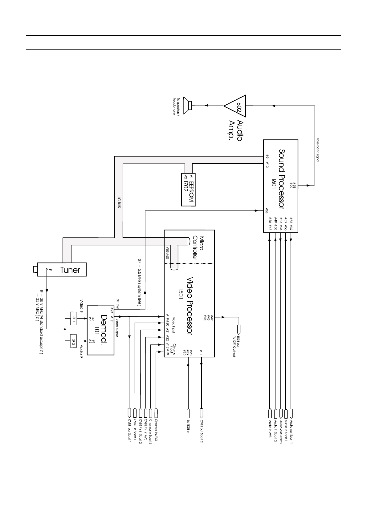
Service manual SC-150
-43-
5 - Circuit description
5-1 Block diagram
Page 45
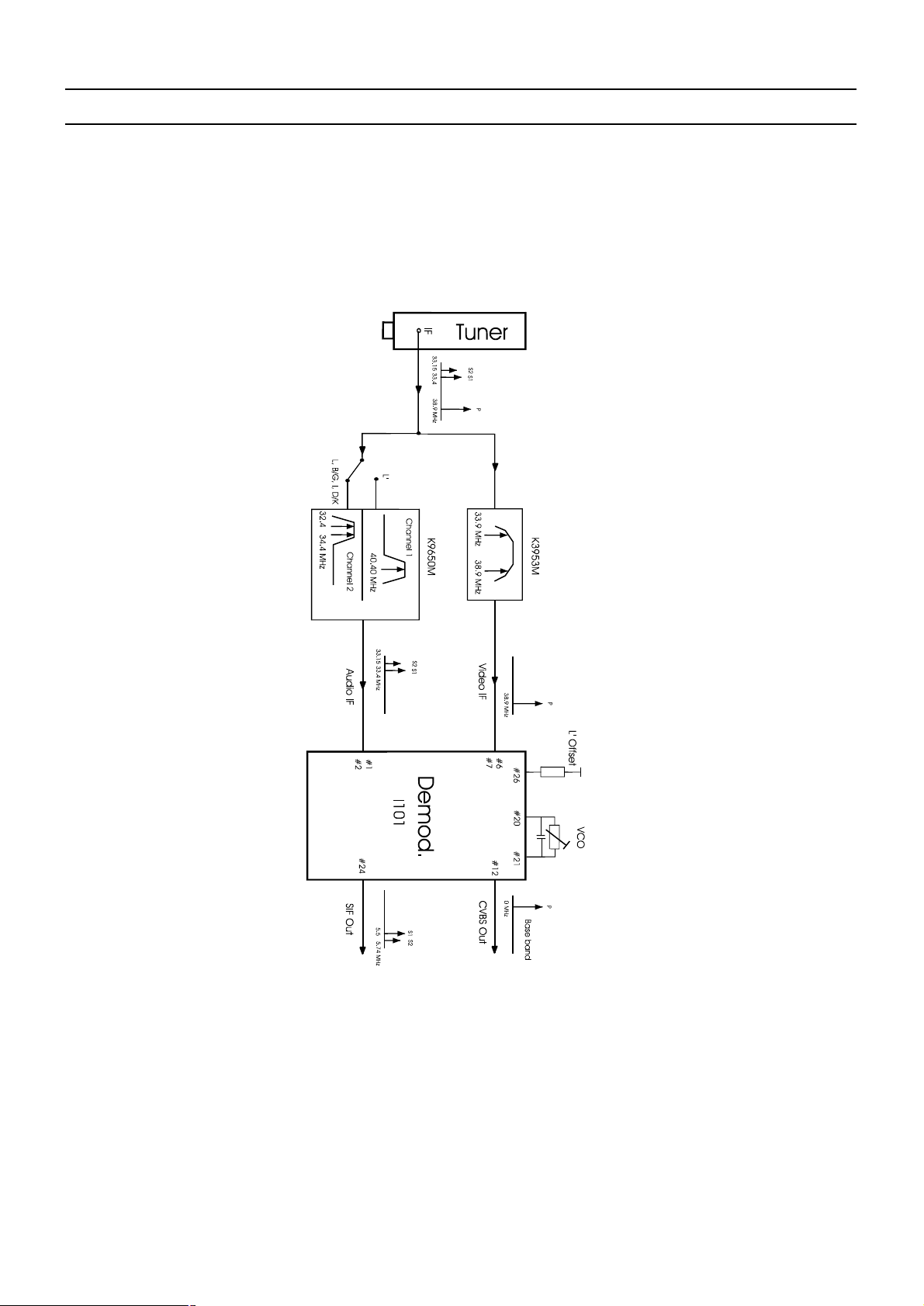
Service manual SC-150
-44-
5-2 IF section
5-2-1 Block diagram
The video IF signal (VIF) is fed through a SAW filter to the differential input (Pin 6-7) of the VIF amplifier.
5-2-2 Vision IF Amplifier
This amplifier consists of three AC-coupled amplifier stages. Each differential amplifier is gain controlled by the
automatic gain control circuit (VIF-AGC). The output signal of the VIF amplifier is applied to the FPLL carrier
generation and the video demodulator.
Page 46

Service manual SC-150
-45-
SAW filters
Ref. Standard Features
K3953M B/G - D/K - I - L/L’ - IF filter for video application
- TV IF filter with Nyquist slopes at 33.9 MHz and
38.9 MHz
- Constant group delay
K9650M B/G - D/K - I - L/L’ - IF filter for audio application
- TV IF audio filter with two channels
- Channel 1 (L’ ) with one pass band for sound
carrier at 40.40 MHz
- Channel 2 ( L, D/K, I, B/G) with one pass band for
sound carriers between 32.40 MHz and 33.40 MHz
5-2-3 Tuner-and VIF-AGC
At Pin 8, the VIF-AGC charges/discharges the AGC capacitor to generate a control Voltage for setting the gain of the
VIF amplifier and tuner in order to keep the video output signal at a constant level. Therefore, in the case of all
negative modulated signals (e.g., B/G standard) the sync. level of the demodulated video signal is the criterion for a
fast charge/discharge of the AGC capacitor. For positive modulation (e.g., L standard) the peak white level of video
signal controls the charge current. In order to reduce reaction time for positive modulation, where a large time constant
is needed, an additional black level detector controls the discharge current in the event of decreasing VIF input signal.
The control voltage (AGC voltage at Pin 8) is transferred to an internal control signal, and is fed to the tuner AGC to
generate the tuner AGC current at Pin 11 (open collector output). The take over point of the tuner AGC can be adjusted
at Pin 10 by a potentiometer or an external dc voltage (from interface circuit or microprocessor).
5-2-4 FPLL, VCO and AFC
The FPLL circuit (frequency phase locked loop) consists of a frequency and phase detector to generate the control
voltage for the VCO tuning. In locked mode, the VCO is controlled by the phase detector and in unlocked mode,
the frequency detector is superimposed. The VCO operates with an external resonance circuit (L and C parallel) and is
controlled by internal varicaps. The VCO control voltage is also converted to a current and represents the AFC output
signal at Pin 22. At the AFC switch (Pin 19) three operating conditions of the AFC are possible:
AFC curve “rising” or “falling” an d AFC “off”. A practicable VCO alignment of the external coil is the adjustment to
zero AFC output current at Pin 22. At center frequency the AFC output current is equal to zero. Furthermore, at Pin
14, the VCO center frequency can be switched for setting to the required L’ value (L’ standard). The optional
potentiometer at Pin 26 allows an offset compensation of the VCO phase for improved sound quality (fine adjustment).
Without a potentiometer (open circuit at Pin 26), this offset compensation is not active. The oscillator signal passes a
phase shifter and supplies the in-phase signal (0
o
) and the quadrature signal (90o) of the generated picture carrier.
Page 47

Service manual SC-150
-46-
5-2-5 Video Demodulation and Amplifier
The video IF signal, which is applied from the gain controlled IF amplifier, is multiplied with the in-phase component
of the VCO signal. The video demodulator is designed for low distortion and large bandwidth. The demodulator output
signal passes an integrated low pass filter for attenuation of the residual vision carrier and is fed to the video amplifier.
The video amplifier is realised by an operational amplifier with internal feedback and 8 MHz bandwidth (–3 dB). A
standard dependent dc level shift in this stage delivers the same sync. level for positive and negative modulation. A n
additional noise clipping is provided. The video signal is fed to VIF-AGC and to the video output buffer. This amplifier
with a 6 dB gain offers easy adaptation of the sound trap. For nominal video IF modulation the video output signal at
Pin 12 is 2 Vpp.
5-2-6 Sound IF Amplifier and SIF-AGC
The SIF amplifier is nearly identical with the 3-stage VIF amplifier. Only the first amplifier stage exists twice and is
switchable by a control voltage at Pin 3. Therefore with minimal external expense it is possible to switch between two
different SAW filters. Both SIF inputs features excellent cross-talk attenuation and an input impedance which is
independent from the switching condition. The SIF-AGC is related to the average level of AM- or FM-carrier and
controls the SIF amplifier to provide a constant SIF signal to the AM demodulator and QPS mixer.
5-2-7 Quasi-Parallel-Sound (QPS) Mixer
The QPS mixer is realised by a multiplier. The SIF signal (FM or NICAM carrier) is converted to the intercarrier
frequency by the regenerated picture carrier (quadrature signal) which is provided from the VCO. The intercarrier
signal is fed via an output amplifier to Pin 24.
5-2-8 Standard Switch
To have equal polarity of the video output signal the polarity can be switched in the demodulation stage in accordance
with the TV standard. Additionally a standard dependent dc level shift in the video amplifier delivers the same sync. level.
In parallel to this, the correct VIF-AGC is selected for positive or negative modulated VIF signals. In the case of
negative modulation (e.g., B/G standard) the AM output signal is switched off. For positive modulation (L standard) the
AM demodulator and QPS mixer is active. This condition allows a parallel operation of the AM sound signal and the
NICAM-L stereo sound.
5-2-9 L’ Switch
With a control voltage at Pin 14 the VCO frequency can be switched for setting to the required L’ value (L’ standard).
Also a fine adjustment of the L’-VCO center frequency is possible via a potentiometer. The L’ switch is only active for
positive modulated video IF-signals (standard switch in L mode).
5-2-10 Internal Voltage Stabiliser
The internal bandgap reference ensures constant performance independent of supply voltage and temperature.
Page 48

Service manual SC-150
-47-
5-3 V ideo - VCT description
5-3-1 Introduction
The VCT 38xxA includes complete video, display, and deflection processing.
All processing is done digitally, the video front-end and video back-end are interfacing to the analogue world.
Most functions can be controlled by software via I 2 C bus slave interface.
5-3-2 V ideo Front-end
This block provides the analogue interfaces to all video inputs and mainly carries out analogue-to-digital conversion for
the following digital video processing. Most of the functional blocks in the front-end are digitally controlled (clamping,
AGC, and clock-DCO). The control loops are closed by the Fast Processor (‘FP’) embedded in the video decoder.
5-3-3 Input Selector
Up to seven analogue inputs can be connected. Four inputs are for input of composite video or S-VHS luma signal.
These inputs are clamped to the sync back porch and are amplified by a variable gain amplifier. Two chroma inputs can
be used for connection of S-VHS carrier-chrominance signal. These inputs are internally biased and have a fixed gain
amplifier.
5-3-4 Clamping
The composite video input signals are AC-coupled to the IC. The clamping voltage is stored on the coupling capacitors
and is generated by digitally controlled current sources. The clamping level is the back porch of the video signal.
S-VHS chrominance is also AC-coupled. The input pin is internally biased to the center of the ADC input range. Each
channel is sampled at 10.125 MHz with a resolution of 8 bit.
5-3-5 Automatic Gain Control
A digitally working automatic gain control adjusts the
magnitude of the selected baseband.
5-3-6 Digitally Controlled Clock Oscillator
The clock generation is also a part of the analogue front-end. The crystal oscillator is controlled digitally by the control
processor. The clock frequency can be adjusted within ±150 ppm. This adjustment is done in factory for every TV set.
5-3-7 Analogue V ideo Output
The input signal of the Luma ADC is available at the analogue video output pin (#11). The signal at this pin is buffered
by a source follower. The output voltage is 2 V. The magnitude is adjusted with an AGC in 8 steps together with the
main AGC.
Page 49

Service manual SC-150
-48-
5-3-8 Adaptive Comb Filter (VCT3834A only)
The adaptive comb filter is used for high-quality luminance/chrominance separation for PAL or NTSC signals. The
comb filter improves the luminance resolution (bandwidth) and reduces interferences like cross-luminance and
cross-color artefacts. The adaptive algorithm can eliminate most of the mentioned errors without introducing new
artefacts or noise. The filter uses two line delays to process the information of three adjacent video lines. To have a
fixed phase relationship of the colour subcarrier in the three channels, the system clock (20.25 MHz) is fractionally
locked to the colour subcarrier. This allows the processing of all colour standards and substandards using a single
crystal frequency. The CVBS signal in the three channels is filtered at the subcarrier frequency by a set of bandpass/
notch filters. The output of the three channels is used by the adaptation logic to select the weighting that is used to
reconstruct the luminance/chrominance signal from the 4 bandpass/notch filter signals. By using soft mixing of the 4
signals switching artefacts of the adaption algorithm are completely suppressed. The comb filter uses the middle line as
reference, therefore, the comb filter delay is one line. If the comb filter is switched off, the delay lines are used to pass
the luma/ chroma signals from the A/D converters to the luma/ chroma outputs. Thus, the comb filter delay is always
one line.
5-3-9 Color Decoder
In this block, the standard luma/chroma separation and multi-standard colour demodulation is carried out. The colour
demodulation uses an asynchronous clock, thus allowing a unified architecture for all colour standards.
The colour killer uses the burst-phase/ burst-frequency measurement to identify a PAL/NTSC or SECAM colour signal.
For PAL/NTSC, the colour is s witched off (killed) as long as the colour subcarrier PLL is not locked. For SECAM, the
killer is controlled by the toggle of the burst frequency. The burst amplitude measurement is used to switch-off the
colour if the burst amplitude is below a programmable threshold. Thus, colour will be killed for very noisy signals.
The colour amplitude killer has a programmable hysteresis.
The burst-frequency measurement is also used for automatic standard recognition (together with the status of horizontal
and vertical locking) thus allowing a completely independent search of the line and colour standard of the input signal.
The following standards can be distinguished:
PAL B,G,H,I; NTSC M; SECAM; NTSC 44; PAL M; PAL N; PAL 60. In AV mode or when Prg No 0 is selected all the
standards above are enabled by the controlling software. In INSTALL menu the controlling software enables PAL B,G,
H,I and SECAM detection. The colour standard for each program number is stored in EEPROM. Outside INSTA LL
menu and for programmes numbers 1 to 99, the auto colour detection is disabled, the colour standard is recall from
EEPROM and forced.
5-3-10 Horizontal Scaler (VCT3834A only)
The 4:2:2 YC r C b signal from the colour decoder is processed by the horizontal scaler. The scaler block allows a
linear or nonlinear horizontal scaling of the input video signal in the range of 0.25 to 4. Nonlinear scaling, also called
“Panoramavision”, provides a geometrical distortion of the input picture. It is used to fit a picture with 4:3 format on a
16:9 screen by stretching the picture geometry at the borders. Also, the inverse effect can be produced by the scaler.
The scaler contains a programmable decimation filter, a 1-line FIFO memory, and a programmable interpolation filter.
Page 50

Service manual SC-150
-49-
5-3-11 Video Sync Processing
To extract the sync information from the video signal, a linear phase low-pass filter eliminates all noise and video
contents above 1 MHz. The sync is separated by a slicer; the sync phase is measured. A variable window can be
selected to improve the noise immunity of the slicer. The phase comparator measures the falling edge of sync, as well
as the integrated sync pulse. The sync phase error is filtered by a phase-locked loop that is computed by the Fast
Processor. All timing in the front-end is derived from a counter that is part of this PLL, and it thus counts synchronously to the video signal. A separate hardware block measures the signal back porch and also allows gathering the
maximum/minimum of the video signal. This information is processed by the FP and used for gain control and
clamping. For vertical sync separation, the sliced video signal is integrated. The FP uses the integrator value to derive
vertical sync and field information. The information extracted by the video sync processing is multiplexed onto the
hardware front sync signal (FSY) and is distributed to the rest of the video processing system.
The data for the vertical deflection, the sawtooth, and the East-West correction signal is calculated by the VCT 38xxA.
5-3-12 Display Processing
In the display processing the conversion from digital YC r C b to analogue RGB is carried out.
In the luminance processing path, contrast and brightness adjustments and a variety of features, such as black-level
expansion, dynamic peaking and soft limiting, are provided. In the chrominance path, the C r C b signals are converted
to 4:4:4 format and filtered by a colour transient improvement circuit. The YC r C b signals are converted by a programmable matrix to RGB colour space. The digital OSD insertion circuit allows the insertion of a 5-bit OSD signal.
The OSD signals and the display clock are synchronised to the horizontal flyback.
5-3-13 Chroma Transient Improvement
The intention of this block is to enhance the chroma resolution. A correction signal is calculated by differentiation of
the colour difference signals. The differentiation can be selected according to the signal bandwidth, e.g. for PAL/NTSC/
SECAM or digital component signals, respectively. The amplitude of the correction signal is adjustable. Small noise
amplitudes in the correction signal are suppressed by an adjustable coring circuit. To elimina te ‘wrong colours’, which
are caused by over and undershoots at the chroma transition, the sharpened chroma signals are limited to a proper value
automatically.
5-3-14 Video Back-end
The digital RGB signals are converted to analogue RGBs using three video digital-to-analogue converters (DAC) with
10-bit resolution. An analogue brightness value is provided by three additional DACs. The adjustment range is 40 % of
the full RGB range. Controlling the white-drive/analogue brightness and also the external contrast and brightness
adjustments is done via the Fast Processor, located in the front-end. Control of the cutoff DACs is done via I 2 C bus
registers. Finally cutoff and blanking values are added to the RGB signals. Cutoff (dark current) is provided by three 9bit DACs. The adjustment range is 60 % of full scale RGB range. The analogue RGB-outputs are current outputs with
current-sink characteristics. The maximum current drawn by the output stage is obtained with peak white RGB. An
external half contrast signal can be used to reduce the output current of the RGB outputs to 50% . Cutoff and whitedrive current measurement are carried out during the vertical blanking interval. They always use the small bandwidth
setting.
Page 51

Service manual SC-150
-50-
5-3-15 CRT Measurement and Control
The display processor is equipped with an 8-bit ADC for all measuring purposes. The ADC is connected to the
SENSE input pin. Cutoff and white-drive current measurement are carried out during the vertical blanking interval.
5-3-16 Average Beam Current Limiter
The average beam current limiter (BCL) uses the SENSE input for the beam current measurement. The BCL uses a
different filter to average the beam current during the active picture. The filter bandwidth is approx. 2 kHz. The beam
current limiter has an automatic offset adjustment that is active two lines before the first cutoff measurement line. The
beam current limiter function is located in the front-end. The data exchange between the front-end and the back-end is
done via a single-wire serial interface. The beam current limiter allows the setting of a thresh-old current. If the beam
current is above the threshold, the excess current is low-pass filtered and used to attenuate the RGB outputs by
adjusting the white-drive multipliers for the internal (digital) RGB signals, and the analogue contrast multipliers for the
analogue RGB inputs, respectively. The lower limit of the attenuator is programmable, thus a minimum contrast can
always be set. During the tube measurement, the ABL attenuation is switched off. After the white-drive measurement
line it takes 3 lines to switch back to BCL limited drives and brightness.
5-3-17 Analogue RGB Insertion
The VCT 38xxA allows insertion of external analogue RGB signals. The RGB signal is key-clamped and inserted into
the main RGB by the Fast-Blank switch. The external RGB input can be overlaid or underlaid to the digital picture.
The external RGB signals can be adjusted independently as regards DC level (brightness) and magnitude (contrast). All
signals for analogue RGB insertion (RIN, GIN, BIN, FBLIN) must be synchronised to the horizontal flyback, otherwise a horizontal jitter will be visible. The VCT 38xxA has no means for timing correction of the analogue RGB input
signals. RGB signals are not digitalised and therefore cannot be processed by the picture scaler.
5-3-18 Fast-Blank Monitor
The presence of external analog RGB sources can be detected by means of a Fast-Blank monitor. With a special
monitor logic it is possible to detect if there is an external RGB source active and if it is a full screen insertion or only
a box. The monitor logic is connected directly to the FBLIN pin. The controlling software uses this information to
disable all picture format using display scaler.
5-3-19 Vertical and East/West Deflection
The calculations of the vertical and East/West deflection waveforms is done by the internal Fast Processor (FP).
The algorithm uses a chain of accumulators to generate the required polynomial waveforms. To produce the deflection
waveforms, the accumulators are initialised at the beginning of each field. The initialisation values must be computed
by the TV control processor and ar
e written to the front-end once.
Page 52

Service manual SC-150
-51-
5-3-20 EHT Compensation
The vertical waveform can be scaled according to the average beam current. This is used to compensate the effects of
electric high-tension changes due to beam current variations. EHT compensation for East/West deflection is done with
an offset corresponding to the average beam current.
5-3-21 Reset Function
Reset of all VDP functions is performed by the RESQ pin. When this pin becomes active, all internal registers and
counters are lost.
5-3-22 Standby and Power-On
The VDP does not have a standby mode. To disable all the analogue and digital video functions, it is necessary to
switch off the supplies for analogue front-end (VSUP AF ), analogue back-end (VSUP AB ) and digital circuitry
(VSUP D ).
5-4- Microcontroller
5-4-1 Introduction
The TV controller basically consists of the CPU, RAM, ROM, and a number of peripheral modules.
For instance:
– a memory banking module is included to allow access to more than 64 kB memory.
– a bootloader softwa re is included to allow in-system-downloading of external code to Flash memory via the I 2 C
interface.
The TV controller runs the complete software necessary to control a TV set. The software includes control of the audio,
video, OSD, and text processors on chip, as well, as control of external devices like tuner or stereo decoder.
Communication between the TV controller and external devices is done either via I 2 C bus interface or via programmable port pins. The TV Controller is clocked with f OSC = f XTAL /2.
5-4-2 CPU
The CPU is fully compatible to WDC’s W65C02 micro-processor. The processor has 8-bit registers/accumulator, an 8-
bit data bus, and a 16-bit address bus.
Page 53
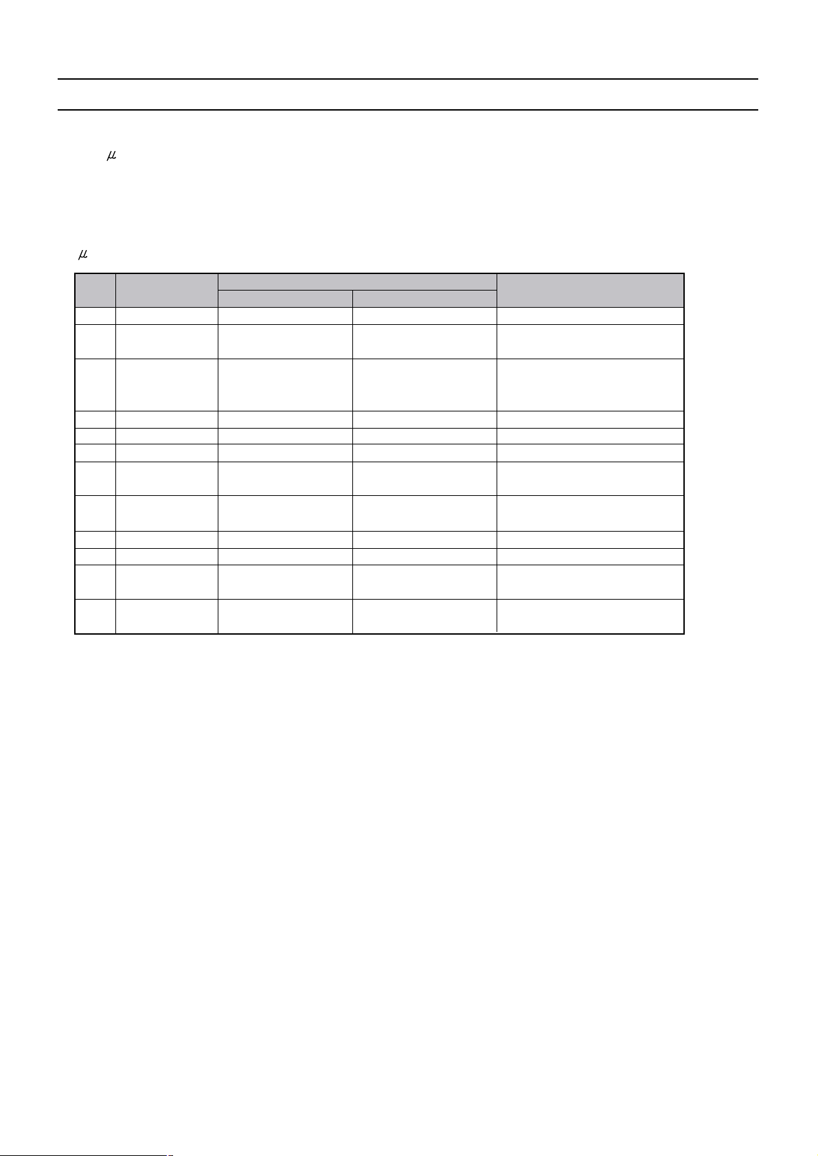
Service manual SC-150
-52-
configuration
Stand by TV ON
1 Power Push Pull Low Push Pull High Switch OFF / ON SMPS
2 AGC High impedance High impedance Tuner AGC level input –
For factory use only
5 Mod SW High impedance Push Pull High = Negative
modulation, Low = Positive
modulation (L/L’).
6 SECAM L’ High impedance Push Pull Low = L, High =L’
7 AFC High impedance High impedance ADC input
8 IR High impedance High impedance Interrupt input
9 SC1 SW High impedance High impedance SCART 1 slow switching –
ADC input
10 SC2 SW High impedance High impedance SCART 2 slow switching –
ADC input
61 Mute Push Pull Push Pull High = Mute active
62 LED Open Drain Open Drain
63 K B High impedance High impedance Keyboard input – ADC
input
64 OC P High impedance High impedance Over Current Protection –
Switch the set to Std by if < 2.
5-4-3 - Controller I/O pin configuration and function
There exist different kinds of ports. The universal ports serv
e as digital I/O and have additional special input and output
functions. A subset of the universal ports serves as input for the analogue-to-digital converter.
- Controller I/O pin configuration and function table
pin
name
description
To reduce power consumption in stand by mode all ports not used are configured in high impedance mode.
5-4-4 Tuning
The AFC information is supplied by the demodulator IC, and becomes available on VCT pin 7 for controlling software.
The controlling software uses this information for tuner frequency tracking ( automatic following ). The AFC window
is typically between 50 KHz and 100 KHz.
The minimum frequency step of the tuner is 50 Khz.
This AFC function is disabled when a program is tuned using the direct frequency entry or after fine tuning adjustment.
Therefore it is recommended to tune channel with the TV search function ( manual or ATSS ) or using the direct
channel entry to enable the Automatic Frequency Control.
5-4-5 Automatic Format switching and WSS
When AUTO mode is selected by the user, the television will automatically select a mode for the user. The format
information is supplied
by SCART pin 8 level when in AV mode or by WSS data. The signal contains codes as defined in
the WSS European Telecommunication Standard, ETS 300 294. Briefly, the signal is received at the beginning of line
Page 54

Service manual SC-150
-53-
Format Zoom factor – TV with Description Application
Name(OSD) 16:9 CRT
Vertical Horizontal
4:3 100% 75% Picture is centred with Standard 4/3 picture with
black bars at the left 576 active lines
and right hand side of
the display
14:9 114% 87% Picture is centred with 14:9 picture – letter box
black bars at the left format with 504 active
and right hand side of lines
the display
ZOOM 14:9 114% 100% Picture is displayed 14:9 picture – letter box
filling the full width of the format with 504 active
screen by incorporating lines
a small horizontal
geometrical error
(typically 8% linear)
ZOOM 16:9 133% 100% Picture is displayed 16:9 picture – letter box
filling the full screen format with 430 active
(width and height) lines
PANORAMA 100% 100% Picture is displayed Used to fit a picture with
filling the full screen 4:3 format on a 16:9
(width and height) screen by stretching the
picture geometry at the
borders.
23, in each frame. This is bi-phase encoded using a clock frequency of 5 MHz. In total, 14 data bits are available, in
4 groups. Group 1 contains the codes for the received format.
The mode chosen is defined by the following table. In effect the default mode is full screen.
The table below gives a summary of the FORMAT modes available (for WP895 and WP895F), and their given
properties.
Page 55
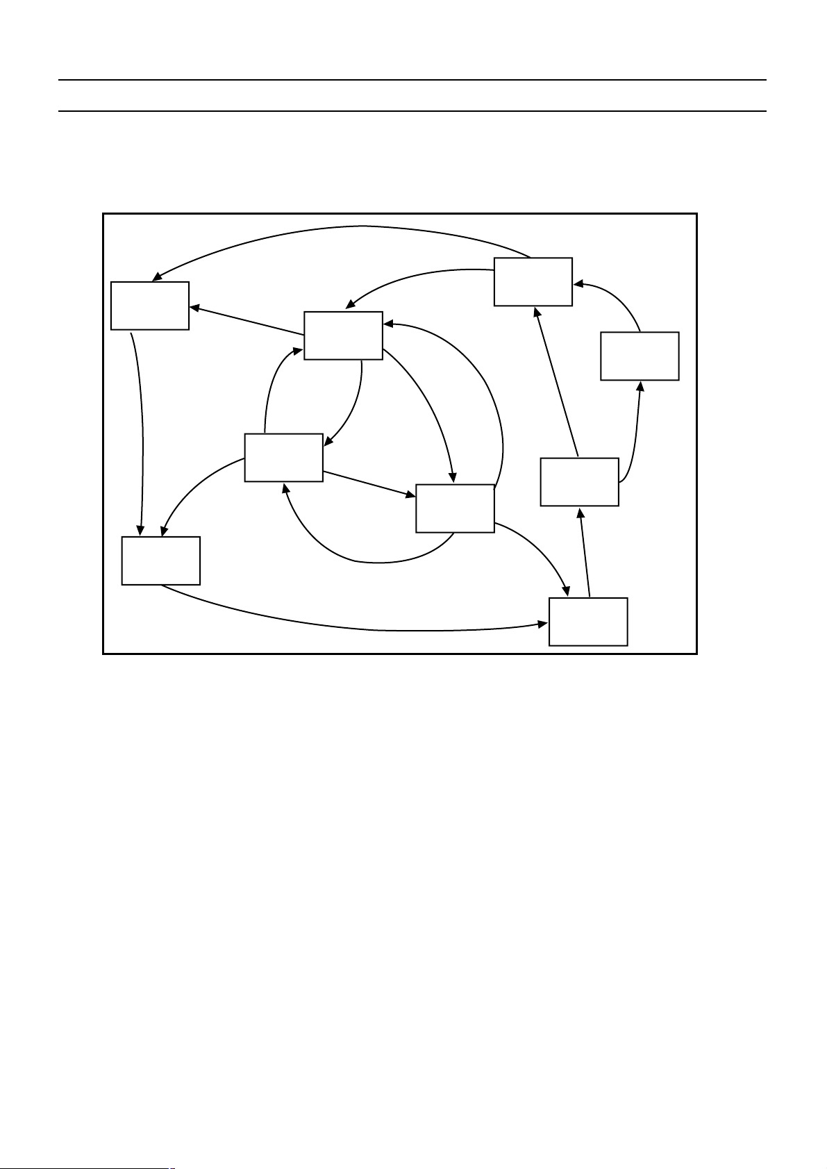
Service manual SC-150
-54-
The following schematic, illustrates the logic of control for the two SCART connectors.
The terms used in the schematic are described below ;
1. AUTO represents a situation where the television has self-selected its picture source. This could be when the
SCART SLOW SWITCHING pin has gone to a high state, and the AV 1 input is selected without the intervention
of the user.
2. FORCED represents the change of source which has been commanded by the user (using the EXTERNAL button).
The user always has priority, and can override the AUTO change of source by the television.
3. AV KEY represents the EXTERNAL button of the remote control, or on the television.
4. S/SW 1, or S/SW 2 represent the SLOW SWITCHING inputs of the first SCART (AV 1) or second SCART (AV
2), these each being pin number 8.
5. F/SW 1 represents the FAST SWITCHING input of the first SCART (AV 1), on pin number 16. The second
SCART, AV 2, input does not possess a FAST SWITCHING input.
The HIGH state of a slow switching input represents the request from the external source to be selected by the
television. Whether this is accepted or not depends on the position in the logic diagram. The general rule is that the user
always has priority, so the use of the AV KEY will always result in a defined logic path being followed.
Under certain circumstances, defined in the diagram, the change of state of a slow switching input will result in the
automatic change of source by the television. This change, such as the change from RF broadcast to the AV 1 input,
5-4-6 EXTERNAL source control logic
FORCED
AV 1
FORCED
AV 2
FORCED
S-VHS2
FORCED
S-VHS3
FORCED
AV3
FORCED
RF
AUTO
RF
AUTO
AV 1
AUTO
AV 2
AV KEY
AV KEY
AV KEY
AV KEY
AV KEY
AV KEY
ENABLE F/SW 1
ENABLE
F/SW 1
ENABLE
F/SW 1
ENABLE
F/SW 1
AV
KEY
AV
KEY
AV
KEY
AV
KEY
DISABLE
F/SW 1
DISABLE
F/SW 1
DISABLE
F/SW 1
DISABLE
F/SW 1
S/SW 1 LOW &
S/SW 2 LOW
S/SW 1 LOW
& S/SW 2 LOW
S/SW 1 LOW &
S/SW 2 LOW
S/SW 1
HIGH
S/SW 1
HIGH
S/SW 1
HIGH
S/SW 2
HIGH
OPTION
WP895
Page 56

Service manual SC-150
-55-
can always be overridden by the user after the event.
Each line on the diagram, with its associated text, represents the exact conditions under which the change of state will
occur. Sometimes this will be accompanied by another action which will be automatically performed by the television,
being to either ENABLE or DISABLE F/SW 1.
5-4-7 Over Current Protection
In case of overload, the SMPS secondary voltages will drop. The voltage on pin 64 of microcontroller drops below a
reference voltage (2.26V). The controlling software which continuously monitors this voltage will switch the set to
stand by mode. To power on the set again the user must switch it off using the main power switch. Appropriate hysteresis guaranrees a reliable operation.
5-5 Teletext Display
National character option bits C12, C13, C14 are transmitted in the page header of a given teletext page. The national
option bits are intended to change (or exchange) 13 characters within the G0 character set, according to the needs of
each national language. However, for Cyrillic and Greek languages, a major character set change (a change of character
mapping) needs to effected for correct display.
These codes represent, for a given broadcaster, the intended language that the teletext page should be displayed in. As
there are only 3 bits, there are only 8 codes available to cover all the possible language combinations. This means that
for a received code there are several possibilities meanings, and therefore several possibilities for display.
This is not as bad as it first seems, as we use the user-selected OSD language to identify the intention of the broadcaster.
For example, a user wishing to see Russian teletext should select Russian OSD language, otherwise he would not have
correct teletext display on the TV.
The table below allows the reader to understand the relationship between selected OSD language (which is under user
control), the teletext language display (selected by national option bits in transmission page header) and the language
mapping (either Latin or Greek/Cyrillic)
An example: For Greek teletext display, (if national option code 1 1 1 is received from the broadcaster), the user should
select the Greek OSD language. Even if English, French, German, Italian, Spanish, Dutch, Danish, Finnish, Norwegian
or Swedish OSD languages are selected, the teletext will be correctly displayed.
However, if Polish, Hungarian, Czech, Slovakian, Rumanian or Russian OSD are selected, Latin font mapping is
selected. The consequence will be incorrect teletext display, with NO GREEK CHARACTERS DISPLAYED. Romanian national font options will be selected.
Page 57
Service manual SC-150
-56-
OSD Language C C C Teletext Language ESC Mapping
12 13 1 4 Teletext Language
0 0 0 English English Latin
0 0 1 German German Latin
0 1 0 Swedish/Finnish Swedish/Finnish Latin
0 1 1 Italian Italian Latin
1 0 0 French French Latin
1 0 1 Spanish Spanish Latin
1 1 0 Turkish Turkish Latin
1 1 1 English Greek Greek/Cyrillic
0 0 0 Polish Polish Latin
0 0 1 German German Latin
0 1 0 Hungarian Hungarian Latin
0 1 1 Italian Italian Latin
1 0 0 French French Latin
1 0 1 Serb/Croat/Slovenian Serb/Croat/Slovenian Latin
1 1 0 Czech/Slovak Czech/Slovak Latin
1 1 1 Rumanian Rumanian Latin Russian
0 0 0 English Serbian/Montenegrin Greek/Cyrillic
0 0 1 German German Latin
0 1 0 Estonian Estonian Latin
0 1 1 Lettish/Lithuanian Lettish/Lithuanian Latin
1 0 0 English Russian/Bulgarian Greek/Cyrillic
1 0 1 English Ukrainian Greek/Cyrillic
1 1 0 Czech/Slovak Czech/Slovak Latin
1 1 1 Rumanian Rumanian Latin
English, French,
German, Italian,
Spanish, Dutch,
Danish, Finnish,
Norwegian,
Swedish, Greek
Polish,
Hungarian,
Czech,
Slovakian,
Rumanial
Russian
Bulgarian
5-6 Sound processing
5-6-1 Analogue sound IF - input section
The input pins ANA_IN1+ and ANA_IN- offer the possibility to connect sound IF sources to the MSP 341xD. The
analogue-to-digital conversion of the preselected sound IF signal is done by an A/D converter, whose output is used to
control an analogue automatic gain circuit (AGC), providing an optimal level for a wide range of input levels.
5-6-2 Quadrature Mixers
The digital input coming from the integrated A/D converter may contain audio information at a frequency range of
theoretically 0 to 9 MHz corresponding to the selected standards. By means of two programmable quadrature mixers,
two different audio sources ; for example, NICAM and FM-mono, may be shifted into baseband position.
5-6-3 Phase and AM discrimination
The filtered sound IF signals are demodulated by means of the phase and amplitude discriminator block. On the output,
the phase and amplitude is available for further processing.
AM signals are derived from the amplitude information, whereas the phase information serves for FM and NICAM
demodulation.
Page 58

Service manual SC-150
-57-
5-6-4 NICAM decoder
In case of NICAM - mode, the phase samples are decoded according the DQPSK - coding scheme. The output of this
block contains the original NICAM bitstream.
5-6-5 DSP section
All audio baseband functions are performed by digital signal processing (DSP). The DSP section controls the source
and output selection, and the signals processing.
5-6-6 Sound Mode switching
In case of NICAM transmission, the controlling software reads the bit error r
ate and the operation mode from the
NICAM Decoder. When the set is in “Auto detection” mode ( default mode after ATSS ) the controlling software sets
automatically the sound mode ( NICAM mono, NICAM Dual 1 or NICAM Dual 2 ) depending on the transmitted
mode.
In the case of 2 Carrier FM transmission, the contr
olling software read the transmission mode and the signal quality level
from the Stereo Detection Register. When the set is in “Auto detection” mode the controlling software automatically sets
the sound mode ( mono, Stereo, Dual 1, Dual 2 ) depending on the transmitted mode.
In “Auto detection” mode the controlling software evaluates the signal quality and automatically switches to the analogue
sound carrier 1, if the transmission quality is too poor. To avoid unwanted automatic switching the threshold levels
mono to stereo and stereo to mono are dif
ferent.
In “forced mono “ mode ( Red OSD in status Display Window),
the controlling software configures the MSP341xD to
demodulate onl
y the analogue (FM or AM) sound carrier 1, no matter the signal quality. The sound mode “ forced “ or “
Autodetect” is stored for each programme.
5-7 Sound amplification
The TDA8946J is a stereo BTL audio amplifier capable of delivering 2 x 15 W output power to
an 8 W load at THD = 10%, using a 18 V power supply and an external heatsink. The voltage gain is fixed at 32dB.
With the three-level MODE input the device can be switched from ‘standby’ to ‘mute’ and to ‘operating’ mode.
The TDA 8946J outputs are protected by an internal thermal shutdown protection mechanism and short-circuit
protection.
5-7-1 Power amplifier
The power amplifier is a Bridge Tied Load (BTL) amplifier with an all-NPN output stage, capable of delivering a peak
output current of 1.5 A.
The BTL principle offers the following advantages :
- Lower peak value of the supply current.
- The ripple frequency on the supply voltage is twice the signal frequency.
- No DC-blocking capacitor
- Good low frequency performance
Page 59

Service manual SC-150
-58-
5-7-2 Mode selection
The TDA894xJ has several functional modes, which can be selected by applying the proper DC voltage to pin MODE.
Mute : In this mode the amplifier is DC biased but not operational (no audio output). This allows the input coupling
capacitors to be charged to avoid pop-noise. The device is in mute mode when 2.5 V <
V
MODE
< (Vcc-1.5 V).
Operating : In this mode the amplifier is operating normally. The operating mode is activated at V
MODE
< 0.5 V.
5-8 Vertical deflection
The vertical driver circuit is a bridge configuration. The deflection coil is connected between the output amplifiers,
which are driven in phase opposition. The differential input circuit is voltage driven. The input circuit is especially
intended for direct connection to driver circuits which deliver symmetrical current signals, but is also suitable for
asymmetrical currents. The output current of these devices is converted to voltages at the input pins via resistors R350
and R351. The differential input voltage is compared with the output current through the deflection coils measured as
voltage across R398, which provides internal feedback information. The voltage across R398 is proportional to the
output current.
5-8-1 Flyback voltage
The flyback voltage is determined by an additional supply voltage V
flb
. The principle of operation with two supply
voltages (class G) makes it possible to fix the supply voltage Vp optimum for the scan voltage and the second supply
voltage V
flb
optimum for the flyback voltage. Using this method, very high efficiency is achieved. The supply voltage
V
flb
is almost totally available as flyback voltage across the coil, this being possible due to the absence of a coupling
capacitor.
5-8-2 Protection
The output circuit has protection circuits for :
- Too high die temperature
- overvoltage of output stage A
5-8-3 Guard circuit
The guard signal
is not used.
5-8-4 Damping resistor
For HF loop stability a damping resistor (R331) is connected across the deflection coil.
5-8-5 EAST-WEST Amplifier (TDA8358J)
The East-West amplifier is current driven. It can only sink currents of the diode modulator circuit. A feedback resistor
R397 is connected between the input and output of this inverting amplifier in order to convert the East-West cor rection
input into an output voltage.
Page 60
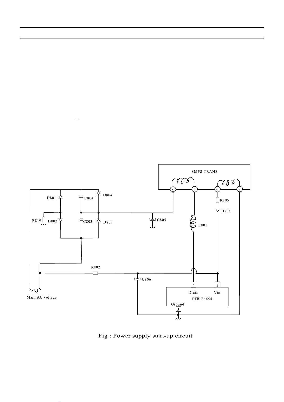
Service manual SC-150
-59-
5-9 Power supply (STR F6654)
5-9-1 STR-F6654 general description
The STR-F6654 is an hybrid IC with a build-in MOSFET and control IC, designed for flyback converter type switch
mode power supply applications.
5-9-2 Power supply primary par t operations
An oscillator generates pulses signals which turn on and off a MOSFET transistor.
5-9-2-1 Start-up circuit : V
IN
The start-up circuit is used to start and stop the operation of the control IC, by detecting a voltage appearing at V
IN
pin (pin 4).
Page 61

Service manual SC-150
-60-
When the power switch is pushed on, VIN increases slowly. During this time, C806 is charged through R802.
As soon as VIN reaches 16V, the STR-F6654 control circuit starts operating. Then, VIN is obtained by smoothing the
winding voltage which appears between pin6 and pin7 of the SMPS transformer.
As this winding voltage does not increase to the set voltage immediately after the control circuit starts operating, V
IN
starts dropping. However, as this winding voltage reaches the set value before VIN voltage drops to the shutdown
voltage (at 11V), the control circuit continues operating (see below V
IN
voltage at start-up). R805 resistor prevents that
V
IN
pin voltage varies according to the secondary side output current.
V
IN
must be set higher than the shutdown voltage (VIN (off) = 11V
max
) and lower than the O.V.P. (overvoltage
protection) operating voltage
(V
OVP
= 20.5V
min
)
Page 62
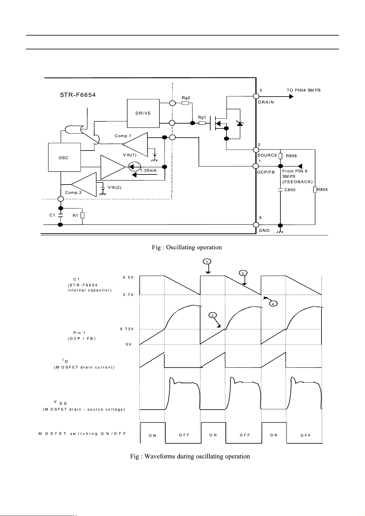
Service manual SC-150
-61-
5-9-2-2 STR-F6654 oscillating operation
Page 63

Service manual SC-150
-62-
When the MOSFET is ON, the STR-F6654 internal capacitor C1 is charged at the constant voltage 6.5V.
At the same time, the voltage at pin 1 (OCP / FB) increases with the same waveform as the MOSFET drain current.
When the pin 1 voltage reaches the threshold voltage V
TH1
= 0.73V, the STR-F6654 internal comparator 1 starts
operating. The STR-F6654 internal oscillator is inverted and the MOSFET turns OFF.
When the MOSFET turns OFF, charging of STR-F6654 internal capacitor C1 is released and C1 starts discharging
by the STR-F6654 internal resistance R1. So, C1 voltage starts falling in accordance with the gradient regulated by the
constant discharging time of C1 and R1. So, this means that the fixed time determined by C1 and R1 is the OFF-time
of the MOSFET.
When C1 voltage falls to around 3.7V, the STR-F6654 internal oscillator is reversed again and the MOSFET turns
ON. C1 is quickly charged to around 6.5V
The MOSFET continues to oscillate by repeating the above procedure.
5-9-2-3 STR-F6654 protection circuits
overcurrent protection function (OCP)
Overcurrent protection is performed pulse by pulse detecting at STR-F6654 pin 1 (OCP) the peak of the MOSFET
drain current in every pulse.
• latch circuit
This circuit sustains an output low from the STR-F6654 internal oscillator and stops operation of the power supply
when overvoltage protection (OVP) and thermal shutdown (TSD) circuit are under operation
thermal shutdown circuit (TSD)
This circuit triggers the latch circuit when the frame temperature of STR-F6654 IC exceeds 140
°
C
ov er voltage pr otection cir cuit (OVP)
This circuit triggers the latch circuit when the V
in
voltage exceeds 22V (typ.)
Page 64
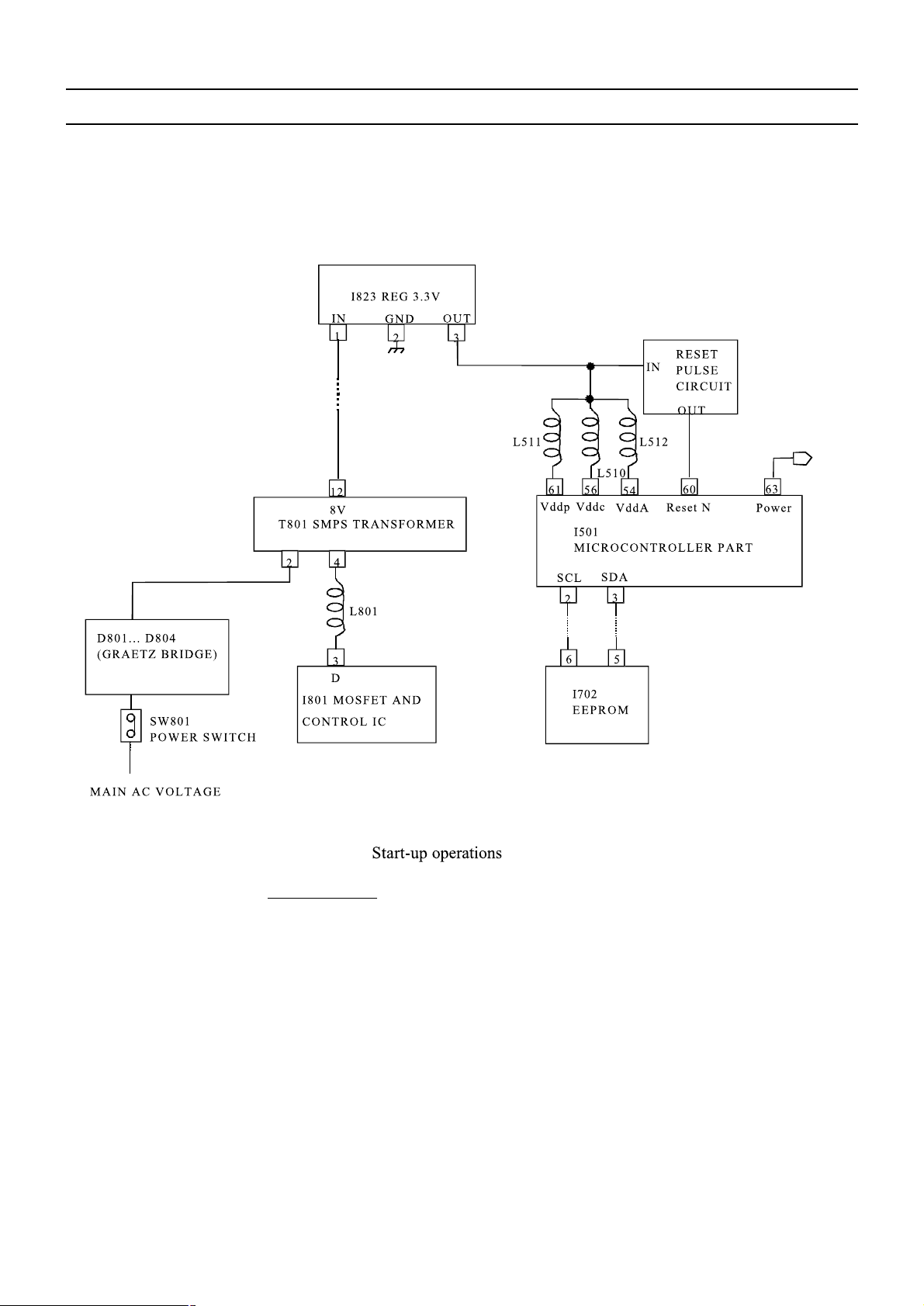
Service manual SC-150
-63-
5-10 TV start-up, TV normal run and stand by mode operations
5-10-1 TV start-up operations
*
Schematic diagram for start-up operations
*
TV start-up and microcontr
oller initialisation
- When SW801 power switch is pushed, main AC voltage is applied to T801 transformer (after rectification by D801...
D804 diodes). Then, T801 SMPS transformer starts operating and supplies DC volta ge to I823 (5V regulator).
- This regulator provides 5V / 3.3V DC voltage to I501 microcontroller power supply pins (pin 3 / pin 54) and to the
reset pulse circuit which provides reset pulse to I501 microcontroller reset pin (pin 58).
- Then, the microcontroller starts its initialisation. Its power pin (pin 1) is set to high which allows delivery of power
supply voltages (123V, 8V, 5V...). At this step, all IC’s start working but no picture appears on screen: I501 IC
doesn’t provide horizontal drive voltage.
- Then, the microcontroller consults I702 EEPROM via I2C bus to know the last TV set mode (normal run mode or
stand-by mode ) before switching off.
Page 65
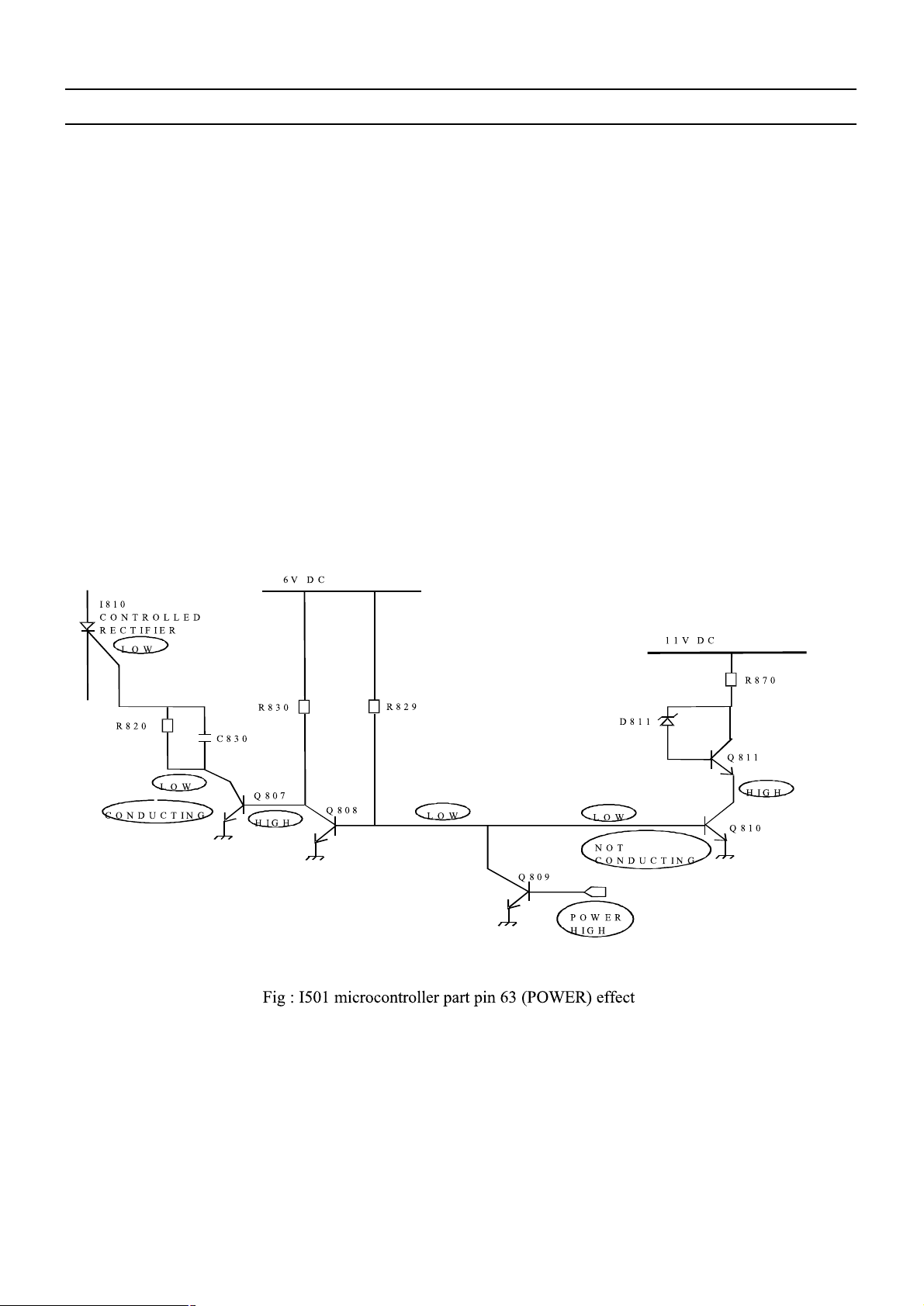
Service manual SC-150
-64-
. If the TV set was on normal run mode before switching off, the microcontroller delivers horizontal drive voltage at pin
24 and picture appears on screen.
. If the TV set was on stand-by mode before switching off, the microcontroller switches TV set to stand-by mode,
decreasing power pin voltage (pin 1).
5-10-2 TV normal run and stand-by mode operations
Depending on remote control commands, I501 microcontroller part pin 1 (power) is set to :
- high for normal run mode
- low for stand-by mode
a)
TV on normal run mode
*
I501 microcontroller part pin 1 (power) effect
I501 microcontroller part pin 1 (power) is connected to the following circuit :
Page 66
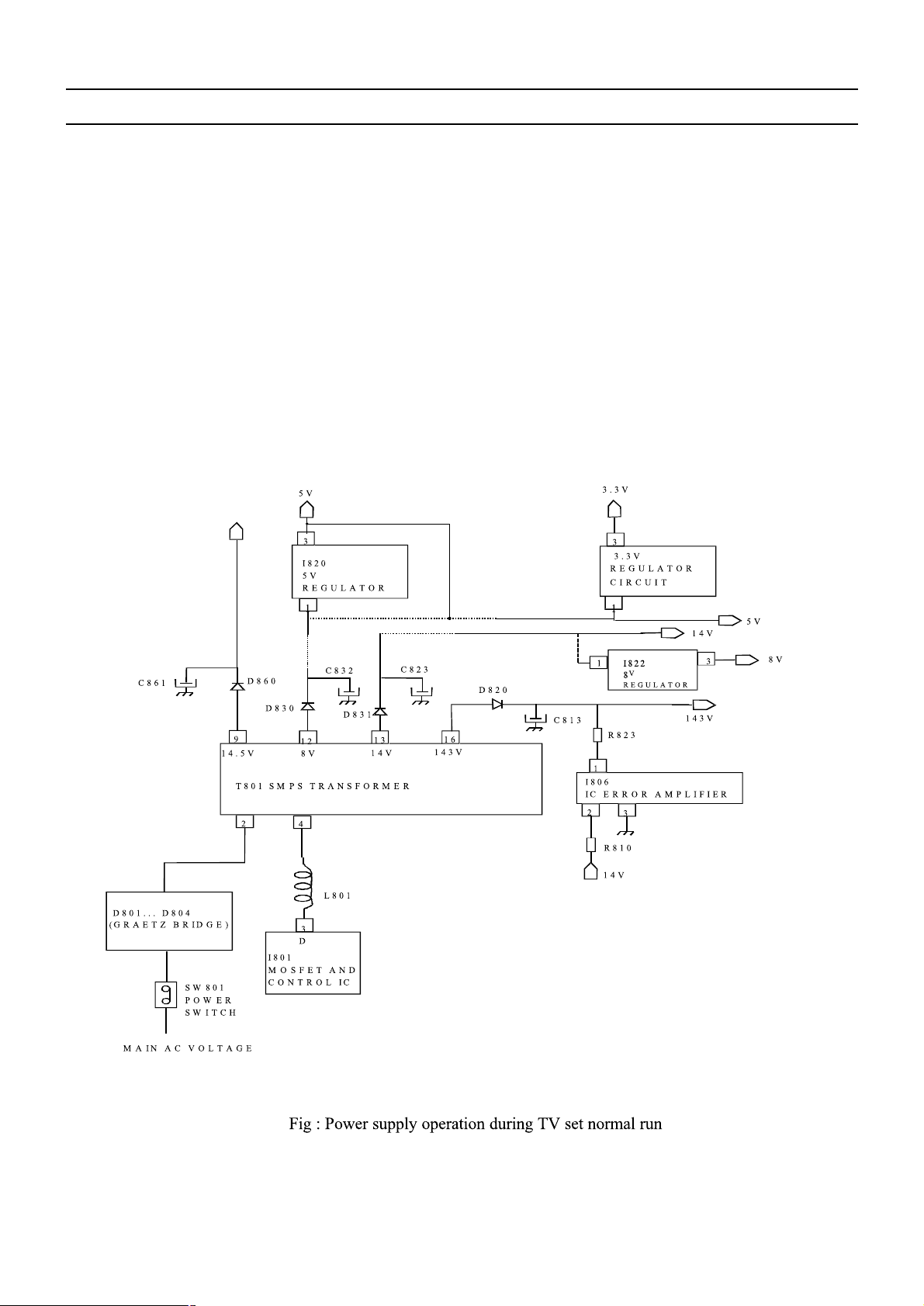
Service manual SC-150
-65-
On normal run mode, I501 microcontroller pin 1 (power) is set to high
S o, I810 controlled rectifier is not conducting
- Q809 is conducting. So, Q808 is not conducting and Q807 is conducting
- So, Q807 collector is connected to the ground and I810 controlled rectifier gate pin is set to low (no
conducting)
So, current from 14V DC voltage (from T801 SMPS transformer pin 13) does not flow through Q811 and Q810
transistors but flows through I806 IC error amplifier
- Q809 is conducting. So, Q810 is not conducting and no current flows from Q810 collector to the ground
Therefore, the power circuit diagram is the following one :
*
power supply circuit diagram during TV set normal run
Page 67
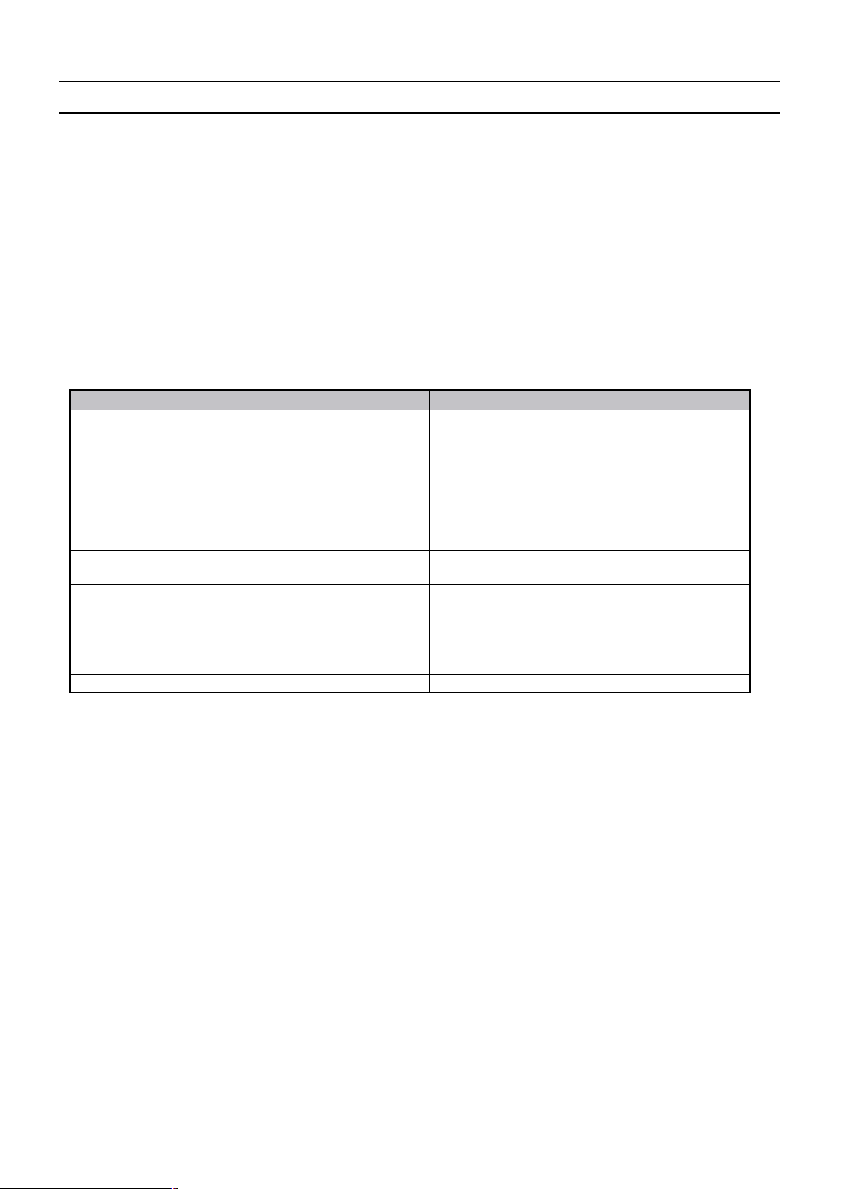
Service manual SC-150
-66-
*
power supply functioning during TV set normal run mode
- I801 transmits controlled pulses to T801 which generates DC voltages after rectifications by secondary part diodes
and electro capacitors (by example by D820 and C813 on 143V supply voltage line).
- 8V, 5V, 3.3V supply voltage lines have stabilized voltages obtained by I820, I822, I823 voltage regulators.
- On 143V supply voltage line, R823 resistor has been chosen to reach exact DC voltage required on this line.
- 143V supply voltage line includes an IC error amplifier (I806) which corrects unexpected DC voltage variations on
this line.
*
power supply IC delivery during TV set normal run
power supply line IC power supply delivery Remarks
143V FBT FBT supplies 43V to I301 vertical IC
FBT supplies 43
V to T401 H- drive for CP785
FBT supplies 12V to I301 vertical IC
FBT supplies 33V to the tuner
FBT supplies 188V to I901 video amplifier pin 6
14.5V I602 sound amplifier pins 3-16
14V T401 H- drive
8V I501 Main IC pins 14-39
I601 Sound Demod pins 38-39-40
5V I703 IR receiver pin 1
I501 Main IC pins 3-15-45
I601 Sound Demod pins 7-18-57
I702 EEPROM pin 8
tuner
3.3V I501 Main IC pins 25-54
b) TV set on stand-by mode
* TV set circuit diagram on stand-by mode
Page 68

Service manual SC-150
-67-
2
4
3
DRAIN
I801
MOFSET AND
CONTROL IC
1
MAIN AC VOLTAGE
I804
OPTO
COUPLER
I823 3.3V
REGULATOR
I703 IR
RECEIVER
FRONT
MASK
BUTTONS
I810
CONTROLLED
RECTIFIER
SWITCHING
CIRCUIT
T 801 SM PS TRA N S
I501
MAIN
IC
OCP
FB
D801...D804
GRAETZ BRIDGE
16
D821
I810
controlled rectifier
HIGH
C841
C840
R713
1
3
1
2
616456
54
7
63
CONDUCTING
IR IN
com
supply
voltage
KEY IN
POWER
R888
C888
Q809
Q810
Q811
D811
D825
R810
L801
D806
C808
SW801
POWER SWITCH
C850
R806
8
4
3
1
2
R870
HIGH
LOW
LOW
CONDUCTING
CONDUCTING
AROUND
6V dc
AROUND
3.3Vdc
Fig : Power supply operation in stand - by mode
Page 69
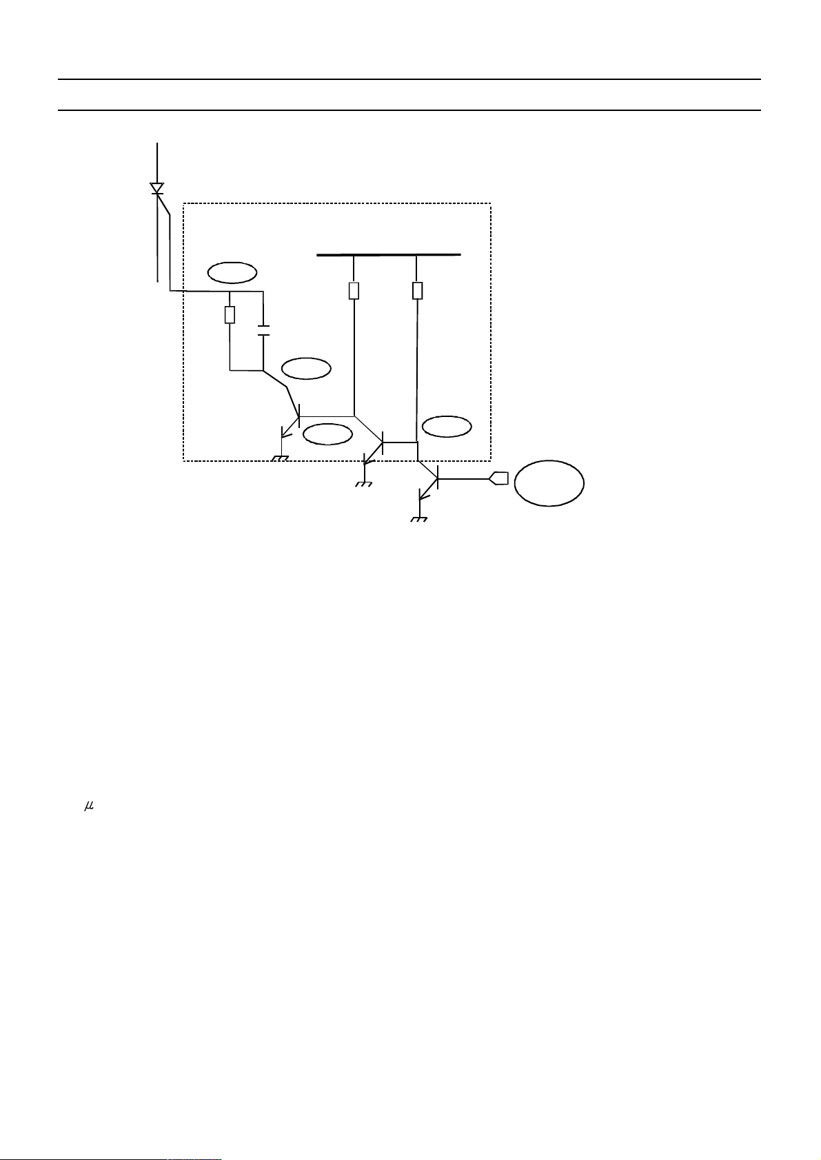
Service manual SC-150
-68-
I810
CONTROLLED
RECTIFIER
R820
R830
C830
R829
Q
808
6V DC
Q
809
Q
807
HIGH
HIGH
HIGH
LOW
POWER
LOW
Fig : I810 controlled rectifier switching circuit
* TV set stand-by mode operations
- On stand-by mode, I501 microcontroller pin 1 (power) is set to low.
- So, Q809 collector is set to high.
- Then, I810 controlled rectifier gate pin is set to high and I810 is conducting.
- So, current flows from pin 16 SMPS transformer to the ground via I804 optocoupler and Q810 and Q811 transistors
(which are conducting).
- In these conditions, I801 delivers pulses on light mode and T801 produces voltages with reduced power.
- As I810 is conducting, current flows also from pin 16 SMPS transformer to I823 (5V / 3.3V regulator) for I501
com, IR receiver and front mask buttons supply voltage (then, remote control or front mask buttons can be activated
to leave stand-by mode).
Page 70
Service manual SC-150
-69-
z_loc z_parts_code parts_name parts_descr
ZZ100 48B4846G22 TRANSMITTER REMOCON R-46G22 (AAA)
ZZ110 PEPKCPD037 PACKING AS DSC-3220E
M641 6520010100 STAPLE PIN AUTO W65
M681 4856812400 BAND PP AUTO T1.1XW17mmXL770M
M801 4958002200 BOX CARTON DW-4
M811 4958102500 PAD EPS
M821 4958200701 BAG P.E FOAM T0.5X1880X1380
ZZ120 PEBCSHD037 COVER BACK AS DSC-3220E
M211 4952102201 COVER BACK HIPS
M211E 4857817610 CLOTH BLACK FELT 300X20X0.7
ZZ131 58GD000004 COIL DEGAUSSING DC-3200(D)
ZZ132 49519A0110 CRT GROUND NET DSC-3210E
ZZ140 PECACAD037 CABINET AS DSC-3220E
M201A 4956000100 SCREW CRT FIX SWRM10A L=35
M201B 4856215401 WASHER RUBBER CR T1.0
M201C 7178301212 SCREW TAPPTITE TT2 WAS 3X12 MFZN BK
M201D 7178301212 SCREW TAPPTITE TT2 WAS 3X12 MFZN BK
M211A 7172401612 SCREW TAPPTITE TT2 TRS 4X16 MFZN BK
M211B 7172401612 SCREW TAPPTITE TT2 TRS 4X16 MFZN BK
M211C 7178301212 SCREW TAPPTITE TT2 WAS 3X12 MFZN BK
M211D 7172401612 SCREW TAPPTITE TT2 TRS 4X16 MFZN BK
M231 4952301301 PANEL CTRL HIPS PAINT
M353 4853535600 HOLDER CORD NYROLN 66
M481 4954801001 BUTTON POWER ABS PAINT
M481A 4856716000 SPRING SWPA PIE0.5
M541 4955400100 SPEC PLATE P.E FILM 91.5X63
M561 4855617400 MARK BRAND CU AU+ABS BK
M682 4856816300 CLAMP WIRE NYLON 6 (V0)
S601 4858315610 SPEAKER SP-5090F13
S601A 7178301212 SCREW TAPPTITE TT2 WAS 3X12 MFZN BK
S601R 4850703S52 CONNECTOR YH025-03+35098+ULW=400
S602 4858315610 SPEAKER SP-5090F13
S602A 7178301212 SCREW TAPPTITE TT2 WAS 3X12 MFZN BK
S602L 4850703S54 CONNECTOR YH025-03+35098+ULW=600
V901 4859639160 CRT W76ERF042X013
V901A 4850706N14 CONNECTOR YFSH500-06+YH396V+ULW=600
ZZ200 PEFMSJD037 MASK FRONT AS DSC-3220E
M201 4952002401 MASK FRONT HIPS PAINT
M201E 4857817610 CLOTH BLACK FELT 300X20X0.7
ZZ300 PEMPMSD037 PCB MAIN MANUAL AS DSC-3220E
10 2193102005 SOLDER BAR SN:PB=63:47 S63S-1320
30 2291050616 FLUX SOLDER JS-64T3
40 2291050301 FLUX SOLVENT IM-1000
C402 CMYH3C562J C MYLAR 1.6KV BUP 5600PF J
C403 CMYH3C752J C MYLAR 1.6KV BUP 7500PF J
C408 CMYE2G274J C MYLAR 400V PU 0.27MF J
C499 CEYD1H689W C ELECTRO 50V RHD 6.8MF (16X35.5)
C801 CL1UC3474M C LINE ACROSS 0.47MF 1J(UCVSNDF/SV)+Q/O
C805 CEYN2G181P C ELECTRO 400V LHS 180MF (25X35)
C812 CH1BFE472M C CERA AC AC400V 4700PF M U/C/V
C813 CEXF2E101V C ELECTRO 250V RSS 100MF 18X35.5
z_loc z_parts_code parts_name parts_descr
C890 CCYE3D103P C CERA 2KV E 0.01MF P
D403 DDGP30L—- DIODE DGP30L
D404 DRGP30J—- DIODE RGP30J
D820 DRGP30J—- DIODE RGP30J
D860 DRGP30J—- DIODE RGP30J
F801 5FSCB4022R FUSE CERA SEMKO F4AH 4A 250V MF51
I101 1TDA4470M- IC IF TDA4470-M
I301 1TDA8358J- IC VERTICAL TDA8358J
I301A 4857028227 HEAT SINK AL EX BK
I301B 7174301011 SCREW TAPPTITE TT2 RND 3X10 MFZN
I501 1DW3834AE2 IC MICOM DW3834-C4-AE2
I601 1MSP3410V3 IC SOUND PROCESSOR MSP3410G-PP-B8-V3
I602 1TDA8946J- IC AUDIO AMP TDA8946J
I602A 4857028227 HEAT SINK AL EX BK
I602B 7174301011 SCREW TAPPTITE TT2 RND 3X10 MFZN
I603 1KA4558—- IC AMP KA4558
I702 1CAT24C16P IC MEMORY CAT24WC16P
I801 1STRF6654- IC SMPS STR-F6654
I801A 4857027910 HEAT SINK AL EX
I801B 7174301211 SCREW TAPPTITE TT2 RND 3X12 MFZN
I804 1LTV817C— IC PHOTO COUPLER LTV-817C
I806 1SE130N—- IC SE130N
I810 TX0202DA— THYRISTOR X0202DA1BA2
I820 1KA7805—- IC REGULATOR KA7805
I820A 4857026901 HEAT SINK AL EX BK
I820B 7174300811 SCREW TAPPTITE TT2 RND 3X8 MFZN
I822 1KA7808—- IC REGULATOR KA7808
I822A 4857026901 HEAT SINK AL EX BK
I822B 7174300811 SCREW TAPPTITE TT2 RND 3X8 MFZN
I823 1KA7805—- IC REGULATOR KA7805
IA01 1MM1118—- IC A/V SWITCH MM1118
JPA1 4959103680 JACK SCART DSAM-0266
JPA2 4959103680 JACK SCART DSAM-0266
L150 58E0000041 COIL AFT TRF-A005
L380 5MC0000085 COIL CHOKE CH-100A
L381 5MC0000085 COIL CHOKE CH-100A
L401 58H0000077 COIL H-LINEARITY TRL-40A1
L402 58CD000022 COIL CHOKE CH-700A
L802 58C9430599 COIL CHOKE AZ-9004Y(94MH)
LF801 5PLF3020— FILTER LINE LF-3020
M351 4953500100 HOLDER CORD FR HIPS
M351A 7172401612 SCREW TAPPTITE TT2 TRS 4X16 MFZN BK
M381 4953802800 FRAME MAIN PCB FR HIPS BK
M381A 7178301212 SCREW TAPPTITE TT2 WAS 3X12 MFZN BK
M381B 7178301212 SCREW TAPPTITE TT2 WAS 3X12 MFZN BK
M681 4856815400 CLAMP WIRE NYLON 66
M683 4856812001 TIE CABLE NYLON66 DA100
P402 4859240120 CONN WAFER YFW500-06
P404 4859238620 CONN WAFER YPW500-02
P800 4859907410 CORD POWER AS M5206+TER=2250
M207 4853535500 HOLDER AC CORD NYLON 66
6-1. Service Parts List
Page 71
Service manual SC-150
-70-
z_loc z_parts_code parts_name parts_descr
M222 4859906111 CORD POWER M5206+H03VVH2-F=2250
M222T 4857417700 TERM CLAMP PT-01-T3
Q401 T2SD1880— TR 2SD1880
Q401A 4857024500 HEAT SINK AL EX B/K
Q401B 7174300811 SCREW TAPPTITE TT2 RND 3X8 MFZN
R801 DPC7R0M290 POSISTOR 2322 662 96709
R819 RX10T339J- R CEMENT 10W 3.3 OHM J TRIPOD
RB02 RV4121103P R SEMI FIXED NVZ6THT 10K OHM
SF01 5PK3953M— FILTER SAW K3953M
SF02 5PK9650M— FILTER SAW K9650M
T401 50D19A1—- TRANS DRIVE TD-19A1
T402 5DH0000028 FBT LTC-305
T801 50M4936B2- TRANS SMPS 2094.0057
T803 58CD000023 COIL CHOKE HYBRID HCA208-049A
U100 4859721530 TUNER VARACTOR DT5-BF18D N
X501 5XE20R250E CRYSTAL QUARTZ HC-49/U 20.2500MHZ 30PPM
X601 5XE18R432E CRYSTAL QUARTZ HC-49/U 18.43200MHZ 30PPM
Z101 5PMKT40MA- FILTER CERA MKT40MA100P
Z153 5PYXT5R5MB FILTER CERA XT 5.5MB
ZZ200 PEMPJ0D037 PCB MAIN (RHU) AS DSC-3220E
C315 CEXF2C470C C ELECTRO 160V RUS 47MF (13X25) TP
C415 CEXF2E479V C ELECTRO 250V RSS 4.7MF (10X16)TP
C430 CCXB3D681K C CERA 2KV B 680PF K (TAPPING)
C440 CMXE2G273J C MYLAR 400V PU 0.027MF J (TP)
C502 CEXF1C102V C ELECTRO 16V RSS 1000MF (10X20) TP
C553 CEXF1C102V C ELECTRO 16V RSS 1000MF (10X20) TP
C604 CEXF1E102V C ELECTRO 25V RSS 1000MF (13X20) TP
C811 CCXB3D681K C CERA 2KV B 680PF K (TAPPING)
C814 CEXF2E470V C ELECTRO 250V RSS 47MF (16X25) TP
C823 CEXF1E102V C ELECTRO 25V RSS 1000MF (13X20) TP
C832 CEXF1E102V C ELECTRO 25V RSS 1000MF (13X20) TP
C840 CEXF1C222V C ELECTRO 16V RSS 2200MF (16X31.5) TP
C841 CEXF1C332V C ELECTRO 16V RSS 3300MF (16X25) TP
C861 CEXF1E102C C ELECTRO 25V RUS 1000MF (13X20) TP
ZZ200 PEMPJBD037 PCB MAIN M-10 AS DSC-3220E
E001 4856310600 EYE LET BSR T0.2 (R2.3)
E002 4856310600 EYE LET BSR T0.2 (R2.3)
E003 4856310600 EYE LET BSR T0.2 (R2.3)
E004 4856310600 EYE LET BSR T0.2 (R2.3)
E005 4856310300 EYE LET BSR T0.2 (R1.6)
E006 4856310300 EYE LET BSR T0.2 (R1.6)
E007 4856310300 EYE LET BSR T0.2 (R1.6)
E008 4856310300 EYE LET BSR T0.2 (R1.6)
E009 4856310600 EYE LET BSR T0.2 (R2.3)
E010 4856310600 EYE LET BSR T0.2 (R2.3)
E011 4856310300 EYE LET BSR T0.2 (R1.6)
E012 4856310600 EYE LET BSR T0.2 (R2.3)
E013 4856310600 EYE LET BSR T0.2 (R2.3)
E014 4856310600 EYE LET BSR T0.2 (R2.3)
E015 4856310600 EYE LET BSR T0.2 (R2.3)
E016 4856310600 EYE LET BSR T0.2 (R2.3)
E017 4856310600 EYE LET BSR T0.2 (R2.3)
z_loc z_parts_code parts_name parts_descr
E018 4856310300 EYE LET BSR T0.2 (R1.6)
E019 4856310300 EYE LET BSR T0.2 (R1.6)
E020 4856310300 EYE LET BSR T0.2 (R1.6)
E021 4856310600 EYE LET BSR T0.2 (R2.3)
E022 4856310600 EYE LET BSR T0.2 (R2.3)
E023 4856310300 EYE LET BSR T0.2 (R1.6)
E024 4856310300 EYE LET BSR T0.2 (R1.6)
E025 4856310600 EYE LET BSR T0.2 (R2.3)
E026 4856310600 EYE LET BSR T0.2 (R2.3)
E027 4856310600 EYE LET BSR T0.2 (R2.3)
E028 4856310600 EYE LET BSR T0.2 (R2.3)
E029 4856310600 EYE LET BSR T0.2 (R2.3)
E030 4856310600 EYE LET BSR T0.2 (R2.3)
E031 4856310300 EYE LET BSR T0.2 (R1.6)
E032 4856310600 EYE LET BSR T0.2 (R2.3)
E033 4856310300 EYE LET BSR T0.2 (R1.6)
E034 4856310300 EYE LET BSR T0.2 (R1.6)
E035 4856310300 EYE LET BSR T0.2 (R1.6)
E037 4856310600 EYE LET BSR T0.2 (R2.3)
E038 4856310600 EYE LET BSR T0.2 (R2.3)
E039 4856310600 EYE LET BSR T0.2 (R2.3)
E040 4856310600 EYE LET BSR T0.2 (R2.3)
E041 4856310300 EYE LET BSR T0.2 (R1.6)
E042 4856310300 EYE LET BSR T0.2 (R1.6)
E043 4856310300 EYE LET BSR T0.2 (R1.6)
E044 4856310300 EYE LET BSR T0.2 (R1.6)
E045 4856310300 EYE LET BSR T0.2 (R1.6)
E046 4856310300 EYE LET BSR T0.2 (R1.6)
E047 4856310300 EYE LET BSR T0.2 (R1.6)
E048 4856310300 EYE LET BSR T0.2 (R1.6)
E049 4856310300 EYE LET BSR T0.2 (R1.6)
P102 485923162S CONN WAFER YW025-03 (STICK)
P401 485923172S CONN WAFER YW025-04 (STICK)
P403 485923202S CONN WAFER YW025-07 (STICK)
P501 485923182S CONN WAFER YW025-05 (STICK)
P502 485923162S CONN WAFER YW025-03 (STICK)
P603 485923172S CONN WAFER YW025-04 (STICK)
P701 485923512S CONN WAFER YW025-08 (STICK)
P801A 4857417500 TERM PIN DA-IB0214(D2.3/DY PIN)
P801B 4857417500 TERM PIN DA-IB0214(D2.3/DY PIN)
P802A 4857417500 TERM PIN DA-IB0214(D2.3/DY PIN)
P802B 4857417500 TERM PIN DA-IB0214(D2.3/DY PIN)
P803A 4857417500 TERM PIN DA-IB0214(D2.3/DY PIN)
P803B 4857417500 TERM PIN DA-IB0214(D2.3/DY PIN)
PA01 485923522S CONN WAFER YW025-09 (STICK)
R399 RS02Z180JS R M-OXIDE FILM 2W 18 OHM J SMALL
R406 RS02Z681JS R M-OXIDE FILM 2W 680 OHM J SMALL
R415 RS02Z102JS R M-OXIDE FILM 2W 1K OHM J SMALL
R450 RS02Z223JS R M-OXIDE FILM 2W 22K OHM J SMALL
R802 RS02Z753JS R M-OXIDE FILM 2W 75K OHM J SMALL
R803 RS02Z473JS R M-OXIDE FILM 2W 47K OHM J SMALL
R804 RS02Z158J- R M-OXIDE FILM 2W 0.15 OHM J
Page 72

Service manual SC-150
-71-
z_loc z_parts_code parts_name parts_descr
R850 RS02Z129JS R M-OXIDE FILM 2W 1.2 OHM J SMALL
R890 RS02Z683J- R M-OXIDE FILM 2W 68K OHM J (TAPPING)
SP01 485923162S CONN WAFER YW025-03 (STICK)
SP02 485923162S CONN WAFER YW025-03 (STICK)
ZZ200 PEMPJRD037 PCB MAIN RADIAL AS DSC-3220E
C102 CEXF1H470V C ELECTRO 50V RSS 47MF (6.3X11) TP
C106 CEXF1C221V C ELECTRO 16V RSS 220MF (8X11.5) TP
C110 CXCH1H150J C CERA 50V CH 15PF J (TAPPING)
C117 CEXF1H229V C ELECTRO 50V RSS 2.2MF (5X11) TP
C118 CMXL1J474J C MYLAR 63V MEU 0.47MF J
C121 CEXF1H100V C ELECTRO 50V RSS 10MF (5X11) TP
C152 CEXF1H100V C ELECTRO 50V RSS 10MF (5X11) TP
C153 CEXF1H229V C ELECTRO 50V RSS 2.2MF (5X11) TP
C156 CBXF1H104Z C CERA SEMI 50V F 0.1MF Z (TAPPING)
C157 CEXF1H100V C ELECTRO 50V RSS 10MF (5X11) TP
C158 CBXF1H104Z C CERA SEMI 50V F 0.1MF Z (TAPPING)
C164 CEXF1E470V C ELECTRO 25V RSS 47MF (5X11) TP
C301 CMXL1J224J C MYLAR 63V MEU 0.22MF J (TP)
C305 CEXF1E221V C ELECTRO 25V RSS 220MF (8X11.5) TP
C313 CMXL1J104J C MYLAR 63V MEU 0.1MF J
C320 CBXF1H104Z C CERA SEMI 50V F 0.1MF Z (TAPPING)
C340 CMXL1J683J C MYLAR 63V MEU 0.068MF J
C350 CMXL1J103J C MYLAR 63V MEU 0.01MF J
C351 CMXL1J103J C MYLAR 63V MEU 0.01MF J
C401 CEXF1H101V C ELECTRO 50V RSS 100MF (8X11.5) TP
C412 CEXF2C339V C ELECTRO 160V RSS 3.3MF (8X16) TP
C418 CCXB1H102K C CERA 50V B 1000PF K (TAPPING)
C420 CCXB2H222K C CERA 500V B 2200PF K (TAPPING)
C424 CMXM2A333J C MYLAR 100V 0.033MF J (TP)
C431 CMXM2A103J C MYLAR 100V 0.01MF J (TP)
C504 CEXF1H470V C ELECTRO 50V RSS 47MF (6.3X11) TP
C508 CEXF1H220V C ELECTRO 50V RSS 22MF (5X11) TP
C511 CEXF1H100V C ELECTRO 50V RSS 10MF (5X11) TP
C519 CEXF1H109V C ELECTRO 50V RSS 1MF (5X11) TP
C520 CEXF1H109V C ELECTRO 50V RSS 1MF (5X11) TP
C521 CEXF1H109V C ELECTRO 50V RSS 1MF (5X11) TP
C522 CEXF1H109V C ELECTRO 50V RSS 1MF (5X11) TP
C525 CEXF1H220V C ELECTRO 50V RSS 22MF (5X11) TP
C546 CEXF1H339V C ELECTRO 50V RSS 3.3MF (5X11) TP
C549 CEXF1H229V C ELECTRO 50V RSS 2.2MF (5X11) TP
C597 CEXF1H220V C ELECTRO 50V RSS 22MF (5X11) TP
C602 CEXF1E221V C ELECTRO 25V RSS 220MF (8X11.5) TP
C605 CEXF1E470V C ELECTRO 25V RSS 47MF (5X11) TP
C608 CEXF1H100V C ELECTRO 50V RSS 10MF (5X11) TP
C610 CEXF1H100V C ELECTRO 50V RSS 10MF (5X11) TP
C611 CEXF1H339V C ELECTRO 50V RSS 3.3MF (5X11) TP
C612 CEXF1H109V C ELECTRO 50V RSS 1MF (5X11) TP
C613 CEXF1H109V C ELECTRO 50V RSS 1MF (5X11) TP
C614 CEXF1H109V C ELECTRO 50V RSS 1MF (5X11) TP
C615 CEXF1H109V C ELECTRO 50V RSS 1MF (5X11) TP
C616 CEXF1H100V C ELECTRO 50V RSS 10MF (5X11) TP
C619 CEXF1E221V C ELECTRO 25V RSS 220MF (8X11.5) TP
z_loc z_parts_code parts_name parts_descr
C623 CEXF1H109V C ELECTRO 50V RSS 1MF (5X11) TP
C624 CEXF1H109V C ELECTRO 50V RSS 1MF (5X11) TP
C625 CEXF1E101V C ELECTRO 25V RSS 100MF (6.3X11) TP
C626 CEXF1E101V C ELECTRO 25V RSS 100MF (6.3X11) TP
C627 CEXF1E470V C ELECTRO 25V RSS 47MF (5X11) TP
C628 CEXF1E470V C ELECTRO 25V RSS 47MF (5X11) TP
C630 CEXF1E470V C ELECTRO 25V RSS 47MF (5X11) TP
C632 CEXF1E479A C ELECTRO 25V RSM 4.7MF
C633 CEXF1E479A C ELECTRO 25V RSM 4.7MF
C634 CEXF1H100V C ELECTRO 50V RSS 10MF (5X11) TP
C636 CEXF1H470V C ELECTRO 50V RSS 47MF (6.3X11) TP
C638 CEXF1H479V C ELECTRO 50V RSS 4.7MF (5X11) TP
C639 CEXF1H479V C ELECTRO 50V RSS 4.7MF (5X11) TP
C641 CEXF1E101V C ELECTRO 25V RSS 100MF (6.3X11) TP
C642 CEXF1E101V C ELECTRO 25V RSS 100MF (6.3X11) TP
C660 CEXF1C100A C ELECTRO 16V RSM 10MF 5X7
C661 CMXL1J224J C MYLAR 63V MEU 0.22MF J (TP)
C662 CMXL1J224J C MYLAR 63V MEU 0.22MF J (TP)
C665 CCXB1H222K C CERA 50V B 2200PF K (TAPPING)
C666 CBXF1H104Z C CERA SEMI 50V F 0.1MF Z (TAPPING)
C667 CCXB1H222K C CERA 50V B 2200PF K (TAPPING)
C668 CMXL1J224J C MYLAR 63V MEU 0.22MF J (TP)
C669 CMXL1J224J C MYLAR 63V MEU 0.22MF J (TP)
C670 CEXF1H100V C ELECTRO 50V RSS 10MF (5X11) TP
C770 CEXF1C101V C ELECTRO 16V RSS 100MF (6.3X11) TP
C803 CCXF3A472Z C CERA 1KV F 4700PF Z (T)
C804 CCXF3A472Z C CERA 1KV F 4700PF Z (T)
C806 CEXF1H330V C ELECTRO 50V RSS 33MF (6.3X11) TP
C807 CCXF1H473Z C CERA 50V F 0.047MF Z (TAPPING)
C808 CEXF1H100V C ELECTRO 50V RSS 10MF (5X11) TP
C809 CCXB1H102K C CERA 50V B 1000PF K (TAPPING)
C820 CCXB3A471K C CERA 1KV B 470PF K (T)
C821 CCXB2H102K C CERA 500V B 1000PF K (TAPPING)
C824 CCXB3A471K C CERA 1KV B 470PF K (T)
C825 CCXB2H101K C CERA 500V B 100PF K (TAPPING)
C831 CCXB3A471K C CERA 1KV B 470PF K (T)
C835 CEXF1H470V C ELECTRO 50V RSS 47MF (6.3X11) TP
C844 CEXF1E101V C ELECTRO 25V RSS 100MF (6.3X11) TP
C850 CCXB1H821K C CERA 50V B 820PF K (TAPPING)
C863 CEXF1E101V C ELECTRO 25V RSS 100MF (6.3X11) TP
C866 CCXB3A471K C CERA 1KV B 470PF K (T)
CA12 CEXF1H100V C ELECTRO 50V RSS 10MF (5X11) TP
CA33 CEXF1H100V C ELECTRO 50V RSS 10MF (5X11) TP
F801A 4857415001 CLIP FUSE PFC5000-0702
F801B 4857415001 CLIP FUSE PFC5000-0702
I805 1K1A7042AP IC REGULATOR KIA7042AP
Q103 TKTC3198Y- TR KTC3198Y
Q104 TKTC3198Y- TR KTC3198Y
Q120 TKTC3198Y- TR KTC3198Y
Q150 TKTC3198Y- TR KTC3198Y
Q151 TKTC3198Y- TR KTC3198Y
Q333 TKTC3198Y- TR KTC3198Y
Page 73
Service manual SC-150
-72-
z_loc z_parts_code parts_name parts_descr
Q334 TKTC3198Y- TR KTC3198Y
Q402 T2SD1207T- TR 2SD1207-T (TAPPING)
Q510 TKTC3198Y- TR KTC3198Y
Q511 TKTC3198Y- TR KTC3198Y
Q542 TKTA1266Y- TR KTA1266Y (TP)
Q543 TKTA1266Y- TR KTA1266Y (TP)
Q544 TKTA1266Y- TR KTA1266Y (TP)
Q550 TKTC3198Y- TR KTC3198Y
Q599 TKTA1266Y- TR KTA1266Y (TP)
Q601 TKTA1266Y- TR KTA1266Y (TP)
Q702 TKTA1266Y- TR KTA1266Y (TP)
Q703 TKTC3198Y- TR KTC3198Y
Q807 TKTC3198Y- TR KTC3198Y
Q808 TKTC3198Y- TR KTC3198Y
Q809 TKTC3198Y- TR KTC3198Y
Q810 TKTC3198Y- TR KTC3198Y
Q811 TKTC3198Y- TR KTC3198Y
Q850 TKTC3198Y- TR KTC3198Y
Q851 TKTC3198Y- TR KTC3198Y
QA01 TKTC3198Y- TR KTC3198Y
RB10 RV5426103P R SEMI FIXED ENV-DJAA03B14 10K OHM B
Z603 5PXF1B471M FILTER EMI CFI 06 B 1H 470PF
Z604 5PXF1B471M FILTER EMI CFI 06 B 1H 470PF
Z605 5PXF1B471M FILTER EMI CFI 06 B 1H 470PF
Z606 5PXF1B471M FILTER EMI CFI 06 B 1H 470PF
Z607 5PXF1B471M FILTER EMI CFI 06 B 1H 470PF
Z608 5PXF1B471M FILTER EMI CFI 06 B 1H 470PF
ZZ200 PEMPJAD037 PCB MAIN AXIAL AS DSC-3220E
A001 4959812224 PCB MAIN 330X246 D1B
C101 CCZB1H101K C CERA 50V B 100PF K (AXIAL)
C103 CCZB1H102K C CERA 50V B 1000PF K (AXIAL)
C104 CCZB1H102K C CERA 50V B 1000PF K (AXIAL)
C116 CBZF1H104Z C CERA SEMI 50V F 0.1MF Z
C119 CCZF1H103Z C CERA 50V F 0.01MF Z
C120 CCZB1H102K C CERA 50V B 1000PF K (AXIAL)
C151 CCZF1H103Z C CERA 50V F 0.01MF Z
C154 CCZF1H103Z C CERA 50V F 0.01MF Z
C160 CCZF1H103Z C CERA 50V F 0.01MF Z
C161 CZCH1H220J C CERA 50V CH 22PF J (AXIAL)
C163 CCZF1H103Z C CERA 50V F 0.01MF Z
C341 CCZB1H102K C CERA 50V B 1000PF K (AXIAL)
C370 CCZF1H473Z C CERA 50V F 0.047MF Z
C500 CCZF1H103Z C CERA 50V F 0.01MF Z
C501 CCZF1H103Z C CERA 50V F 0.01MF Z
C503 CBZF1H104Z C CERA SEMI 50V F 0.1MF Z
C506 CBZF1H104Z C CERA SEMI 50V F 0.1MF Z
C507 CCZF1H103Z C CERA 50V F 0.01MF Z
C509 CCZF1H103Z C CERA 50V F 0.01MF Z
C510 CCZF1H473Z C CERA 50V F 0.047MF Z
C512 CCZF1H103Z C CERA 50V F 0.01MF Z
C513 CCZB1H471K C CERA 50V B 470PF K (AXIAL)
C516 CCZB1H102K C CERA 50V B 1000PF K (AXIAL)
z_loc z_parts_code parts_name parts_descr
C526 CBZF1H104Z C CERA SEMI 50V F 0.1MF Z
C528 CCZF1H223Z C CERA 50V F 0.022MF Z
C529 CCZF1H223Z C CERA 50V F 0.022MF Z
C530 CCZF1H223Z C CERA 50V F 0.022MF Z
C534 CCZB1H333K C CERA 50V B 0.033MF K AXL
C535 CCZB1H333K C CERA 50V B 0.033MF K AXL
C536 CCZB1H333K C CERA 50V B 0.033MF K AXL
C547 CBZF1H104Z C CERA SEMI 50V F 0.1MF Z
C548 CBZF1H104Z C CERA SEMI 50V F 0.1MF Z
C554 CBZF1H104Z C CERA SEMI 50V F 0.1MF Z
C560 CCZB1H101K C CERA 50V B 100PF K (AXIAL)
C561 CCZB1H101K C CERA 50V B 100PF K (AXIAL)
C568 CBZF1H104Z C CERA SEMI 50V F 0.1MF Z
C571 CCZB1H101K C CERA 50V B 100PF K (AXIAL)
C578 CCZB1H221K C CERA 50V B 220PF K (AXIAL)
C579 CCZB1H221K C CERA 50V B 220PF K (AXIAL)
C581 CCZB1H101K C CERA 50V B 100PF K (AXIAL)
C585 CCZB1H101K C CERA 50V B 100PF K (AXIAL)
C587 CCZB1H102K C CERA 50V B 1000PF K (AXIAL)
C589 CCZB1H221K C CERA 50V B 220PF K (AXIAL)
C590 CZCH1H309C C CERA 50V CH 3PF C (AXIAL)
C591 CZCH1H309C C CERA 50V CH 3PF C (AXIAL)
C601 CCZB1H102K C CERA 50V B 1000PF K (AXIAL)
C603 CCZB1H102K C CERA 50V B 1000PF K (AXIAL)
C606 CCZB1H222K C CERA 50V B 2200PF K AXIAL
C607 CCZB1H102K C CERA 50V B 1000PF K (AXIAL)
C617 CBZF1H104Z C CERA SEMI 50V F 0.1MF Z
C618 CCZB1H102K C CERA 50V B 1000PF K (AXIAL)
C620 CZCH1H309C C CERA 50V CH 3PF C (AXIAL)
C621 CZCH1H309C C CERA 50V CH 3PF C (AXIAL)
C622 CZCH1H680J C CERA CH 50V 68PF J AXL 52MM
C629 CBZF1H104Z C CERA SEMI 50V F 0.1MF Z
C631 CBZF1H104Z C CERA SEMI 50V F 0.1MF Z
C635 CCZB1H102K C CERA 50V B 1000PF K (AXIAL)
C637 CCZB1H222K C CERA 50V B 2200PF K AXIAL
C650 CZCH1H680J C CERA CH 50V 68PF J AXL 52MM
C690 CBZF1H104Z C CERA SEMI 50V F 0.1MF Z
C691 CBZF1H104Z C CERA SEMI 50V F 0.1MF Z
C702 CBZF1H104Z C CERA SEMI 50V F 0.1MF Z
C830 CBZF1H104Z C CERA SEMI 50V F 0.1MF Z
C888 CCZF1H103Z C CERA 50V F 0.01MF Z
CA01 CCZB1H101K C CERA 50V B 100PF K (AXIAL)
CA02 CCZB1H101K C CERA 50V B 100PF K (AXIAL)
CA03 CCZB1H101K C CERA 50V B 100PF K (AXIAL)
CA04 CCZB1H102K C CERA 50V B 1000PF K (AXIAL)
CA07 CCZB1H102K C CERA 50V B 1000PF K (AXIAL)
CA10 CCZB1H102K C CERA 50V B 1000PF K (AXIAL)
CA13 CCZB1H471K C CERA 50V B 470PF K (AXIAL)
CA14 CCZB1H471K C CERA 50V B 470PF K (AXIAL)
CA15 CCZB1H102K C CERA 50V B 1000PF K (AXIAL)
CA16 CCZB1H102K C CERA 50V B 1000PF K (AXIAL)
CA17 CCZB1H102K C CERA 50V B 1000PF K (AXIAL)
Page 74
Service manual SC-150
-73-
z_loc z_parts_code parts_name parts_descr
CA18 CCZB1H102K C CERA 50V B 1000PF K (AXIAL)
CA30 CCZF1H103Z C CERA 50V F 0.01MF Z
CA31 CCZF1H103Z C CERA 50V F 0.01MF Z
CA34 CCZB1H102K C CERA 50V B 1000PF K (AXIAL)
CA35 CCZB1H102K C CERA 50V B 1000PF K (AXIAL)
CA37 CCZB1H561K C CERA 50V B 560PF K
CA38 CCZB1H561K C CERA 50V B 560PF K
D100 DUZ33B—— DIODE ZENER UZ-33B
D101 D1N4148—- DIODE 1N4148 (TAPPING)
D103 DBA282—— DIODE BA282
D313 DRGP15J—- DIODE RGP15J
D351 DUZ12BM—- DIODE ZENER UZ-12BM (UNIZON)
D360 DUZ22BM—- DIODE ZENER UZ-22BM
D361 DUZ33B—— DIODE ZENER UZ-33B
D362 DUZ33B—— DIODE ZENER UZ-33B
D367 DUZ33B—— DIODE ZENER UZ-33B
D405 DRGP15J—- DIODE RGP15J
D407 DRGP15J—- DIODE RGP15J
D408 DRGP15J—- DIODE RGP15J
D410 D1N4004S— DIODE 1N4004S
D411 D1N4004S— DIODE 1N4004S
D450 DRGP15J—- DIODE RGP15J
D520 D1N4148—- DIODE 1N4148 (TAPPING)
D521 D1N4148—- DIODE 1N4148 (TAPPING)
D533 D1N4148—- DIODE 1N4148 (TAPPING)
D534 D1N4148—- DIODE 1N4148 (TAPPING)
D537 D1N4148—- DIODE 1N4148 (TAPPING)
D550 D1N4148—- DIODE 1N4148 (TAPPING)
D551 D1N4148—- DIODE 1N4148 (TAPPING)
D591 DUZ2R7B—- DIODE ZENER UZ-2.7B
D597 D1N4148—- DIODE 1N4148 (TAPPING)
D598 D1N4148—- DIODE 1N4148 (TAPPING)
D599 DUZ5R6BM— DIODE ZENER UZ-5.6BM
D601 D1N4148—- DIODE 1N4148 (TAPPING)
D602 D1N4148—- DIODE 1N4148 (TAPPING)
D603 D1N4148—- DIODE 1N4148 (TAPPING)
D604 D1N4148—- DIODE 1N4148 (TAPPING)
D700 DUZ5R6BM— DIODE ZENER UZ-5.6BM
D801 DLT2A05G— DIODE LT2A05G (TP)
D802 DLT2A05G— DIODE LT2A05G (TP)
D803 DLT2A05G— DIODE LT2A05G (TP)
D804 DLT2A05G— DIODE LT2A05G (TP)
D805 DRGP15J—- DIODE RGP15J
D806 DRGP15J—- DIODE RGP15J
D808 DRGP15J—- DIODE RGP15J
D809 DRGP15J—- DIODE RGP15J
D811 DUZ6R2BM— DIODE ZENER UZ-6.2BM
D821 DRGP15J—- DIODE RGP15J
D824 D1N4148—- DIODE 1N4148 (TAPPING)
D825 D1N4148—- DIODE 1N4148 (TAPPING)
D830 DRGP15J—- DIODE RGP15J
D831 DRGP15J—- DIODE RGP15J
z_loc z_parts_code parts_name parts_descr
D840 D1N4148—- DIODE 1N4148 (TAPPING)
D841 D1N4148—- DIODE 1N4148 (TAPPING)
D850 DUZ2R7B—- DIODE ZENER UZ-2.7B
D890 DRU1P——- DIODE RU1P
DA03 DUZ5R1BM— DIODE ZENER UZ-5.1BM
DA06 DUZ5R6BM— DIODE ZENER UZ-5.6BM
DA07 DUZ5R1BM— DIODE ZENER UZ-5.1BM
DA08 DUZ5R6BM— DIODE ZENER UZ-5.6BM
DA09 DUZ5R6BM— DIODE ZENER UZ-5.6BM
DA1 DUZ5R1BM— DIODE ZENER UZ-5.1BM
DA10 DUZ5R6BM— DIODE ZENER UZ-5.6BM
DA11 DUZ5R6BM— DIODE ZENER UZ-5.6BM
DA15 DUZ5R6BM— DIODE ZENER UZ-5.6BM
DA16 DUZ5R6BM— DIODE ZENER UZ-5.6BM
DA20 DUZ5R6BM— DIODE ZENER UZ-5.6BM
DA27 DUZ5R6BM— DIODE ZENER UZ-5.6BM
DA32 DUZ5R6BM— DIODE ZENER UZ-5.6BM
J101 85801065GY WIRE COPPER AWG22 1/0.65 TIN COATING
J103 85801065GY WIRE COPPER AWG22 1/0.65 TIN COATING
J104 85801065GY WIRE COPPER AWG22 1/0.65 TIN COATING
J105 85801065GY WIRE COPPER AWG22 1/0.65 TIN COATING
J106 85801065GY WIRE COPPER AWG22 1/0.65 TIN COATING
J107 85801065GY WIRE COPPER AWG22 1/0.65 TIN COATING
J108 85801065GY WIRE COPPER AWG22 1/0.65 TIN COATING
J109 85801065GY WIRE COPPER AWG22 1/0.65 TIN COATING
J110 85801065GY WIRE COPPER AWG22 1/0.65 TIN COATING
J111 85801065GY WIRE COPPER AWG22 1/0.65 TIN COATING
J112 85801065GY WIRE COPPER AWG22 1/0.65 TIN COATING
J113 85801065GY WIRE COPPER AWG22 1/0.65 TIN COATING
J114 85801065GY WIRE COPPER AWG22 1/0.65 TIN COATING
J115 85801065GY WIRE COPPER AWG22 1/0.65 TIN COATING
J116 85801065GY WIRE COPPER AWG22 1/0.65 TIN COATING
J117 85801065GY WIRE COPPER AWG22 1/0.65 TIN COATING
J118 85801065GY WIRE COPPER AWG22 1/0.65 TIN COATING
J119 85801065GY WIRE COPPER AWG22 1/0.65 TIN COATING
J120 85801065GY WIRE COPPER AWG22 1/0.65 TIN COATING
J121 85801065GY WIRE COPPER AWG22 1/0.65 TIN COATING
J122 85801065GY WIRE COPPER AWG22 1/0.65 TIN COATING
J123 85801065GY WIRE COPPER AWG22 1/0.65 TIN COATING
J124 85801065GY WIRE COPPER AWG22 1/0.65 TIN COATING
J125 85801065GY WIRE COPPER AWG22 1/0.65 TIN COATING
J126 85801065GY WIRE COPPER AWG22 1/0.65 TIN COATING
J127 85801065GY WIRE COPPER AWG22 1/0.65 TIN COATING
J128 85801065GY WIRE COPPER AWG22 1/0.65 TIN COATING
J129 85801065GY WIRE COPPER AWG22 1/0.65 TIN COATING
J130 85801065GY WIRE COPPER AWG22 1/0.65 TIN COATING
J131 85801065GY WIRE COPPER AWG22 1/0.65 TIN COATING
J132 85801065GY WIRE COPPER AWG22 1/0.65 TIN COATING
J133 85801065GY WIRE COPPER AWG22 1/0.65 TIN COATING
J134 85801065GY WIRE COPPER AWG22 1/0.65 TIN COATING
J135 85801065GY WIRE COPPER AWG22 1/0.65 TIN COATING
J136 85801065GY WIRE COPPER AWG22 1/0.65 TIN COATING
Page 75
Service manual SC-150
-74-
z_loc z_parts_code parts_name parts_descr
J137 RD-AZ471J- R CARBON FILM 1/6 470 OHM J
J138 85801065GY WIRE COPPER AWG22 1/0.65 TIN COATING
J139 85801065GY WIRE COPPER AWG22 1/0.65 TIN COATING
J140 85801065GY WIRE COPPER AWG22 1/0.65 TIN COATING
J141 85801065GY WIRE COPPER AWG22 1/0.65 TIN COATING
J142 85801065GY WIRE COPPER AWG22 1/0.65 TIN COATING
J143 85801065GY WIRE COPPER AWG22 1/0.65 TIN COATING
J144 85801065GY WIRE COPPER AWG22 1/0.65 TIN COATING
J145 85801065GY WIRE COPPER AWG22 1/0.65 TIN COATING
J146 85801065GY WIRE COPPER AWG22 1/0.65 TIN COATING
J147 85801065GY WIRE COPPER AWG22 1/0.65 TIN COATING
J148 85801065GY WIRE COPPER AWG22 1/0.65 TIN COATING
J149 85801065GY WIRE COPPER AWG22 1/0.65 TIN COATING
J150 85801065GY WIRE COPPER AWG22 1/0.65 TIN COATING
J151 85801065GY WIRE COPPER AWG22 1/0.65 TIN COATING
J152 85801065GY WIRE COPPER AWG22 1/0.65 TIN COATING
J153 85801065GY WIRE COPPER AWG22 1/0.65 TIN COATING
J154 85801065GY WIRE COPPER AWG22 1/0.65 TIN COATING
J155 85801065GY WIRE COPPER AWG22 1/0.65 TIN COATING
J156 85801065GY WIRE COPPER AWG22 1/0.65 TIN COATING
J158 85801065GY WIRE COPPER AWG22 1/0.65 TIN COATING
J159 85801065GY WIRE COPPER AWG22 1/0.65 TIN COATING
J160 85801065GY WIRE COPPER AWG22 1/0.65 TIN COATING
J161 85801065GY WIRE COPPER AWG22 1/0.65 TIN COATING
J162 85801065GY WIRE COPPER AWG22 1/0.65 TIN COATING
J163 85801065GY WIRE COPPER AWG22 1/0.65 TIN COATING
J164 85801065GY WIRE COPPER AWG22 1/0.65 TIN COATING
J165 85801065GY WIRE COPPER AWG22 1/0.65 TIN COATING
J166 85801065GY WIRE COPPER AWG22 1/0.65 TIN COATING
J167 85801065GY WIRE COPPER AWG22 1/0.65 TIN COATING
J168 85801065GY WIRE COPPER AWG22 1/0.65 TIN COATING
J169 85801065GY WIRE COPPER AWG22 1/0.65 TIN COATING
J170 85801065GY WIRE COPPER AWG22 1/0.65 TIN COATING
J171 85801065GY WIRE COPPER AWG22 1/0.65 TIN COATING
J173 85801065GY WIRE COPPER AWG22 1/0.65 TIN COATING
J174 85801065GY WIRE COPPER AWG22 1/0.65 TIN COATING
J175 85801065GY WIRE COPPER AWG22 1/0.65 TIN COATING
J176 85801065GY WIRE COPPER AWG22 1/0.65 TIN COATING
J177 85801065GY WIRE COPPER AWG22 1/0.65 TIN COATING
J178 85801065GY WIRE COPPER AWG22 1/0.65 TIN COATING
J179 85801065GY WIRE COPPER AWG22 1/0.65 TIN COATING
J180 85801065GY WIRE COPPER AWG22 1/0.65 TIN COATING
J181 85801065GY WIRE COPPER AWG22 1/0.65 TIN COATING
J182 85801065GY WIRE COPPER AWG22 1/0.65 TIN COATING
J183 85801065GY WIRE COPPER AWG22 1/0.65 TIN COATING
J184 85801065GY WIRE COPPER AWG22 1/0.65 TIN COATING
J185 85801065GY WIRE COPPER AWG22 1/0.65 TIN COATING
J186 85801065GY WIRE COPPER AWG22 1/0.65 TIN COATING
J187 85801065GY WIRE COPPER AWG22 1/0.65 TIN COATING
J188 85801065GY WIRE COPPER AWG22 1/0.65 TIN COATING
J189 85801065GY WIRE COPPER AWG22 1/0.65 TIN COATING
J190 85801065GY WIRE COPPER AWG22 1/0.65 TIN COATING
z_loc z_parts_code parts_name parts_descr
J191 85801065GY WIRE COPPER AWG22 1/0.65 TIN COATING
J192 85801065GY WIRE COPPER AWG22 1/0.65 TIN COATING
J193 85801065GY WIRE COPPER AWG22 1/0.65 TIN COATING
J194 85801065GY WIRE COPPER AWG22 1/0.65 TIN COATING
J195 85801065GY WIRE COPPER AWG22 1/0.65 TIN COATING
J196 85801065GY WIRE COPPER AWG22 1/0.65 TIN COATING
J197 85801065GY WIRE COPPER AWG22 1/0.65 TIN COATING
J198 85801065GY WIRE COPPER AWG22 1/0.65 TIN COATING
J199 85801065GY WIRE COPPER AWG22 1/0.65 TIN COATING
J202 85801065GY WIRE COPPER AWG22 1/0.65 TIN COATING
J203 85801065GY WIRE COPPER AWG22 1/0.65 TIN COATING
J204 85801065GY WIRE COPPER AWG22 1/0.65 TIN COATING
J205 85801065GY WIRE COPPER AWG22 1/0.65 TIN COATING
J206 85801065GY WIRE COPPER AWG22 1/0.65 TIN COATING
J207 85801065GY WIRE COPPER AWG22 1/0.65 TIN COATING
J208 85801065GY WIRE COPPER AWG22 1/0.65 TIN COATING
J209 85801065GY WIRE COPPER AWG22 1/0.65 TIN COATING
J210 85801065GY WIRE COPPER AWG22 1/0.65 TIN COATING
L101 5CPZ479K02 COIL PEAKING 4.7UH K (AXIAL 3.5MM)
L105 5CPZ479K02 COIL PEAKING 4.7UH K (AXIAL 3.5MM)
L153 5CPZ120K02 COIL PEAKING 12UH K (AXIAL 3.5MM)
L501 5CPZ479K02 COIL PEAKING 4.7UH K (AXIAL 3.5MM)
L502 5CPZ479K02 COIL PEAKING 4.7UH K (AXIAL 3.5MM)
L503 5CPZ479K02 COIL PEAKING 4.7UH K (AXIAL 3.5MM)
L504 5CPZ479K02 COIL PEAKING 4.7UH K (AXIAL 3.5MM)
L601 5CPZ479K02 COIL PEAKING 4.7UH K (AXIAL 3.5MM)
L602 5CPZ479K02 COIL PEAKING 4.7UH K (AXIAL 3.5MM)
L605 5CPZ479K02 COIL PEAKING 4.7UH K (AXIAL 3.5MM)
L650 5MC0000100 COIL BEAD HC-3550
L801 5MC0000100 COIL BEAD HC-3550
LA01 5CPZ100K04 COIL PEAKING 10UH 10.5MM K (LAL04TB)
LA02 5CPZ100K04 COIL PEAKING 10UH 10.5MM K (LAL04TB)
LA03 5CPZ100K04 COIL PEAKING 10UH 10.5MM K (LAL04TB)
LA04 5CPZ100K04 COIL PEAKING 10UH 10.5MM K (LAL04TB)
LA30 5MC0000100 COIL BEAD HC-3550
R101 RD-AZ222J- R CARBON FILM 1/6 2.2K OHM J
R103 RD-AZ123J- R CARBON FILM 1/6 12K OHM J
R104 RD-AZ104J- R CARBON FILM 1/6 100K OHM J
R105 RD-AZ272J- R CARBON FILM 1/6 2.7K OHM J
R106 RD-AZ561J- R CARBON FILM 1/6 560 OHM J
R107 RD-AZ561J- R CARBON FILM 1/6 560 OHM J
R110 RD-AZ682J- R CARBON FILM 1/6 6.8K OHM J
R111 RD-AZ222J- R CARBON FILM 1/6 2.2K OHM J
R116 RD-AZ682J- R CARBON FILM 1/6 6.8K OHM J
R117 RD-AZ682J- R CARBON FILM 1/6 6.8K OHM J
R118 RD-AZ151J- R CARBON FILM 1/6 150 OHM J
R131 RD-AZ472J- R CARBON FILM 1/6 4.7K OHM J
R151 RD-AZ102J- R CARBON FILM 1/6 1K OHM J
R152 RD-AZ271J- R CARBON FILM 1/6 270 OHM J
R153 RD-AZ470J- R CARBON FILM 1/6 47 OHM J
R154 RD-AZ470J- R CARBON FILM 1/6 47 OHM J
R155 RD-AZ751J- R CARBON FILM 1/6 750 OHM J
Page 76
Service manual SC-150
-75-
z_loc z_parts_code parts_name parts_descr
R160 RD-AZ472J- R CARBON FILM 1/6 4.7K OHM J
R161 RD-AZ102J- R CARBON FILM 1/6 1K OHM J
R162 RD-AZ153J- R CARBON FILM 1/6 15K OHM J
R163 RD-AZ752J- R CARBON FILM 1/6 7.5K OHM J
R164 RD-AZ752J- R CARBON FILM 1/6 7.5K OHM J
R177 RD-AZ562J- R CARBON FILM 1/6 5.6K OHM J
R190 RD-AZ221J- R CARBON FILM 1/6 220 OHM J
R191 RD-AZ331J- R CARBON FILM 1/6 330 OHM J
R301 RD-4Z472J- R CARBON FILM 1/4 4.7K OHM J
R302 RD-AZ103J- R CARBON FILM 1/6 10K OHM J
R310 RD-AZ392J- R CARBON FILM 1/6 3.9K OHM J
R311 RD-AZ392J- R CARBON FILM 1/6 3.9K OHM J
R330 RD-4Z473J- R CARBON FILM 1/4 47K OHM J
R331 RD-2Z201J- R CARBON FILM 1/2 200 OHM J
R333 RD-AZ222J- R CARBON FILM 1/6 2.2K OHM J
R334 RD-AZ222J- R CARBON FILM 1/6 2.2K OHM J
R340 RD-4Z334J- R CARBON FILM 1/4 330K OHM J
R341 RD-4Z333J- R CARBON FILM 1/4 33K OHM J
R350 RN-4Z2701F R METAL FILM 1/4 2.70K OHM F
R351 RN-4Z2701F R METAL FILM 1/4 2.70K OHM F
R370 RD-4Z159J- R CARBON FILM 1/4 1.5 OHM J
R394 RD-AZ272J- R CARBON FILM 1/6 2.7K OHM J
R395 RD-4Z394J- R CARBON FILM 1/4 390K OHM J
R396 RD-AZ272J- R CARBON FILM 1/6 2.7K OHM J
R397 RD-AZ104J- R CARBON FILM 1/6 100K OHM J
R398 RD-2Z109J- R CARBON FILM 1/2 1 OHM J
R401 RD-4Z272J- R CARBON FILM 1/4 2.7K OHM J
R402 RD-4Z220J- R CARBON FILM 1/4 22 OHM J
R403 RD-4Z472J- R CARBON FILM 1/4 4.7K OHM J
R404 RD-2Z399J- R CARBON FILM 1/2 3.9 OHM J
R420 RD-2Z152J- R CARBON FILM 1/2 1.5K OHM J
R444 RD-2Z229J- R CARBON FILM 1/2 2.2 OHM J
R500 RD-AZ101J- R CARBON FILM 1/6 100 OHM J
R501 RD-AZ101J- R CARBON FILM 1/6 100 OHM J
R502 RD-AZ101J- R CARBON FILM 1/6 100 OHM J
R503 RD-AZ101J- R CARBON FILM 1/6 100 OHM J
R504 RD-AZ473J- R CARBON FILM 1/6 47K OHM J
R506 RD-AZ223J- R CARBON FILM 1/6 22K OHM J
R507 RD-AZ562J- R CARBON FILM 1/6 5.6K OHM J
R508 RD-AZ562J- R CARBON FILM 1/6 5.6K OHM J
R509 RD-AZ472J- R CARBON FILM 1/6 4.7K OHM J
R511 RD-AZ273J- R CARBON FILM 1/6 27K OHM J
R517 RD-AZ102J- R CARBON FILM 1/6 1K OHM J
R518 RD-AZ102J- R CARBON FILM 1/6 1K OHM J
R530 RD-AZ103J- R CARBON FILM 1/6 10K OHM J
R532 RD-AZ223J- R CARBON FILM 1/6 22K OHM J
R533 RD-AZ103J- R CARBON FILM 1/6 10K OHM J
R535 RD-AZ201J- R CARBON FILM 1/6 200 OHM J
R537 RD-AZ201J- R CARBON FILM 1/6 200 OHM J
R540 RD-AZ101J- R CARBON FILM 1/6 100 OHM J
R541 RD-AZ122J- R CARBON FILM 1/6 1.2K OHM J
R542 RD-AZ303J- R CARBON FILM 1/6 30K OHM J
z_loc z_parts_code parts_name parts_descr
R543 RD-AZ241J- R CARBON FILM 1/6 240 OHM J
R544 RD-AZ202J- R CARBON FILM 1/6 2K OHM J
R548 RD-AZ103J- R CARBON FILM 1/6 10K OHM J
R550 RD-AZ102J- R CARBON FILM 1/6 1K OHM J
R555 RD-AZ102J- R CARBON FILM 1/6 1K OHM J
R560 RD-AZ101J- R CARBON FILM 1/6 100 OHM J
R561 RD-AZ101J- R CARBON FILM 1/6 100 OHM J
R562 RD-AZ152J- R CARBON FILM 1/6 1.5K OHM J
R563 RD-AZ152J- R CARBON FILM 1/6 1.5K OHM J
R566 RD-AZ220J- R CARBON FILM 1/6 22 OHM J
R568 RD-AZ102J- R CARBON FILM 1/6 1K OHM J
R569 RD-AZ181J- R CARBON FILM 1/6 180 OHM J
R570 RD-AZ271J- R CARBON FILM 1/6 270 OHM J
R572 RD-AZ101J- R CARBON FILM 1/6 100 OHM J
R573 RD-AZ101J- R CARBON FILM 1/6 100 OHM J
R576 RD-AZ181J- R CARBON FILM 1/6 180 OHM J
R577 RD-AZ181J- R CARBON FILM 1/6 180 OHM J
R578 RD-AZ330J- R CARBON FILM 1/6 33 OHM J
R579 RD-AZ330J- R CARBON FILM 1/6 33 OHM J
R580 RD-AZ271J- R CARBON FILM 1/6 270 OHM J
R582 RD-AZ101J- R CARBON FILM 1/6 100 OHM J
R583 RD-AZ101J- R CARBON FILM 1/6 100 OHM J
R586 RD-AZ271J- R CARBON FILM 1/6 270 OHM J
R587 RD-AZ101J- R CARBON FILM 1/6 100 OHM J
R588 RD-AZ101J- R CARBON FILM 1/6 100 OHM J
R589 RD-AZ330J- R CARBON FILM 1/6 33 OHM J
R590 RD-4Z473J- R CARBON FILM 1/4 47K OHM J
R591 RD-AZ431J- R CARBON FILM 1/6 430 OHM J
R592 RD-AZ102J- R CARBON FILM 1/6 1K OHM J
R593 RD-AZ104J- R CARBON FILM 1/6 100K OHM J
R594 RD-AZ222J- R CARBON FILM 1/6 2.2K OHM J
R595 RD-AZ682J- R CARBON FILM 1/6 6.8K OHM J
R596 RD-AZ472J- R CARBON FILM 1/6 4.7K OHM J
R597 RD-AZ153J- R CARBON FILM 1/6 15K OHM J
R598 RD-AZ153J- R CARBON FILM 1/6 15K OHM J
R599 RD-AZ101J- R CARBON FILM 1/6 100 OHM J
R601 RD-AZ101J- R CARBON FILM 1/6 100 OHM J
R602 RD-AZ104J- R CARBON FILM 1/6 100K OHM J
R603 RD-AZ473J- R CARBON FILM 1/6 47K OHM J
R604 RD-AZ223J- R CARBON FILM 1/6 22K OHM J
R605 RD-AZ101J- R CARBON FILM 1/6 100 OHM J
R606 RD-AZ101J- R CARBON FILM 1/6 100 OHM J
R607 RD-AZ473J- R CARBON FILM 1/6 47K OHM J
R610 RD-AZ473J- R CARBON FILM 1/6 47K OHM J
R611 RD-AZ473J- R CARBON FILM 1/6 47K OHM J
R612 RD-AZ223J- R CARBON FILM 1/6 22K OHM J
R613 RD-4Z220J- R CARBON FILM 1/4 22 OHM J
R614 RD-AZ102J- R CARBON FILM 1/6 1K OHM J
R615 RD-AZ102J- R CARBON FILM 1/6 1K OHM J
R616 RD-4Z220J- R CARBON FILM 1/4 22 OHM J
R617 RD-AZ473J- R CARBON FILM 1/6 47K OHM J
R620 RD-AZ102J- R CARBON FILM 1/6 1K OHM J
Page 77
Service manual SC-150
-76-
z_loc z_parts_code parts_name parts_descr
R621 RD-AZ102J- R CARBON FILM 1/6 1K OHM J
R622 RD-AZ102J- R CARBON FILM 1/6 1K OHM J
R624 RD-AZ472J- R CARBON FILM 1/6 4.7K OHM J
R625 RD-AZ472J- R CARBON FILM 1/6 4.7K OHM J
R641 RD-AZ102J- R CARBON FILM 1/6 1K OHM J
R642 RD-AZ102J- R CARBON FILM 1/6 1K OHM J
R646 RD-AZ102J- R CARBON FILM 1/6 1K OHM J
R647 RD-AZ102J- R CARBON FILM 1/6 1K OHM J
R649 RD-AZ102J- R CARBON FILM 1/6 1K OHM J
R650 RD-AZ752J- R CARBON FILM 1/6 7.5K OHM J
R651 RD-AZ102J- R CARBON FILM 1/6 1K OHM J
R652 RD-AZ102J- R CARBON FILM 1/6 1K OHM J
R660 RD-AZ752J- R CARBON FILM 1/6 7.5K OHM J
R661 RD-AZ912J- R CARBON FILM 1/6 9.1K OHM J
R662 RD-AZ912J- R CARBON FILM 1/6 9.1K OHM J
R663 RD-AZ100J- R CARBON FILM 1/6 10 OHM J
R664 RD-AZ513J- R CARBON FILM 1/6 51K OHM J
R700 RD-2Z332J- R CARBON FILM 1/2 3.3K OHM J
R701 RD-AZ152J- R CARBON FILM 1/6 1.5K OHM J
R702 RD-AZ103J- R CARBON FILM 1/6 10K OHM J
R703 RD-AZ152J- R CARBON FILM 1/6 1.5K OHM J
R704 RD-AZ103J- R CARBON FILM 1/6 10K OHM J
R711 RD-AZ103J- R CARBON FILM 1/6 10K OHM J
R720 RD-AZ122J- R CARBON FILM 1/6 1.2K OHM J
R805 RD-2Z100J- R CARBON FILM 1/2 10 OHM J
R806 RD-2Z472J- R CARBON FILM 1/2 4.7K OHM J
R807 RD-2Z272J- R CARBON FILM 1/2 2.7K OHM J
R808 RD-2Z821J- R CARBON FILM 1/2 820 OHM J
R810 RD-4Z102J- R CARBON FILM 1/4 1K OHM J
R811 RC-2Z565KP R CARBON COMP 1/2 5.6M OHM K
R817 RD-AZ473J- R CARBON FILM 1/6 47K OHM J
R820 RD-AZ102J- R CARBON FILM 1/6 1K OHM J
R821 RD-4Z102J- R CARBON FILM 1/4 1K OHM J
R823 RD-2Z392J- R CARBON FILM 1/2 3.9K OHM J
R829 RD-AZ103J- R CARBON FILM 1/6 10K OHM J
R830 RD-AZ332J- R CARBON FILM 1/6 3.3K OHM J
R841 RD-2Z470J- R CARBON FILM 1/2 47 OHM J
R851 RD-AZ391J- R CARBON FILM 1/6 390 OHM J
R852 RD-AZ102J- R CARBON FILM 1/6 1K OHM J
R855 RD-4Z335J- R CARBON FILM 1/4 3.3M OHM J
R870 RD-4Z222J- R CARBON FILM 1/4 2.2K OHM J
RA01 RD-AZ220J- R CARBON FILM 1/6 22 OHM J
RA02 RD-AZ101J- R CARBON FILM 1/6 100 OHM J
RA03 RD-AZ101J- R CARBON FILM 1/6 100 OHM J
RA04 RD-AZ101J- R CARBON FILM 1/6 100 OHM J
RA05 RD-AZ333J- R CARBON FILM 1/6 33K OHM J
RA06 RD-AZ750J- R CARBON FILM 1/6 75 OHM J
RA07 RD-AZ333J- R CARBON FILM 1/6 33K OHM J
RA08 RD-AZ750J- R CARBON FILM 1/6 75 OHM J
RA09 RD-AZ750J- R CARBON FILM 1/6 75 OHM J
RA10 RD-AZ101J- R CARBON FILM 1/6 100 OHM J
RA11 RD-AZ750J- R CARBON FILM 1/6 75 OHM J
z_loc z_parts_code parts_name parts_descr
RA12 RD-AZ750J- R CARBON FILM 1/6 75 OHM J
RA13 RD-AZ113J- R CARBON FILM 1/6 11K OHM J
RA14 RD-AZ750J- R CARBON FILM 1/6 75 OHM J
RA15 RD-AZ223J- R CARBON FILM 1/6 22K OHM J
RA16 RD-AZ750J- R CARBON FILM 1/6 75 OHM J
RA19 RD-AZ750J- R CARBON FILM 1/6 75 OHM J
RA23 RD-AZ101J- R CARBON FILM 1/6 100 OHM J
RA24 RD-AZ103J- R CARBON FILM 1/6 10K OHM J
RA25 RD-AZ750J- R CARBON FILM 1/6 75 OHM J
RA26 RD-AZ471J- R CARBON FILM 1/6 470 OHM J
RA29 RD-AZ102J- R CARBON FILM 1/6 1K OHM J
RA32 RD-AZ680J- R CARBON FILM 1/6 68 OHM J
RA44 RD-AZ113J- R CARBON FILM 1/6 11K OHM J
RA51 RD-AZ750J- R CARBON FILM 1/6 75 OHM J
RA52 RD-AZ750J- R CARBON FILM 1/6 75 OHM J
RA90 RD-AZ220J- R CARBON FILM 1/6 22 OHM J
RA91 RD-AZ473J- R CARBON FILM 1/6 47K OHM J
ZZ400 PEUNSWD037 PCB UNION AS DSC-3220E
C900 CCXB3D102K C CERA 2KV B 1000PF K (TAPPING)
C910 CEXF2E479V C ELECTRO 250V RSS 4.7MF (10X16)TP
C997 CEXF2E100V C ELECTRO 250V RSS 10MF (10X20) TP
CF02 CMXE2J333J C MYLAR 630V PU 0.033MF J (TP)
CF05 CMXE2J333J C MYLAR 630V PU 0.033MF J (TP)
CF07 CMXE2J333J C MYLAR 630V PU 0.033MF J (TP)
CF10 CMXE2J333J C MYLAR 630V PU 0.033MF J (TP)
CF11 CMYH3D752J C MYLAR 2KV BUP 7500PF J
I901 1TDA6107Q- IC VIDEO AMP TDA6107Q
I901A 4857031100 HEAT SINK A1050P-H24 T2.0
I901B 7174300811 SCREW TAPPTITE TT2 RND 3X8 MFZN
IC01 1KSM9HP—- IC PREAMP KSM-9HP
IF01 1MC7812—- IC REGULATOR MC7812 12V 1A (KA7812)
IF02 1KA4558—- IC AMP KA4558
IT01 1LA6515—- IC OP AMP LA6515
JZ01 4859105240 JACK PHONE LGT1516-0100
JZ02 4859105340 JACK S-VHS YKF51-5359
JZ03 4859105450 JACK PIN BOARD YSC03P-4120-9S
LED1 DSLR342MC3 LED SLR-342MC3
LED2 DSLR342VC3 LED SLR-342VC3
LF01 58CD000021 COIL CHOKE DTS-2619
M232 4952300701 PANEL AV HIPS PAINT
M232A 7178301212 SCREW TAPPTITE TT2 WAS 3X12 MFZN BK
M321 4953200600 BRKT POWER EGI T1.2
M321A 7063300612 SCREW MACHINE M/C BIN 3X6 MFZN BK
M491 4954901601 BUTT0N CH ABS PAINT
M551 4955501000 DECO SENSOR GPPS
M684 4856812001 TIE CABLE NYLON66 DA100
P401A 4850704S03 CONNECTOR YH025-04+YST025+ULW=300
P501A 4850705S04 CONNECTOR YH025-05+YBNH250+ULW=400
P603A 4850704S04 CONNECTOR YH025-04+YST025+ULW=400
P701A 4850708S03 CONNECTOR YH025-08+YST025+ULW=500
P803 4850702S10 CONNECTOR BL102NG+MXH40058-02=400
P903 4859238620 CONN WAFER YPW500-02
Page 78
Service manual SC-150
-77-
z_loc z_parts_code parts_name parts_descr
PA01A 4850709N04 CONNECTOR YH025-09+YBNH250+USW=400
PF01 4850707S02 CONNECTOR YH025-07+YST025+ULW=400
PF02 4859238620 CONN WAFER YPW500-02
PF02A 4850702N06 CONNECTOR YPH500-02+YLT500+ULW=200
PT01 4859231620 CONN WAFER YW025-03
PT02 4850703S21 CONNECTOR YH025-03+YBNH250+ULW=600
QF04 T4636LSRB- TR 2SC4636LS-RB
R906 RF01Y249J- R FUSIBLE 1W 2.4 OHM J
R907 RF01Y249J- R FUSIBLE 1W 2.4 OHM J
R908 RF01Y249J- R FUSIBLE 1W 2.4 OHM J
RF19 RF02Z479J- R FUSIBLE 2W 4.7 OHM J (TAPPING)
RF20 RS01Z472J- R M-OXIDE FILM 1W 4.7K OHM J (TAPPING)
RF21 RS01Z228J- R M-OXIDE FILM 1W 0.22 OHM J
SCT1 4859303730 SOCKET CRT ISD-07S
SW801 5S40000003 SW POWER PUSH SS-160-7-G
TF01 50D28A1—- TRANS DRIVE TD-28A1
ZZ200 PEUNJRD037 PCB UNION RADIAL AS DSC-3220E
C902 CMXL2E104K C MYLAR 250V MEU 0.1MF K
CF01 CEXF1C221V C ELECTRO 16V RSS 220MF (8X11.5) TP
CF03 CEXF1H330V C ELECTRO 50V RSS 33MF (6.3X11) TP
CF04 CEXF1E101V C ELECTRO 25V RSS 100MF (6.3X11) TP
CF06 CEXF1E101V C ELECTRO 25V RSS 100MF (6.3X11) TP
CF08 CEXF1E101V C ELECTRO 25V RSS 100MF (6.3X11) TP
CF09 CEXF1E101V C ELECTRO 25V RSS 100MF (6.3X11) TP
CF13 CEXF1C221V C ELECTRO 16V RSS 220MF (8X11.5) TP
CF14 CEXF1E101V C ELECTRO 25V RSS 100MF (6.3X11) TP
CT01 CMXL1J474J C MYLAR 63V MEU 0.47MF J
CT02 CMXL1J474J C MYLAR 63V MEU 0.47MF J
CT03 CEXF1E470V C ELECTRO 25V RSS 47MF (5X11) TP
CT04 CEXF1E470V C ELECTRO 25V RSS 47MF (5X11) TP
F01 5PXF1B471M FILTER EMI CFI 06 B 1H 470PF
F02 5PXF1B471M FILTER EMI CFI 06 B 1H 470PF
G900 4SG0DX0001 SPARK GAP SSG-102-A1(1.0KV) TAP
G901 4SG0DX0001 SPARK GAP SSG-102-A1(1.0KV) TAP
G902 4SG0DX0001 SPARK GAP SSG-102-A1(1.0KV) TAP
G903 4SG0DX0001 SPARK GAP SSG-102-A1(1.0KV) TAP
QF01 TKTA1266Y- TR KTA1266Y (TP)
QF02 TKTA1266Y- TR KTA1266Y (TP)
QF03 TKTC3198Y- TR KTC3198Y
RF24 RN02B333JS R METAL FILM 2W 33K OHM J SMALL
RF25 RN02B333JS R METAL FILM 2W 33K OHM J SMALL
RF26 RN02B333JS R METAL FILM 2W 33K OHM J SMALL
SW701 5S50101Z90 SW TACT THVV502GDA
SW702 5S50101Z90 SW TACT THVV502GDA
SW703 5S50101Z90 SW TACT THVV502GDA
SW704 5S50101Z90 SW TACT THVV502GDA
SW705 5S50101Z90 SW TACT THVV502GDA
ZZ200 PEUNJAD037 PCB UNION AXIAL AS DSC-3220E
A001 4959812324 PCB UNION 246X243 D1B
CC01 CBZF1H104Z C CERA SEMI 50V F 0.1MF Z
CT05 CBZF1H104Z C CERA SEMI 50V F 0.1MF Z
CZ01 CCZB1H561K C CERA 50V B 560PF K
z_loc z_parts_code parts_name parts_descr
CZ02 CCZB1H561K C CERA 50V B 560PF K
D911 D1N4004S— DIODE 1N4004S
D912 D1N4004S— DIODE 1N4004S
D913 D1N4004S— DIODE 1N4004S
D997 DLT2A05G— DIODE LT2A05G (TP)
DF01 D1N4937G— DIODE 1N4937G (TAPPING)
DF02 D1N4937G— DIODE 1N4937G (TAPPING)
DF03 D1N4937G— DIODE 1N4937G (TAPPING)
DF04 D1N4937G— DIODE 1N4937G (TAPPING)
JC01 85801065GY WIRE COPPER AWG22 1/0.65 TIN COATING
JF1 85801065GY WIRE COPPER AWG22 1/0.65 TIN COATING
JF2 85801065GY WIRE COPPER AWG22 1/0.65 TIN COATING
JF3 85801065GY WIRE COPPER AWG22 1/0.65 TIN COATING
JF4 85801065GY WIRE COPPER AWG22 1/0.65 TIN COATING
JF5 85801065GY WIRE COPPER AWG22 1/0.65 TIN COATING
JF6 85801065GY WIRE COPPER AWG22 1/0.65 TIN COATING
JF7 85801065GY WIRE COPPER AWG22 1/0.65 TIN COATING
LT01 5CPZ569K02 COIL PEAKING 5.6UH K (AXIAL 3.5MM)
R901 RD-AZ221J- R CARBON FILM 1/6 220 OHM J
R902 RD-AZ221J- R CARBON FILM 1/6 220 OHM J
R903 RD-AZ221J- R CARBON FILM 1/6 220 OHM J
R910 RD-AZ101J- R CARBON FILM 1/6 100 OHM J
R911 RD-AZ101J- R CARBON FILM 1/6 100 OHM J
R912 RD-AZ101J- R CARBON FILM 1/6 100 OHM J
R913 RD-AZ101J- R CARBON FILM 1/6 100 OHM J
R921 RC-2Z102K- R CARBON COMP 1/2 1K OHM K
R922 RC-2Z102K- R CARBON COMP 1/2 1K OHM K
R923 RC-2Z102K- R CARBON COMP 1/2 1K OHM K
R996 RD-2Z105J- R CARBON FILM 1/2 1M OHM J
R997 RD-2Z102J- R CARBON FILM 1/2 1K OHM J
RC01 RD-AZ471J- R CARBON FILM 1/6 470 OHM J
RC02 RD-AZ331J- R CARBON FILM 1/6 330 OHM J
RC03 RD-AZ221J- R CARBON FILM 1/6 220 OHM J
RC04 RD-AZ181J- R CARBON FILM 1/6 180 OHM J
RF01 RD-4Z431J- R CARBON FILM 1/4 430 OHM J
RF02 RD-4Z561J- R CARBON FILM 1/4 560 OHM J
RF03 RD-4Z332J- R CARBON FILM 1/4 3.3K OHM J
RF04 RD-4Z361J- R CARBON FILM 1/4 360 OHM J
RF05 RD-4Z911J- R CARBON FILM 1/4 910 OHM J
RF06 RD-4Z221J- R CARBON FILM 1/4 220 OHM J
RF07 RD-4Z182J- R CARBON FILM 1/4 1.8K OHM J
RF08 RD-4Z103J- R CARBON FILM 1/4 10K OHM J
RF09 RD-4Z103J- R CARBON FILM 1/4 10K OHM J
RF10 RD-4Z103J- R CARBON FILM 1/4 10K OHM J
RF11 RD-4Z221J- R CARBON FILM 1/4 220 OHM J
RF12 RD-4Z513J- R CARBON FILM 1/4 51K OHM J
RF13 RD-4Z103J- R CARBON FILM 1/4 10K OHM J
RF14 RD-4Z104J- R CARBON FILM 1/4 100K OHM J
RF15 RD-4Z103J- R CARBON FILM 1/4 10K OHM J
RF16 RD-4Z153J- R CARBON FILM 1/4 15K OHM J
RF17 RD-4Z242J- R CARBON FILM 1/4 2.4K OHM J
RF18 RD-4Z183J- R CARBON FILM 1/4 18K OHM J
Page 79

Service manual SC-150
-78-
z_loc z_parts_code parts_name parts_descr
RT06 RD-AZ683J- R CARBON FILM 1/6 68K OHM J
RT07 RD-AZ563J- R CARBON FILM 1/6 56K OHM J
RT08 RD-AZ103J- R CARBON FILM 1/6 10K OHM J
RT09 RD-AZ222J- R CARBON FILM 1/6 2.2K OHM J
RT10 RD-AZ103J- R CARBON FILM 1/6 10K OHM J
z_loc z_parts_code parts_name parts_descr
RF27 RD-4Z221J- R CARBON FILM 1/4 220 OHM J
RT01 RD-2Z100J- R CARBON FILM 1/2 10 OHM J
RT02 RD-AZ683J- R CARBON FILM 1/6 68K OHM J
RT03 RD-AZ334J- R CARBON FILM 1/6 330K OHM J
RT04 RD-AZ362J- R CARBON FILM 1/6 3.6K OHM J
RT05 RD-2Z100J- R CARBON FILM 1/2 10 OHM J
Page 80
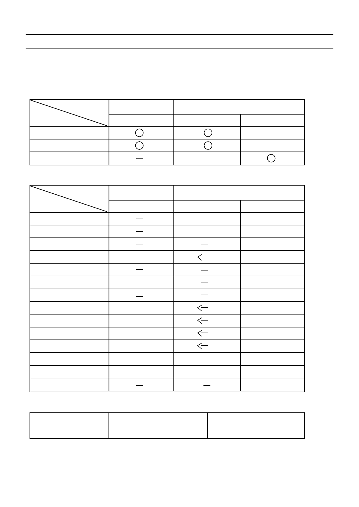
Service manual SC-150
-79-
MICOM/PCB Ver.
Loc
RB02
P502
P503
4959812224-014959812224-00
DW3834-C4-AE2 DW3834-C4-AE2 New Micom(V0.24)
* THE DIFFERENT PART LIST BY PCB & MICOM VERSION
MAIN PCB
X
X
X
I601 MSP3410G-PP-B8-V3 MSP3411G
LOC
DSC-3220E DSC-3220L
MICOM/PCB Ver.
Loc
IT01
JT02
JT03
CT04 25V 47UF
25V 47UF
JUMPER DEL
DEL
JUMPER
DEL
JUMPER
DEL
Z9.1
CXA1315P
JUMPER
CT06
DT01
IT02
RT04
RT08
RT09
RT10
RT11
RT12
RT13
4959812324-014959812324-00
DW3834-C4-AE2 DW3834-C4-AE2 New Micom(V0.25)
UNION PCB
* THE DIFFERENT PART LIST BY MODEL NAME
1/6 3.6K 1/6 3K
1/6 4.7K
1/6 100
1/6 100
1/6 200
1/6 10K
1/6 2.2K
1/6 10K
6-2. Service Parts List option
Page 81
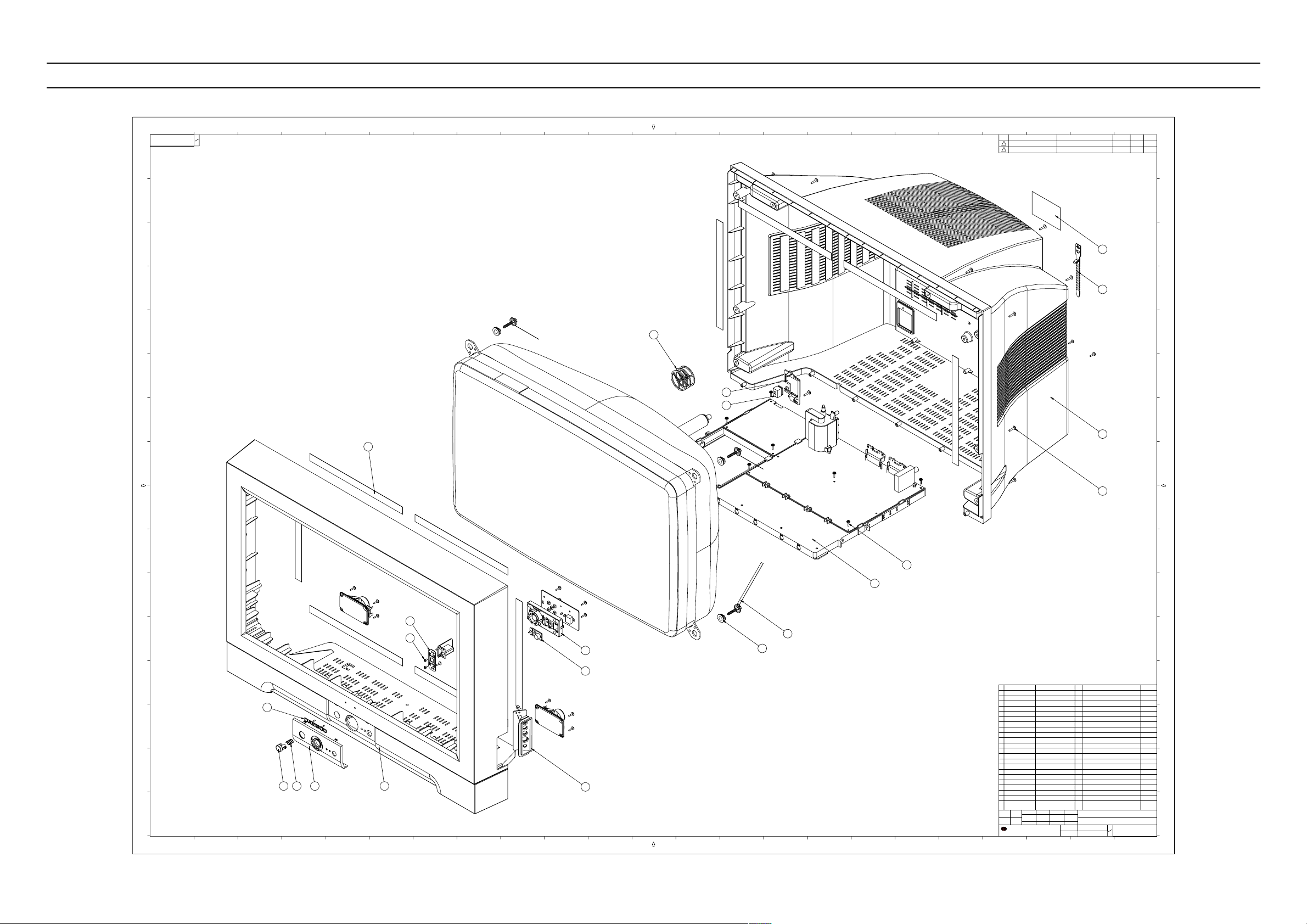
Service manual SC-150
-80-
1
2
3
4
5
6
7
8
9
10
11
12
13
14
15
16
17
18
19
20
21
22
12
12
P
O
N
1
2 3 4
M
L
K
J
I
5 6 7 8 9 10 11
H
G
F
E
D
49500038
C
B
A
D
1
N
2 3 4 5 6 7 8 9 10 11
13 14 15 16 17 18 19
49500038
REMARKS
A0(1189mm X 841mm)
Daewoo Electronics CO.,LTD.
Mechanical Design Team, TV Research
20 21
Center
REFERENCE
22
N
23
Inspected by
BUTTON CH
BUTTON POWER
FRAME MAIN PCB
HOLDER CORD
BRKT POWER
PANEL CTRL
PANEL AV
COVER BACK
MASK FRONT
CLOTH BLACK
CLAMP WIRE
SPRING
WASHER RUBBER
MARK BRAND
HOLDER CORD
HOLDER CORD
PART NAME
4856716000
4856215402
4855617400
4853535600
4853535500
PART CODENO
SCALE
0.5
UNITS
mm
3
2
1
5
4
Checked by
2002. 9. 19
CHO S.J
Designed by
4954901600
4954801000
4953802800
4953500100
4953200600
4952301300
4952300701
4952102200
4952002400
4857817610
4856816300
11
10
8
7
6
9
16
15
14
13
12
EXPLODED VIEW
DSC-3220E
SWPA PIE0.5
CU AU+ABS BK
QTY
MODEL
Approved by
1
1
1
1
4
PART NAME
D
MATERIAL
NYLON 66
NYLON 66
CR T2.0
FR HIPS BK
HIPS PAINT
FELT 300X20X0.7
NYLON 6 (V0)
1
10
1
3
1
1
1
1
1
1
1
FR HIPS
FR HIPS
FR HIPS
EGI T1.2
FR HIPS
FR ABS
FR ABS
P
1(1/ )
O
N
SCREW TAPTITE
SCREW TAPTITE
SCREW TAPTITE
SCREW CRT FIX
DECO SENSOR
SPEC PLATE
7178301212
7172401612
7063300612
4956000100
4955501000
4955400100
22
21
20
19
18
17
TT2 WAS 3X12 MFZN BK
TT2 TRS 4X16 MFZN BK
M/C BIN 3X6 MFZN BK
SWRM10A L=35
PMMA MILKY
PE FILM 91.5X63
27
11
4
1
1
2
M
L
K
J
I
13 14 15 16 17 18 19
H
G
F
E
D
1
2
LIST OF MODIFICATION
20
REV
21
REASON OF MODIFICATION22DATE NAME
23
C
B
A
APPR
7. Explode View
Page 82
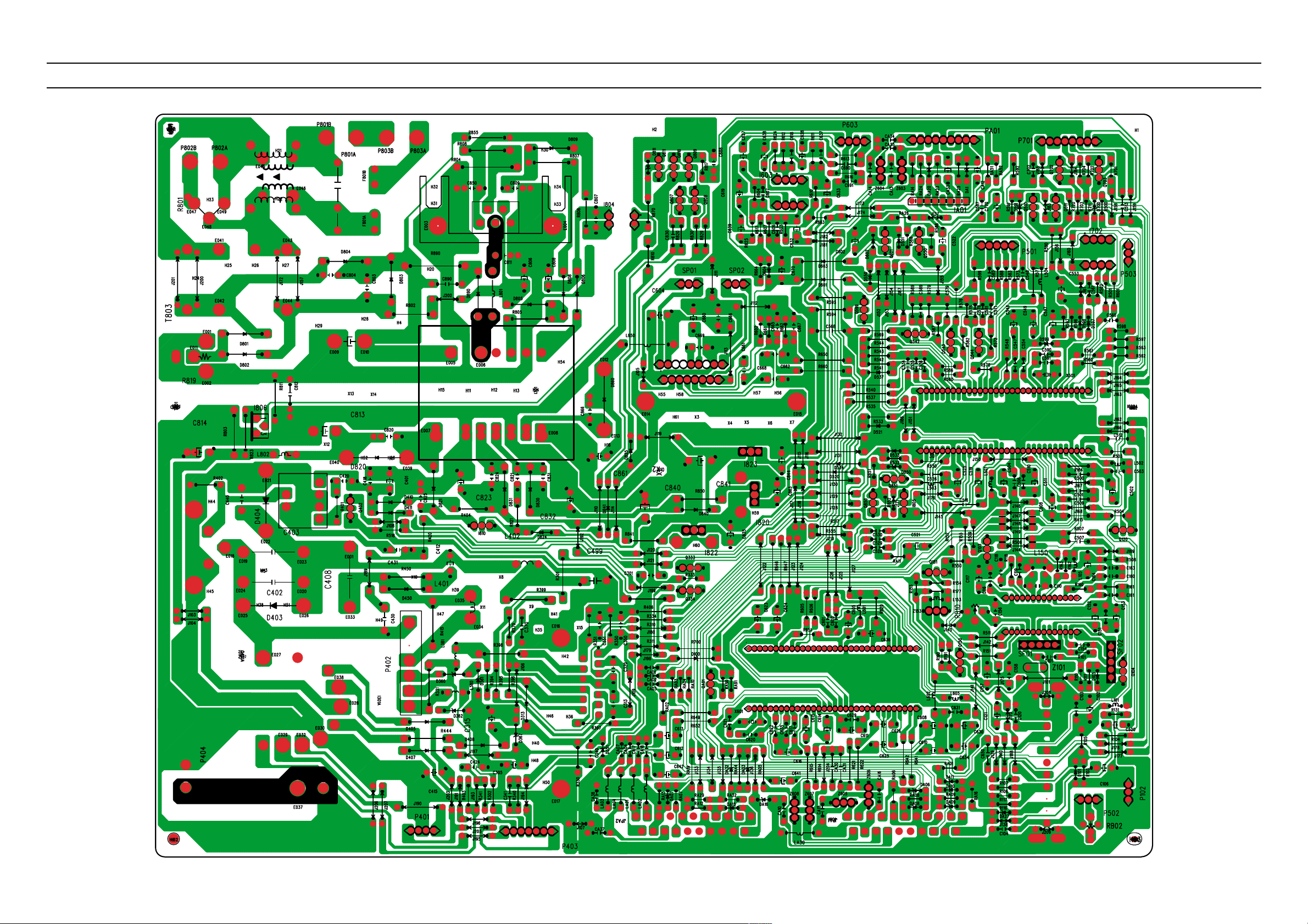
Service manual SC-150
-81-
8-1. PCB MAIN
Page 83
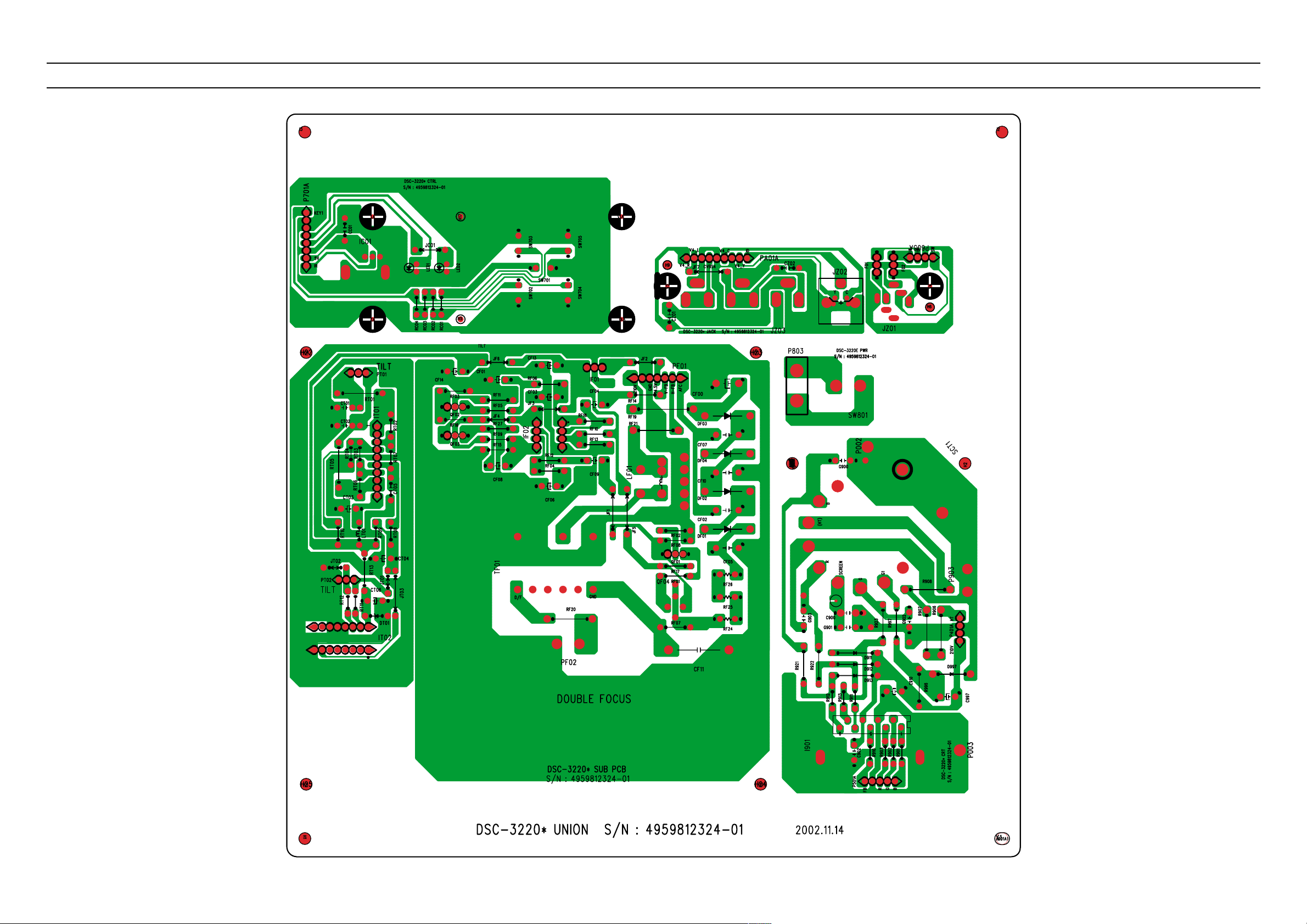
Service manual SC-150
-82-
8-2. PCB UNION
Page 84

Service manual SC-150
-83-
9-1. Schematic Diagram(MAIN
Page 85
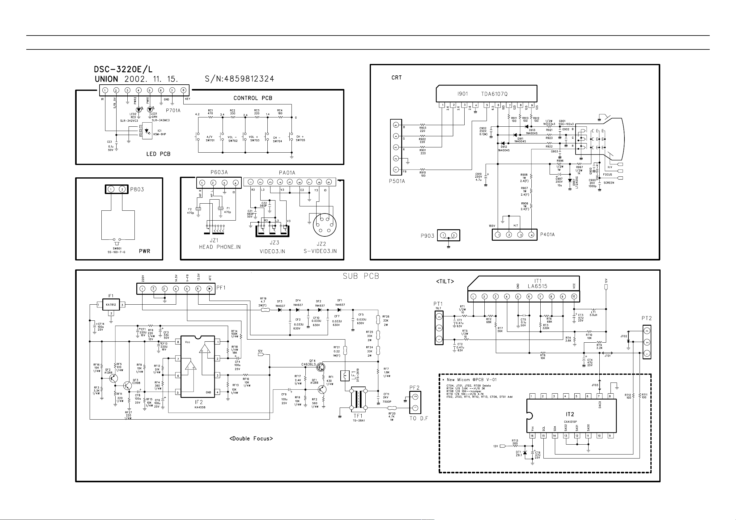
Service manual SC-150
-84-
9-2. Schematic Diagram(UNION)
Page 86

 Loading...