

Page 1

Service Manual
Car Audio
COMPACT DISC CHANGER
MODEL:AKD-80C
DAEWOO ELECTRONICS CO., LTD
Page 2

DAEWOO
CONTENTS
- 1 -
GENERAL SPECIFICATIONS......................................................2
GENERAL....................................................................................3
DISASSEMBLY............................................................................7
DIAGRAMS...................................................................................................10
PARTS LIST.................................................................................................26
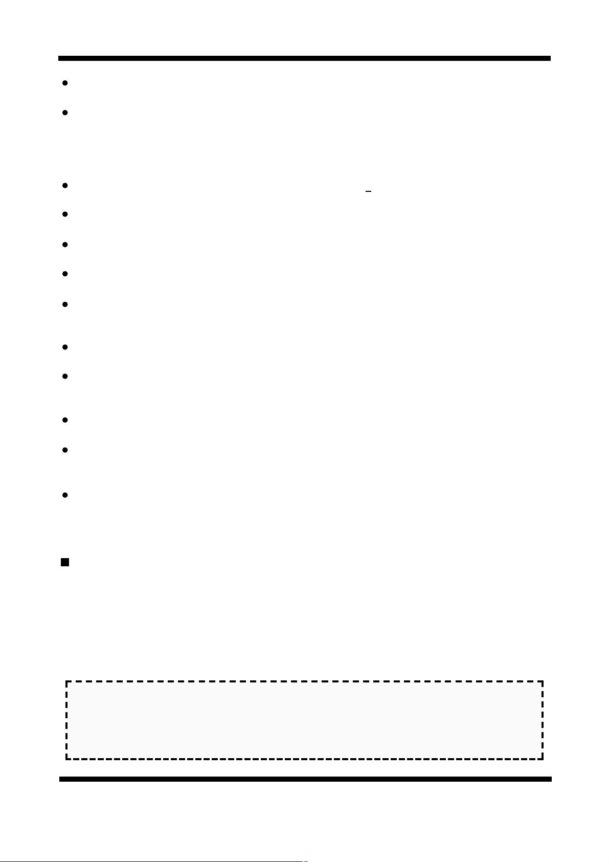
1.IDENTIFICATION OF PARTS...........................................................................3
2.INSTALLATION PARTS AND SUPPLIED MOUNTING HARDWARE...........3~4
3.INSTALLATION METHOD (HOW TO INSTALL THE UNIT)...............................5
4.INSTALLATION METHOD (HOW TO INSTALL THE VEHICLE)........................6
5.PREPARATIONS............................................................................................6
1.DISASSEMBLY..............................................................................................7
2.PICK-UP/MECHANISM/MAGAZINE ASSEMBLY...............................................8
3.IDENTIFICATION OF MAGAZINE.....................................................................9
1.SCHEMATIC DIAGRAM.................................................................................10
2.ELECTRICAL SPECIFICATION........................................................................11
3.MICOM PIN CONFIGURATION & DESCRIPTIONS.................................12~14
4.IC BLOCK DIAGRAM & TERMINAL VOLTAGE........................................15~23
5.PRINTED CIRCUIT BOARDS...................................................................24~25
ELECTRICAL PARTS LIST.....................................................................26~27
Page 3
GENERAL SPECIFICATIONS
DAEWOO
Compact Disc Digital Audio System
Material : GAAIAS
Wavelength : 780nm
Emission Duration : Continuous
Laser Output Power : Less Than 44.6uW
5-20,000Hz + 1dB
Below Measurable Limit
90dB
Line Output (For changer Connector Only)
800mA (CD Play Back)
800mA (During Loading or Ejection a Disc)
-10oC to 55oC (14oF to 131oF)
Appro x 245 x 85 x174mm (W x H x D)
Not lncl. Projection Parts and Control
Approx. 2.3kg
12V DC Car Battery
(Negative Ground)
Disc Magazine (1)
Mounting Hardware(1Set)
Connecting Cable (1)
System
Laser Diode Properties
Frequency Response
Wow and Flutter
Signal-To Noise Ratio
Outputs
Current Drain
Operating Temperature
Dimensions
Weight
Power Requirement
Supplied Accessories
- 2 -
NOTES ON HANDLING THE OPTICAL PICK-UP BLOCK OR BASE UNIT
1. The laser diode in the optical pick-up block may suffer electrostatic breakdown because of the
potential difference generated by the charged electrostatic load, etc. on clothing and the human
body.
2. During repair, pay attention to electrostatic breakdown and also use the procedure in the printed
matter which is included in the repair parts.
3. The flexible board is easily damaged and should be handled with care.
CAUTION :
USE OF CONTROLS, ADJUSTMENTS, OR PERFORMANCE OF PROCEDURES OTHER THAN THOSE SPECIFIED
HEREIN, MAY RESULT IN HAZARDOUS RADIATION EXPOSURE.
THE COMPACT DISC PLAYER SHOULD NOT BE ADJUSTED OR REPAIRED BY ANYONE EXCEPT PROPERLY
QUALIFIED SERVICE PERSONNEL.
Page 4
GENERAL
DAEWOO
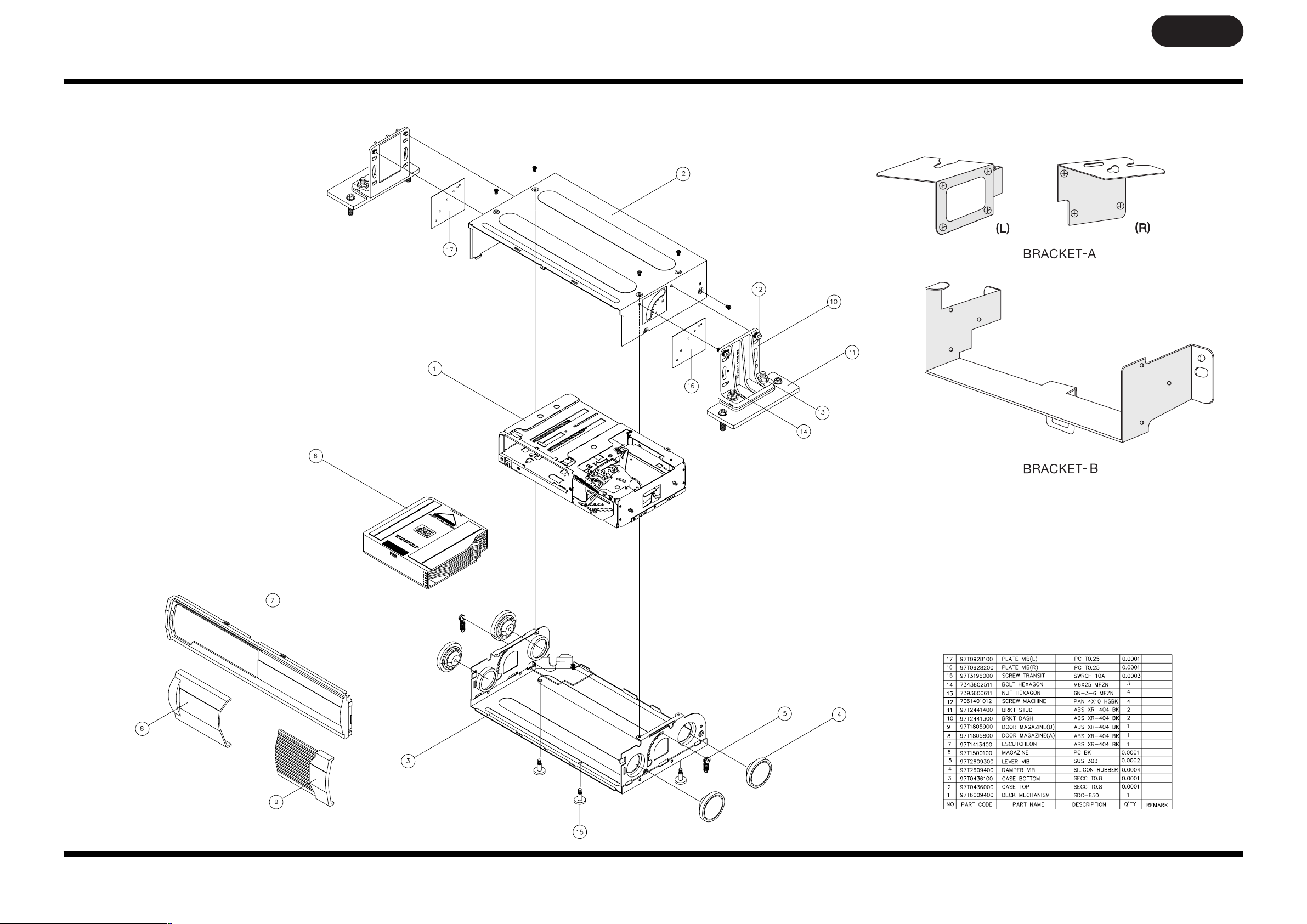
1.IDENTIFICATION OF PARTS
2. INSTALLATION PARTS AND SUPPLIED MOUNTING HARDWARE
- 3 -
Page 5
DAEWOO
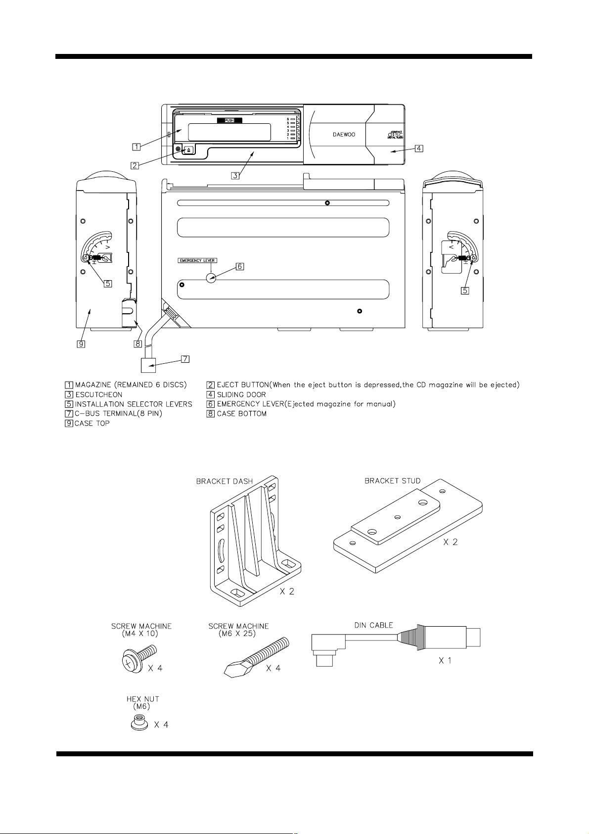
HORIZONTAL POSITION INSTALLATION (WITH BRACKET STUD)
VERTICAL POSITION INSTALLATION
(WITH BRACKET STUD)
HORIZONTAL POSITION INSTALLATION
(WITHOUT BRACKET STUD)
SUSPENDED POSITION INSTALLATION
(WITH BRACKET STUD)
VERTICAL POSITION INSTALLATION
(WITHOUT BRACKET STUD)
- 4 -
Use the wing nut to hold in place the
installation bracket with bolt(M6 x 25) to the
installation bracket, which is attached to the
unit. Then affix the cushion rubber.
Holes with the “H” marks are to be used for
horizontal or suspending and “V” for vertical
installation.
1.
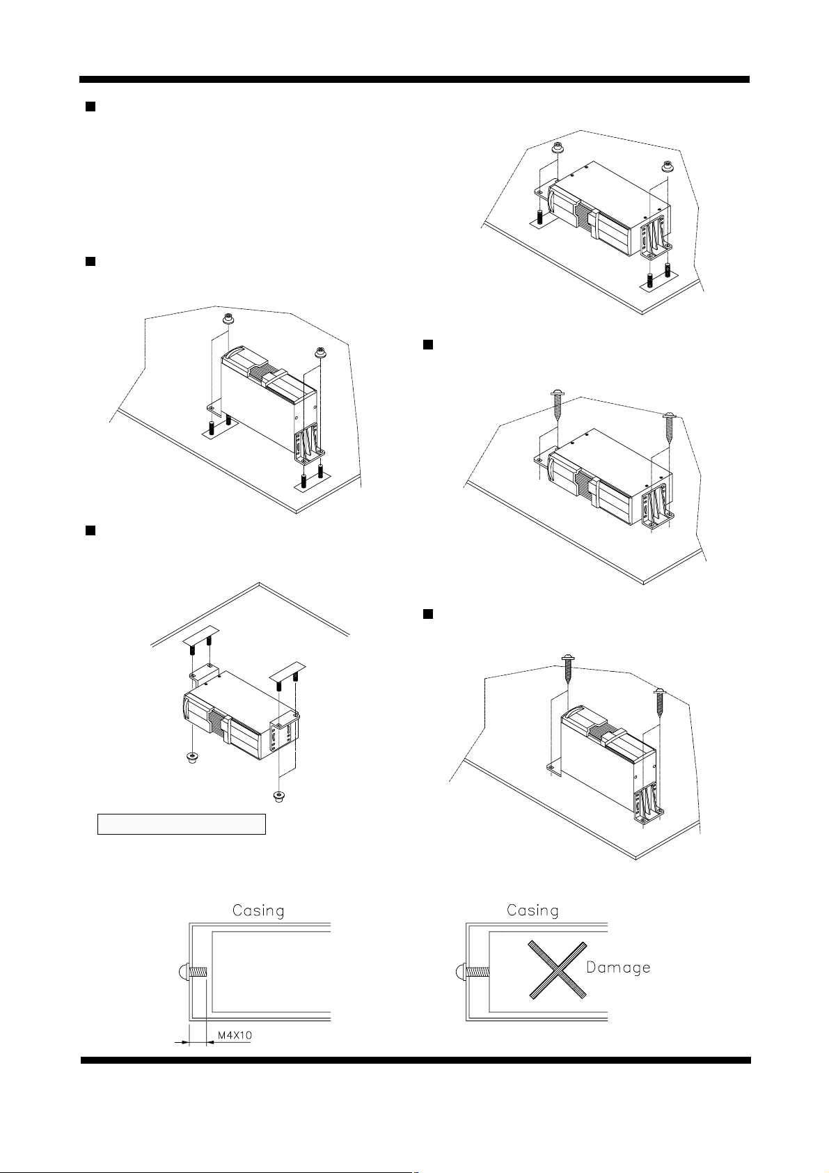
Only the provided screws and brackets should be used during installation. Using
screws other than those specified will cause damage.
2. Before installation, check that there is no harness at the back when making a hole
on the dashboard.
Dangerous Installation
Page 6
DAEWOO
3. INSTALLATION METHOD
(HOW TO INSTALL THE UNIT)
- 5 -
REMOVE TRANSIT SCREW 3 EACH BEFORE INSTALLATION
PART BRACKET DASH(L TYPE) ADHERE TO THE UNIT
After Setting the installation selector levers both sides(left, right)
SETTING THE INSTALLATION SELECTOR LEVERS ADJUST FOR UNIT (PRIOR TO INSTALL)
HORIZONTAL VERTICAL DECLINING
After Select Mark Hole(1), (2), (3)
The unit fasten by the screw(M4 x 10)
After Select Mark Hole (4)
The unit fasten by the screw(M4 x10)
After Select Mark Hole (2)
The unit fasten by the screw(M4 x 10)
Page 7

DAEWOO
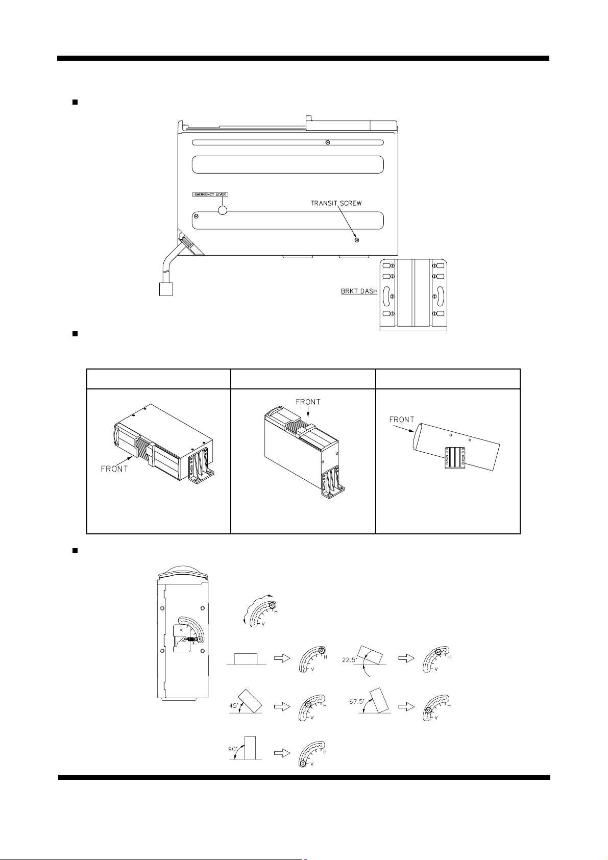
4.INSTALLATION METHOD
(HOW TO INSTALL THE VEHICLE)
5.PREPARATIONS
- 6 -
Should be determined before the unit install under
carpet.
Adjust the installation bracket with bolts to suit the place
of installation.
1.Remove the floor carpet and decide on the place to
install.
2.Remove the separator of the cushion rubber that is
attached to the installation bracket with bolt and install
accordingly.
3.Align the unit with the bolts and secure it with the wing
nuts.
1.USAGE OF MAGAZINE (To load the discs)
Load the discs with the labels facing upwards, as
shown in the diagram.
2.TO LOAD THE MAGAZINE
Slide the sliding door to the right until it is completely
latched on.
Load the magazine in the direction as shown in the
diagram. push it in until is locked into the unit.
After the magazine has been loaded, close the sliding
door.
(If not close sliding door, Dirt or dust entering it will
cause damage)
3.TO REMOVE THE MAGAZINE
Open the sliding door and depress the eject button.
Remove the magazine when it has been ejected.
Close the sliding door.
Notes on handling the optical pick-up block or base unit
1.The laser diode in the optical pick-up block may suffer
electrostatic breakdown because of the potential
difference generated by the charged electrostatic
load,etc. on clothing and the human body.
2.During repair, pay attention to electrostatic breakdown
and also use the procedure in the printed matter which
is included in the repair parts.
3.The flexible board is easily damaged and should be
handled with care.
CAUTION:
USE OF CONTROLS, ADJUSTMENTS, OR PERFORMANCE OF PROCEDURES OTHER THAN
THOSE SPECIFIED HEREIN, MAY RESULT IN HAZARDOUS RADIATION EXPOSURE.
THE COMPACT DISC PLAYER SHOULD NOT BE ADJUSTED OR REPAIRED BY ANYONE
EXCEPT PROPERLY QUALIFIED SERVICE PERSONNEL.
Page 8
DISASSEMBLY
DAEWOO
1. DISASSEMBLY
- 7 -
Size:A3
Page 9
DAEWOO
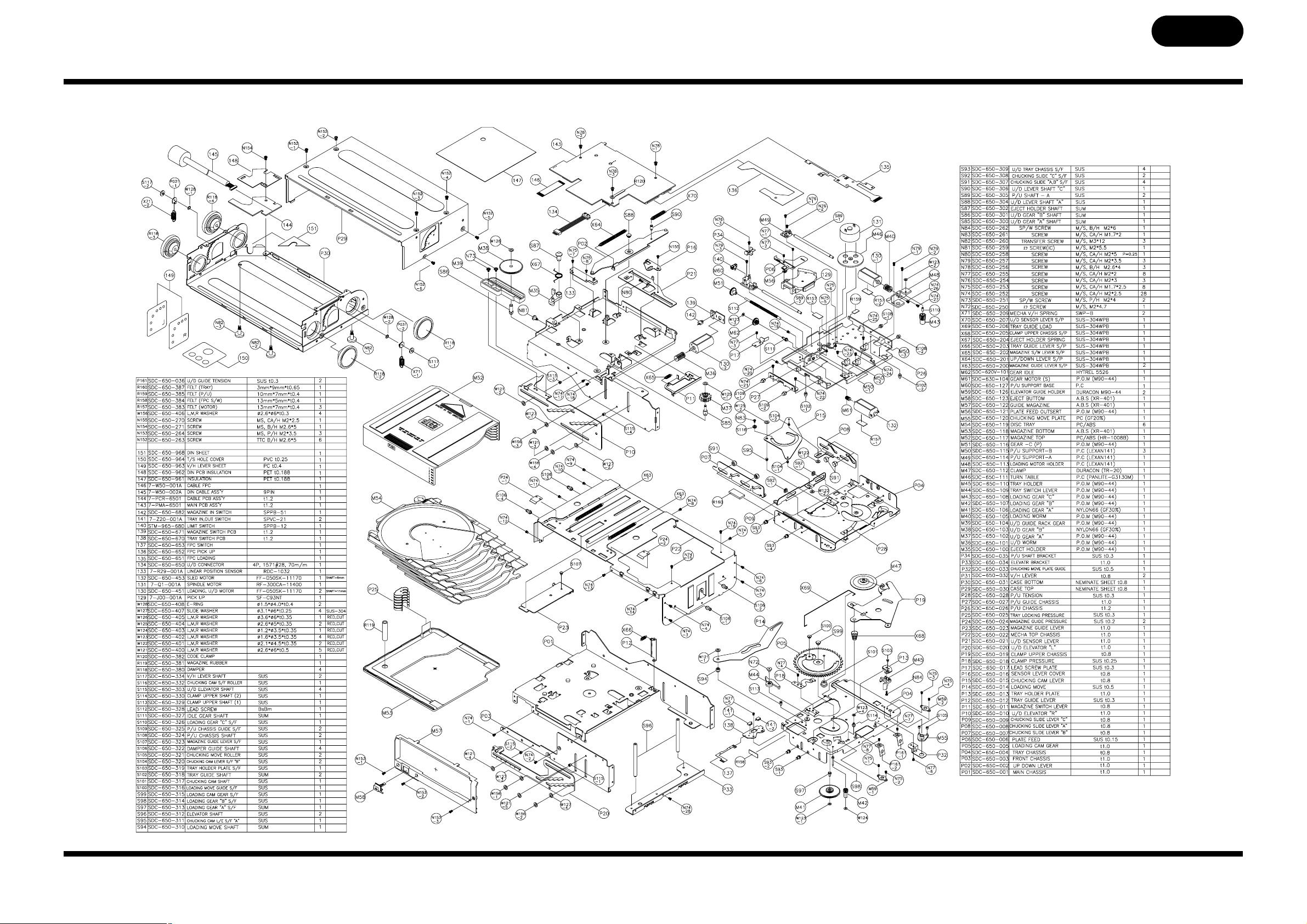
2. PICK-UP/MECHANISM/MAGAZINE ASSEMBLY
- 8 -
Size:A3
Page 10

DAEWOO
3. IDENTIFICATION OF MAGAZINE
- 9 -
Page 11

DIAGRAMS
DAEWOO
1. SCHEMATIC DIAGRAM
- 10 -
Size:A3
Page 12

DIAGRAMS
DAEWOO
2.ELECTRICAL SPECIFICATION
TEST DISC : SONY YEDS 18 TYPE 4 OR TCD-784
PLAY ABILITY TEST (25oC)
- 11 -
NO
ITEM
TEST
CONDITION
UNIT NOMINAL LIMIT 1 2 REMARK
1
2
3
4
5
6
7
8
20Hz
100Hz
dB
dB
dB
dB
dB
dB
V
mA
%
10KHz
20KHz
1KHz
-2.6
0.01
4dB
2dB
2dB
3dB
80dB
75dB
3dB
3dB
70dB
60dB
0.8 0.1
<5mA
0.3%
JIS A
FILTER
JIS A
FILTER
JIS A
FILTER
JIS A
FILTER
JIS A
FILTER
-0.3
-1.3
90
90
0.07
20dB
20dB
86
76
2.7
FREQUENCY RESPONSE
S/N RATIO
DYNAMIC RANGE
T.H.D
DE-EMPHASIS
CHANNEL SEPARATION
OUTPUT LEVEL (V)
BACK UP CURRENT(mA)
5KHz
16KHz
1KHz
10KHz
1KHz
L
R
L
R
ITEM
FINGER PRINTS
ECCENTRICITY DISC
VERTICAL DEVIATION DISC
SCRATCH DISC
INTERRUPTION DISC
TEST CONDITION
BLACK DOT
A-BEX TCD-721R
A-BEX TCD-725A
A-BEX TCD-725A
A-BEX TCD-725A
A-BEX TCD-713
A-BEX TCD-731R
LIMIT
600uM
700uM
600uM
65uM
210uM
1000uM
< +
< +
< +
< +
<
>
>
> +
> +
+
+
+
Page 13

3. MICOM PIN CONFIGURATION & DESCRIPTIONS
DAEWOO
PIN CONFIGURATIONS (LC865016B-XXXX)
- 12 -
Page 14

DAEWOO
PIN DESCRIPTION
- 13 -
PIN
No
FUNCTION
D-GND
DATA
DATA
EJECT
D-GND
D-GND
TEST
ACC
STBY
D-GND
D-GND
TEST
SL +
OPTION
SLED MOTOR Control Pulse
SLED MOTOR Control Pulse
1
2
3
4
5
6
7
8
9
10
11
12
13
PIN
NAME
P70
P71
P72
P73
P30
P31
P32
P33
P34
P35
P36
P37
P40
I/O
I/O
I
I
I
I/O
I/O
I/O
I/O
I/O
I/O
I/O
I/O
I/O
SL -
14
P41
I/O
D-GND15
P42
I/O
PLAY MODE (L)
S-MUTE16
P43
I/O
A-MUTE17
P44
I/O
POWC18
P45
I/O
D-GND19
P46
I/O
D-GND20
P47
I/O
SUBQ DATA SYNC DETECTOR
FSEQ21
P50
I/O
FOCUS OK SIGNAL IN
DRF22
P51
I/O
VSS POWER PIN(-)
23
VSS
VDD/VPP POWER
PIN(+)
24
VDD/
VPP
IN SW
25
P20
I/O
I/O
I/O
I/O
I/O
I/O
I/O
I/O
PULL UP (22K)
PULL UP (22K)
PULL UP (22K)
PULL UP (22K)
PULL UP (47K)
PULL UP (47K)
PULL UP (47K)
LOAD SW
26
P21
HOME SW
27
P22
M SW
28
P23
P24
29
P24
DOK
30
P25
DISK P
31
P26
LOAD P
32
P27
Page 15

DAEWOO
- 14 -
PIN DESCRIPTION
PIN
No
FUNCTION
SK
COIN
SQOUT
CQCK
RWC
WRQ
TEST
DO
XT1
XT2
VSS POWER PIN (-)
OPTION
41
42
43
44
45
46
47
48
49
50
51
52
PIN
NAME
P11
P12
P13
P14
P15
P16
P17
TEST1
XT1/
P74
XT2
VSS
I/O
I/O
I/O
I/O
I/O
I/O
I/O
I/O
O
RES REST PINRES
I
I
O
CF1
53
CF1
I
CF2
54
CF2
O
CONNECT TO VS1(VDD)
VDD POWER PIN (+)
55
VDD
PULL-UP (10K)
56
P80
AD INPUT PORT
AD INPUT PORT
AD INPUT PORT
AD INPUT PORT
AD INPUT PORT
AD INPUT PORT
AD INPUT PORT
AD INPUT PORT
57
P81
58
P82
59
P83
60
P84
61
P85
62
P86
63
64
P87
I
I
I
I
I
I
I
I
PULL UP (10K)
I/O
DI
P10
I/O
LOAD
33
P00
I/O
E-UP
34
P01
I/O
E-DN
UNLOAD
35
P02
I/O
D-GND
36
P04
I/O
D-GND
37
P05
I/O
XRST
38
P06
I/O
CS
39
P07
40
Page 16

4. IC BLOCK DIAGRAM & TERMINAL VOLTAGE
DAEWOO
IC 101(LA9240M) -RF+ASSP+AUDIO FILTER
- 15 -
1. PIN CONFIGURATION
2. BLOCK DIAGRAM
Page 17

3. TERMINAL VOLTAGE & DESCRIPTION
DAEWOO
- 16 -
PIN
No
Pickup photodiode connection pin. Added to FIN1 pin to generate the RF signal, subtracted
from FIN1 pin to generate the FE signal.
1
FIN2
Pickup photodiode connection pin.2 FIN1
SYMBOL
CONTENTS
Pickup photodiode connection pin. Subtracted from F pin to generate the TE signal.3E
Pickup photodiode connection pin.4F
TE signal DC component input pin.5TB
Pin which connects the TE signal gain setting resistor between this pin and TE pin.6 TE
-
TE signal output pin.7TE
TES(Track Error Sense) comparator input pin. The TE signal is input through a band pass filter.
8 TESI
Shock detection input pin.9 SCI
Tracking gain time constant setting pin.10 TH
TA amplifier output pin.11 TA
Pin for configuring the tracking phase compensation constant between the TD and VR pins.
12 TD
-
Tracking phase compensation setting pin.13 TD
Tracking jump signal (kick pulse) amplitude setting pin.14 JP
Tracking control signal output pin.15 TO
Focusing control signal output pin.16 FD
Pin for configuring the focusing phase compensation constant between the FD and FA pin.
Pin for configuring the focusing phase compensation constant between the FD
-
and FA-pin.
Pin for configuring the focusing phase compensation constant between the FA and FE pin.
17 FD
-
18 FA
19 FA
-
FE signal output pin.20 FE
Pin which connects the FE signal gain setting resistor between this pin and FE pin.21 FE
-
Analog signal GND.22 AGND
CV+ and CV -pins input signal single-end output.23 SP
Spindle amplifier input.24 SPI
12-cm spindle mode gain setting resistor connection pin.25 SPG
Spindle phase compensation constant connection pin, along with the SPD pin.26 SP
Spindle control signal output pin.27 SPD
Sled phase compensation constant connection pin.28 SLEQ
Sled control signal output pin.29 SLD
Input pin for sled movement signal from microprocessor.30 SL
-
Input pin for sled movement signal from microprocessor.SL
+
31
Input pin for tracking jump signal from DSP.32 JP
Input pin for tracking jump signal from DSP.JP
+
33
Input pin for tracking gain control signal from DSP. Gain is low when TGL is high.
Input pin for tracking off control signal from DSP. Tracking servo is off when TOFF is high.
34 TGL
35 TOFF
Output pin for TES signal to DSP.36 TES
The High Frequency Level is used to determine whether the main beam is positioned over a
bit or over the mirrored surface.
37 HFL
Sled servo off control input pin.38 SLOF
Input pin for CLV error signal from DSP.
Input pin for CLV error signal from DSP.
39
CV
-
40
CV
+
Page 18

DAEWOO
- 17 -
PIN
No
RF output pin.
41
RFSM
RF gain setting and EFM signal 3T compensation constant setting pin, along with the RFSM pin.
42
RFS
-
Slice Level Control is an output pin that controls the data slice level used by the DSP for the
RF wave form.
43 SLC
SYMBOL
CONTENTS
Input pin used by DSP for controlling the data slice level.44 SLI
Digital system GND pin.45 DGND
Focus search smoothing capacitor output pin.46 FSC
Tracking balance control, EF balance adjustment variable range setting pin.47 TBC
No connection
48 NC
Disc defect detection output pin.49 DEF
Reference clock input pin. 4.23 MHz signal from the DSP is input.50 CLK
Microprocessor command clock input pin.51 CL
Microprocessor command data input pin.52 DAT
Microprocessor command chip enable input pin.53 CE
RF level detection output (Detect RF)54 DRF
Focus search select; focus search mode (+search/+search vs. the reference voltage)
switching pin
55 FSS
Servo system and digital system VCCpin.
By-pass capacitor connection pin for reference voltage.
Reference voltage output pin.
56 VCC2
VCC1
57
REFI
58 VR
Disc defect detection time constant setting pin.59 LF2
RF signal peak hold capacitor connection pin.
RF signal bottom hold capacitor connection pin.
60 PH1
61 BH1
APC circuit output pin.
APC circuit input pin.
62 LDD
63 LDS
RF system V
CC
pin.64
Page 19

DAEWOO
- 18 -
IC 501 (LB 1836) - 2CH. Bidirectional Motor Driver IC
1. PIN CONFIGURATION
2. BLOCK DIAGRAM
Page 20

DAEWOO
IC 201(LC 78626) - DSP for CDP
- 19 -
1. PIN CONFIGURATION
2. BLOCK DIAGRAM
Page 21

DAEWOO
3. TERMINAL VOLTAGE & DESCRIPTION
- 20 -
Defect detection signal(DEF)input. When not used,must be connected to 0V
For the PLL
Test input.Equipped with internal pull-down resistor.Must be connected to 0V
External VCO control phase comparator output
Internal VCO ground.Must be connected 0V
PDO output current adjustment resistor connection
Internal VCO power supply
VCO frequency range adjustment
Digital system ground. Must be connected to 0V
Test operation mode control input.Must be connected to VDD.
Test operation mode control input.Must be connected to VDD.
Test operation mode control input.Must be connected to VDD.
Test operation mode control input.Must be connected to VDD.
Test operation mode control input.Must be connected to VDD.
Test input.Equipped with internal pull-down resistor.Must be connected to 0V
Chip select input.Equipped with internal pull-down resistor.
When not controlled,must be connected to 0V
Test input. Must be connected to 0V
For slice
level control
EFM signal output
EFM signal input
Test input.Equipped with internal pull-down resistor.Must be connected to 0v
Disk motor control output.Can have a 3-state output depending on the
command
Rough servo/phase control automatic switching monitor output.If a high level then
rough servo mode.If a low level then phase control mode.
Track detect signal input.Schmidt input.
Tracking error signal input.Schmidt input.
Tracking off output.
Tracking gain switch output.Gain is increased with low level
Track jump control output.Can be 3-state output depending on the command.
EFM data playback clock monitor. 4.3218 MHz during phase lock.
Sync signal detect output.A high level when the sync signal detected from the EFM
signal matches the internally generated sync signal.
Digital system power supply.
Reset signal input for initializing only the anti-shock control part.(i.e. excluding the
DSP part.)Resets when this pin is low level,and release the reset when this pin is
high level.Tie this pin to the low level.(i.e.connected to 0V)if when using software
control on the anti-shock part alone through the anti-shock part only reset
disable/release command($f4) or the anti-shock only reset enable/inrush
command($f5).
Note:This pin is assigned as the least significant bit of the general I/O port however,
use as a general I/O pin is disabled.When the port I/O set command($DB) is
executed.The least significant bit is always “0”,and the output driver is not turned
ON.
1
2
3
4
5
6
7
8
9
10
11
12
13
I
O
P
AI
P
AI
P
I
I
I
I
I
I
I
I
O
I
I
O
O
O
I
I
O
O
O
O
O
O
P
I(I/O)
DEFI
TAI
PDO
VV
ss
ISET
VV
DD
FR
V
ss
TESCLK
TESA
TESB
TESC
TESGB
TEST5
CS
TEST1
EFMO
EFMI
TEST2
CLV
+
CLV
-
V/P
HFL
TES
TOFF
TGL
JP
+
JP
-
PCK
FSEQ
V
DD
ASRES
14
15
16
17
18
19
20
21
22
23
24
26
28
29
30
31
32
25
27
PIN
No
PIN
NAME
I/O FUNCTION
I
Page 22

DAEWOO
- 21 -
General I/O pin 2.This controls the commands from the microcontroller.When not
used,either set this as an input port and connect to 0V, or set this as an output port
and leave it open.
I/O
CONT2
33
PIN
No
General I/O pin4.This controls the commands from the microcontroller.This pin is
shared exclusively with the sub code frame sync signal output(SFSY).When not
used,either set this as an input port and connect to 0V,or set this as an output port
and leave it open.
General I/O pin4.This controls the commands from the microcontroller.This pin is
shared exclusively with the sub code P,Q,R,S,T,U,V,W output(PW).When not
used,either set this as an input port and connect to 0V,or set this as an output port
and leave it open.
General I/O pin3.this controls the commands from the microcontroller.This is
shared exclusively with the sub code read clock input(SBCK).When not
used,either set this as an input port and connect to 0V, or set this as an output port
and leave it open.
16.9344 MHz output
4.2336 MHz output
Digital output EIAJ format.
Test input.Equipped with internal pull-down resistor.Must be connected to 0v
G1,G2,one error, two error correction monitor output
7.35KHz sync signal output(frequency divided from the crystal oscillator)
Sub code block sync signal output
Test input.Equipped with internal pull-down resistor.Must be connected to 0v
Deemphasize monitor output.When high level, a deemphasize disc is being played back.
G2 flag output
Tracking error Test output.Under normal operation ,this should be left open.
DRAM switch:high: 1M, low:4M
Test input.Must be connected to 0V
Test input.Must be connected to 0V
L channel mute output
L channel power supply
L channel output
L channel ground.Must be connected to 0V
R channel output
R channel power supply
R channel mute output
Crystal oscillator power supply
16.9344 MHz crystal oscillator connection.
Crystal oscillator ground. Must be connected to 0V
Read/write control input.Schmidt input.
Microcontroller command input.
34
CONT3/
SBCK
I/O
35
36
37
PIN NAME I/O
I/O
I/O
O
I
O
I
O
O
O
O
O
O
O
I
I
I
O
P
AO
P
AO
P
O
P
O
I
P
I
I
FUNCTION
CONT4/
SFSY
CONT5/
PW
SBSY
TEST3
DOUT
TEST4
16M
4.2M
EFLG
FSX
EMPH
C2F
TOUT
MR1
TESE
TESD
MUTESL
LVdd
For the one-bit
D/A converter
LCHO
L/RVss
RCHO
RVdd
MUTER
XVDD
XOUT
XIN
XVSS
RWC
COIN
38
39
40
41
42
43
44
45
46
47
49
51
52
53
54
55
56
57
58
59
60
61
62
63
48
50
Page 23

DAEWOO
- 22 -
PIN
No
DRAM address bus
DRAM address bus
DRAM address bus
DRAM address bus
DRAM address bus
Remaining DRAM output
Remaining DRAM output
Remaining DRAM output
DRAM write terminated. (An RZP pulse is output when there is an overflow or a shock.))
Data contact point detection complete signal:low->high:detection complete(DRAM write start)
DRAN write enable signal input: high:write enable
Pause signal input : high :pause
C2F data contact point detection start signal : low -> high:detection start
Remaining DRAM alarm output: low : memory low
C2F shock detect pause signal input : low : pause shock detection
DRAM data bus
DRAM data bus
DRAM data bus
DRAM data bus
DRAM control signal
DRAM control signal
DRAM control signal
DRAM control signal
Digital system ground. Must be connected to 0V
DRAM address bus
DRAM address bus
DRAM address bus
DRAM address bus
DRAM address bus
Digital system power supply
71
72
73
74
75
76
77
78
79
80
81
82
83
84
85
86
87
88
89
PIN NAME I/O
O
O
O
I
I
O
O
I
I/O
I/O
I/O
I/O
O
O
O
O
O
O
O
O
O
P
O
O
O
O
O
P
FUNCTION
MMC1
MMC2
MMC3
OVF
CNTOK
WOK
PAUSE
NGJ
EMPN
SHOCK
DRAM3
DRAM2
DRAM1
DRAM0
OE
WE
CAS
RAS
AD9
AD8
AD7
AD6
AD5
Vss
AD4
AD3
AD2
AD1
AD0
Vdd
90
91
92
93
94
95
96
98
99
100
97
Sub code Q output standby output
Operating mode switch: high:shock proof, low:through
DRAM empty(an RZP pulse is output when the DRAM is empty.
External reset input: low reset(all internal blocks are reinitialized)
Remaining DRAM
O
I
O
I
O
WRQ
FMT
EMPP
RES
MMC0
66
67
68
69
70
Input pin for the command input latch clock and the sub code readout clock.Schmidt
input.
Sub code Q output
I
O
CQCK
SQOUT
64
65
Page 24

DAEWOO
IC 401 (BA6790FP) - 4CH. BTL driver for CDP
1. PIN CONFIGURATION
- 23 -
2. BLOCK DIAGRAM
PIN
No
FUNCTION
Driver channel 1 negative output
Driver channel 1 positive output
Driver channel 1 input
Driver channel 1 input,gain adjustment pin
Connect external transistor base
constant voltage output,connects to
external transistor collector
Mute control pin
Ground
Driver channel 2 input,gain adjustment pin
Driver channel 2 input
Driver channel 2 positive output
Driver channel 2 negative output
Substrate ground
Operational amplifier output
15 OP IN(-)
OP IN(+)
VO3(-)
VO3(+)
VIN3
VIN3
+
Vcc
Vcc
BIAS IN
VIN4
+
VIN4
VO4(+)
VO4(-)
GND
16
17
18
19
20
21
22
23
24
25
26
27
28
1
2
3
4
5
6
7
8
9
10
11
12
PIN
NAME
VO1(
-
)
PIN
No
FUNCTION
PIN
NAME
VO1(+)
VIN1
VIN1
+
REG-B
REG
OUT
MUTE
GND
VIN2
+
VIN2
VO2(+)
VO2(-)
GND
OP OUT
13
14
Operational amplifier input,negative
Operational
amplifier input,positive
Driver channel 3 negative output
Driver channel 3 positive output
Driver channel 3 input
Driver channel 3 gain adjustment pin
Power supply
Power supply
Bias amplifier input
Driver channel 4 gain adjustment pin
Driver channel 4 input
Driver channel 4 positive output
Driver channel 4 negative output
Substrate ground
Page 25

DAEWOO
5. PRINTED CIRCUIT BOARDS
TOP VIEW
- 24 -
Page 26

DAEWOO
BOTTOM VIEW
- 25 -
Page 27

DAEWOO
ELECTRICAL PARTS LIST
- 26 -
IC LC865016B-XXXX
IC LC78626E
IC LA9240M
TR DTC114YK
TR DTA123YK
TR DTC323TK
TR 2SB1238
TR KSD1691Y
CHARGE 0.047F/5.5V
ELEC 100/10V
ELEC 220/10V
ELEC 10/16V
ELEC 47/16V
ELEC 1000/16V
ELEC 4.7/16V
ELEC 0.22/50V
ELEC 0.33/50V
ELEC 0.47/50V
ELEC 1/50V
ELEC 2.2/50V
CHIP C5R0(2012)
CHIP C120(2012)
CHIP C100(2012)
CHIP C300(2012)
CHIP C101(2012)
CHIP C151(2012)
CHIP C331(2012)
CHIP C102(2012)
CHIP C332(2012)
IC301
IC201
IC101
IC LB1836M
IC501
IC BA6790FP
IC401
IC KIA7025F IC302
IC BA178M05FP IC701
TR 2SA1037K
Q101
Q705
TR DTC143EK
Q302, Q703
Q303, Q702
TR DTC143TK Q603
Q601, Q602
Q401, Q704
Q701
C137, C209, C308, C402
C713
C709
C206, C401, C706
C126, C127, C133, C619
C620
ELEC 22/16V C705
C119, C135, C707
C703
C125
C115
C131
C130
C301, C305
C118, C302, C613, C614
C122, C211
C121
C210
C205
C116
C110, C204
C105
C123, C136, C304, C621
C622, C623, C624, C712
C102, C106, C117
DESCRIPTION
REF - NO
DESCRIPTION
CHIP C333(2012)
CHIP C473(2012)
CHIP C104(2012)
C124
C107, C108
C101, C103, C104, C109
C111, C128, C132, C134
C201, C202, C203, C207
C208, C212, C303, C306
C307, C403, C501, C502
C618, C701, C702, C801
C625, C404
CHIP C103(2012)
CHIP C223(2012)
C113, C114, C120, C129
C138
C112, C704, C710, C711
[CAPACITOR]
DESCRIPTION REF - NO
PAST LIST
REF - NO
[I C]
DESCRIPTION
[TRANSISTOR]
Page 28

[DIODE]
[OTHERS]
[RESISTOR]
DAEWOO
- 27 -
DESCRIPTION
CHOKE TRANS EX-19/3mH
WAFER 18P
CONNECTOR 9P
CONNECTOR 4P
8P DIN PLUG(250
mm
)
PCB-MAIN / FR-4 135 x 111
mm
T=1.2
PCB-CONTROL / FR-4 50 x 39
mm
T=1.2
FFC 11P / 11P x 120mm(UL20696) CARD CABLE
REF - NO
CRYSTAL 16.9344
MHz
C-RESONATOR CST 12.0MTW XT301
XT201
L701
SWITCH EJECT (SKQNAB) SW301
JN101
WAFER 11P JN102, JN104, CON101
CON102
JN103
CHIP R=220 (2012)
CHIP R=1 (2012)
CHIP R=270 (3216)
ZENER DIODE 8.2V-C
CHIP DIODE DAN202K
RECT DIODE 1N4004A
DESCRIPTION
REF - NO
R102, R123, R124
R206
R705, R709
D301
CHIP DIODE DA204K D701
ZENER DIODE 5.6V-C ZD703
ZD702
ZENER DIODE 5.1V-B ZD701
CHIP DIODE DAP202K D303
D702, D703
DESCRIPTION
REF - NO
CHIP R=10 (2012)
CHIP R=100 (2012)
CHIP R=330 (2012)
CHIP R=220 (2012)
CHIP R=680 (2012)
CHIP R=1.8 (2012)
CHIP R=2.2 (2012)
CHIP R=3.9 (2012)
CHIP R=4.7 (2012)
CHIP R=5.6 (2012)
CHIP R=6.8 (2012)
CHIP R=8.2 (2012)
CHIP R=10 (2012)
CHIP R=12 (2012)
CHIP R=15 (2012)
CHIP R=18 (2012)
CHIP R=20 (2012)
CHIP R=22 (2012)
CHIP R=33 (2012)
CHIP R=39 (2012)
CHIP R=47 (2012)
CHIP R=56 (2012)
CHIP R=68 (2012)
CHIP R=100 (2012)
R133, R134
CHIP R=0 (2012) R117, R315
CHIP R=47 (2012) R708
R706
R107, R119, R125
R132
R201
CHIP R=1 (2012) R311, R703
CHIP R=1.2 (2012) R122
R619, R620
R110, R115, R704
R104
R105, R205
CHIP R=5.1 (2012) R202
R131
R707
R103, R404
R126, R128, R621
R116
R112, R401, R402, R405
R109, R121
R127
R106, R113, R129, R301
R304, R702
R204, R305
R111
R114, R306, R308, R309
R310, R313, 403
R118, R120, R130
R203
R101, R108, R307, R622
R623
Page 29

DAEWOO ELECTRONICS CO., LTD
99120
 Loading...