

CYStech MTNN20N03Q8 Schematic [ru]
CYStech Electronics Corp.
N-CHANNEL ENHANCEMENT MODE POWER MOSFET
Spec. No. : C805Q8
Issued Date : 2009.12.30
Revised Date :2011.03.21
Page No. : 1/9
MTNN20N03Q8
N-CH 1 N-CH 2
BVDSS 30V 60V
ID 8A 0.115A
Description
The MTNN20N03Q8 provides the designer with the best combination of fast switching, ruggedized device
design, low on-resistance and cost effectiveness.
The SOP-8 package is universally preferred for all commercial-industrial surface mount applications and
suited for low voltage applications such as DC/DC converters.
Features
Simple drive requirement
•
Low on-resistance
•
Fast switching speed
•
Two N-ch MOSFETs in a package
•
Pb-free lead plating package
•
RDSON(MAX)
20mΩ 5Ω
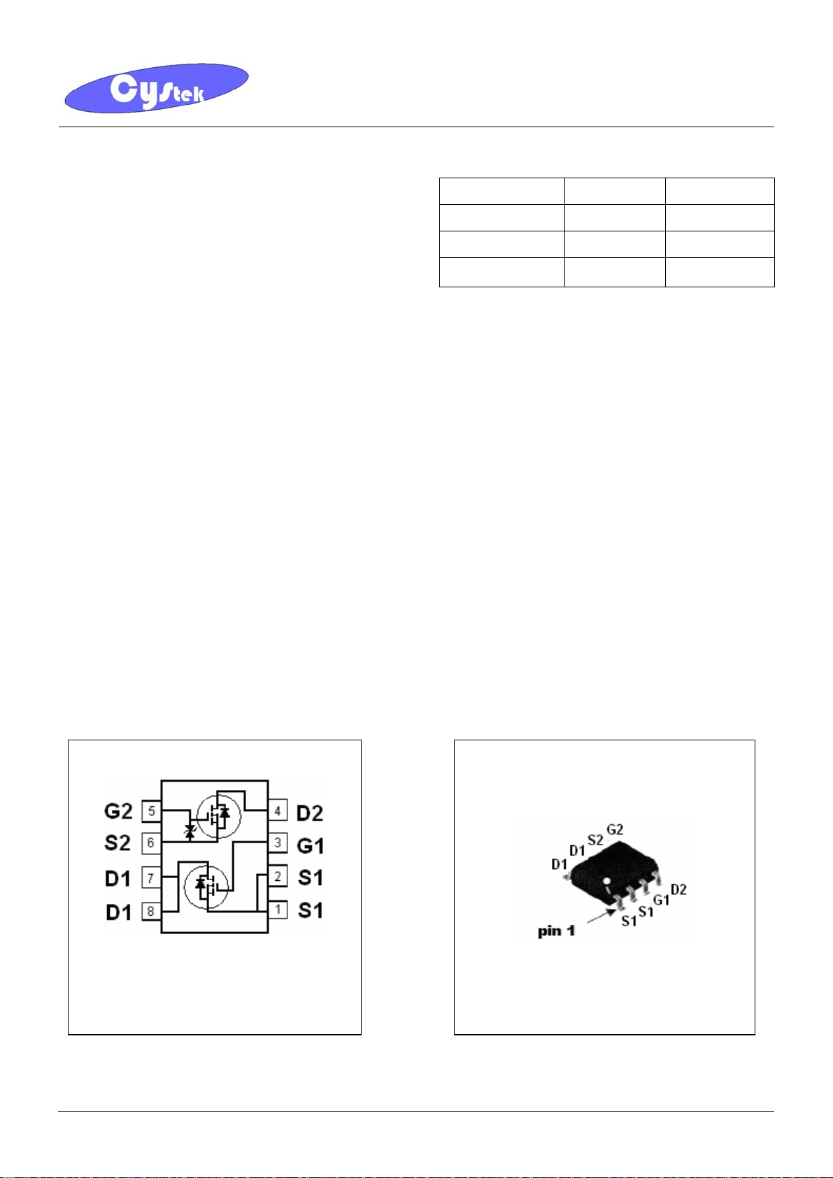
Equivalent Circuit Outline
MTNN20N03Q8 SOP-8
G:Gate
S:Source
D:Drain
MTNN20N03Q8 CYStek Product Specification
CYStech Electronics Corp.
Absolute Maximum Ratings (Ta=25°C)
Spec. No. : C805Q8
Issued Date : 2009.12.30
Revised Date :2011.03.21
Page No. : 2/9
Parameter Symbol
Unit
N-CH 1 N-CH 2
Drain-Source Voltage VDS 30 60 V
Limits
Gate-Source Voltage VGS
D 8 0.115 A
Continuous Drain Current @ TC=25 °C (Note 1)
Continuous Drain Current @ TC=100 °C (Note 1)
I
I
D 6 0.08 A
±20 ±20
V
Pulsed Drain Current (Note 2&3) IDM 32 0.7 A
Total Power Dissipation @ TA=25 °C
Linear Derating Factor
ESD susceptibility (Note 4)
Operating Junction Temperature Tj -55~+150
Storage Temperature Tstg -55~+150
Thermal Resistance, Junction-to-Ambient (Note 1) Rth,ja 62.5
Note : 1. Surface mounted on 1 in² copper pad of FR-4 board; 135°C/W when mounted on minimum copper pad.
2. Pulse width limited by maximum junction temperature.
3. Pulse width≤300μs, duty cycle≤2%.
4. Human body model, 1.5kΩ in series with 100pF
Pd 2 0.4 W
0.016 0.016
1250 V
W / °C
°C
°C
°C/W
Characteristics (Tj=25°C, unless otherwise specified)
N-Channel MOSFET 1
Symbol Min. Typ. Max. Unit Test Conditions
Static
BV
30 - - V VGS=0, ID=250μA
DSS
V
1.0 1.5 3.0 V VDS = VGS, ID=250μA
GS(th)
GFS - 16 - S VDS =5V, ID=8A
I
- -
GSS
- - 1 VDS =24V, VGS =0
- - 25
- 15.5 20 VGS =10V, ID=8A
- 23 31
*R
I
DSS
DS(ON)
±
100
nA
μA
mΩ
VGS=±20
V
=20V, VGS =0, Tj=125°C
DS
V
=5V, ID=6A
GS
Dynamic
*Qg(VGS=10V) - 11 -
*Qg(VGS=5V) - 6 -
*Qgs - 1.2 -
nC I
=8A, VDS=15V, VGS=10V
D
*Qgd - 3.3 -
*td
- 11 -
(ON)
V
=15V, ID=1A,VGS=10V,
R
DS
=6Ω
G
*tr - 16 -
*td
- 36 -
(OFF)
ns
*tf - 20 -
Ciss - 1115 -
Coss - 116 -
pF V
=0V, VDS=15V, f=1MHz
GS
Crss - 82 -
Ω
Rg - 2 -
VGS=15mV, VDS=0V, f=1MHz
MTNN20N03Q8 CYStek Product Specification
Spec. No. : C805Q8
CYStech Electronics Corp.
Issued Date : 2009.12.30
Revised Date :2011.03.21
Page No. : 3/9
Source-Drain Diode
*IS - - 2.3
*ISM - - 9.2
*VSD - - 1.2 V IF=I
*trr - 50 - ns
*Qrr - 2 - nC
A
S, VGS
, VGS=0, dI/dt=100A/μs
I
F=IS
=0V
N-Channel MOSFET 2
Symbol Min. Typ. Max. Unit Test Conditions
BV
V
R
60 - - V VGS=0, ID=10μA
DSS*
1 - 2.5 V VDS=VGS, ID=250μA
GS(th)
I
- - ±10 μA VGS=±20V, VDS=0
GSS
I
- - 1 μA VDS=60V, VGS=0
DSS
DS(ON)*
- 3.6 5.5 ID=100mA, VGS=5V
- 3 5
Ω
ID=100mA, VGS=10V
GFS 100 - - mS VDS=10V, ID=100mA
C
- 30.5 -
iss
C
- 9.3 -
oss
C
- 5.9 -
rss
pF VDS=10V, VGS=0, f=1MHz
*Pulse Test : Pulse Width ≤300μs, Duty Cycle≤2%
Ordering Information
Device Package Shipping
MTNN20N03Q8
(Pb-free lead plating package)
SOP-8
3000 pcs / Tape & Reel
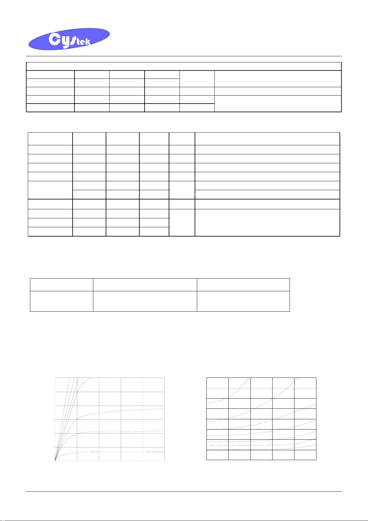
Typical Characteristics
N-CH MOSFET 1
30
V = 10 V
GS
25
20
15
10
D
I - Drain Current (A)
5
0
0
On-Region Charact eri sti cs
6V
7V
5V
12
V - Dr ain Source Voltage(V)
DS
4.5V
4V
3.5V
3
4
5
On-Resistance Vari ation wi th Drain Cur rent and Gat e Volt age
2.4
2.2
V = 3. 5 V
GS
2.0
1.8
1.6
1.4
DS(ON)
1.2
1.0
R -Normalized
Drain-Source On-Resist ance
0.8
0
4.0 V
4.5 V
6
12
I - Drain Curr ent (A)
D
5.0 V
6.0 V
7.0 V
18 24
10 V
30
MTNN20N03Q8 CYStek Product Specification
 Loading...