

CYStech MTNK1N3 Schematic [ru]
CYStech Electronics Corp.
N-CHANNEL MOSFET
MTNK1N3
Description
The MTNK1N3 is a N-channel enhancement-mode MOSFET.
Features
• Low on-resistance
• High ESD
• High speed switching
• Low-voltage drive(4V)
• Easily designed drive circuits
• Easy to use in parallel
• Pb-free package
Spec. No. : C320N3
Issued Date : 2007.11.06
Revised Date :2010.03.10
Page No. : 1/7
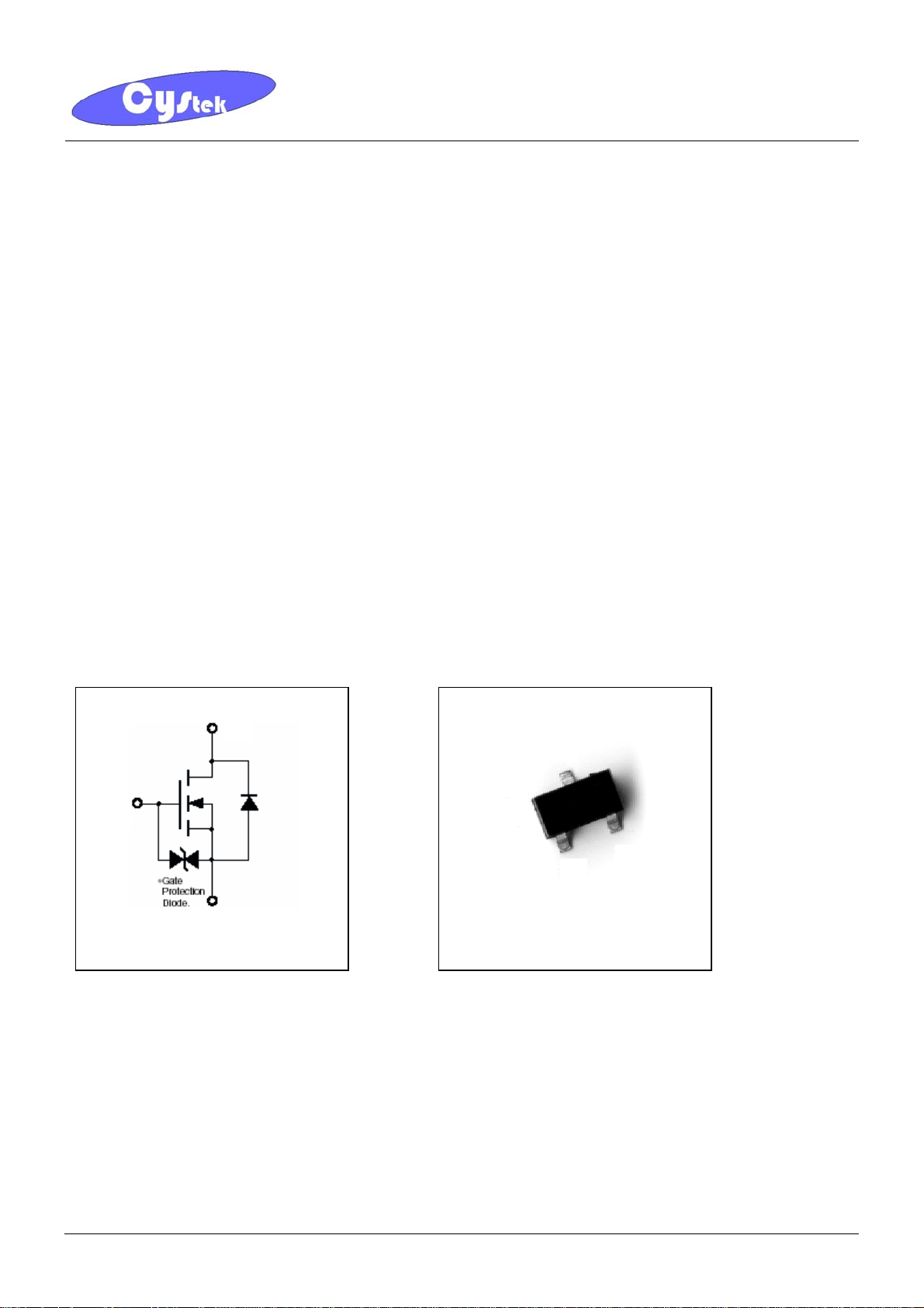
Symbol Outline
MTNK1N3 SOT-23
D
G
S
G:Gate
S:Source
D:Drain
D
S
G
MTNK1N3 CYStek Product Specification
Spec. No. : C320N3
CYStech Electronics Corp.
Issued Date : 2007.11.06
Revised Date :2010.03.10
Page No. : 2/7
Absolute Maximum Ratings (Ta=25°C)
Parameter Symbol Limits Unit
Drain-Source Voltage VDSS 60 V
Gate-Source Voltage
Drain Current
Drain Reverse Current
Continuous ID
Pulsed I
Continuous IDR
Pulsed IDRP
Total Power Dissipation
ESD susceptibility
Channel Temperature
Storage Temperature
Note : *1. Pulse Width ≤ 300μs, Duty cycle ≤2%
*2. When the device is mounted on a glass epoxy board with area measuring 1×0.75×0.62 inch
*3. Human body model, 1.5kΩ in series with 100pF
VGSS
DP
P
D
TCH
Tstg
±20 V
115 mA
700 *1 mA
115 mA
700 *1 mA
200 *2 mW
1250 *3 V
+150
-55~+150
°C
°C
Electrical Characteristics (Ta=25°C)
Symbol Min. Typ. Max. Unit Test Conditions
BV
V
R
60 - - V VGS=0, ID=10μA
DSS*
1 - 2.5 V VDS=VGS, ID=250μA
GS(th)
I
- - ±10 μA VGS=±20V, VDS=0
GSS
I
- - 1 μA VDS=60V, VGS=0
DSS
DS(ON)*
- 3.6 5.5 ID=100mA, VGS=5V
- 3 5
Ω
ID=100mA, VGS=10V
GFS 100 - - mS VDS=10V, ID=100mA
C
- 7.32 -
iss
C
- 3.42 -
oss
C
- 7.63 -
rss
pF VDS=10V, VGS=0, f=1MHz
td(on) - 1.2 -
=30V, ID=200mA, RGS=25Ω,
V
tr - 1 -
td(off) - 1.1 -
ns
DD
VGS=10V, RL=15Ω
tf - 2.2 -
*Pulse Test : Pulse Width ≤380μs, Duty Cycle≤2%
Ordering Information
Device Package Shipping Marking
MTNK1N3
SOT-23
(Pb-free)
3000 pcs / Tape & Reel 702
MTNK1N3 CYStek Product Specification
CYStech Electronics Corp.
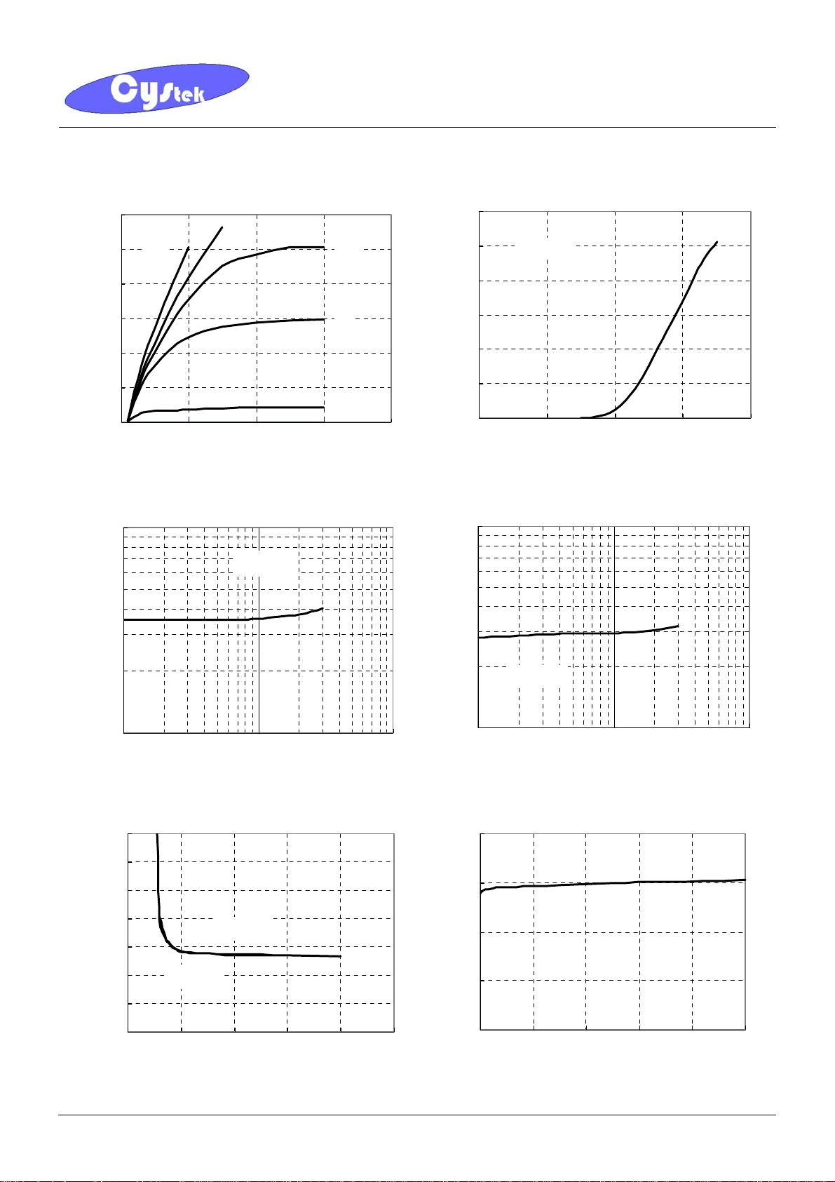
Characteristic Curves
Spec. No. : C320N3
Issued Date : 2007.11.06
Revised Date :2010.03.10
Page No. : 3/7
Typical Output Characteristics
0.3
0.25
0.2
0.15
0.1
Drain Current - ID(A)
0.05
6V
0
01234
4V
3.5V
3V
VGS= 2. 2V
Drain-Source Voltage -VDS(V)
0.3
0.25
0.2
0.15
0.1
Drain Current -ID(A)
0.05
0
01234
Typical Transfer Characteristics
VDS= 10V
Gate-Source Voltage-VGS(V)
Static Drain-Source On-State resistance vs Drain Current
10
VGS=5V
St ati c Dra in-Sourc e On-Sta te re si stanc e vs Drain Curre nt
10
Resistance-RDS(o n)(Ω)
Static Drain-Source On-State
1
0.01 0.1 1
Drain Current-ID(A)
Static Drain-Source On-State Resistance vs Gate-Source
Voltage
7
6
5
4
3
2
Resistance-RDS(ON)(Ω)
Static Drain-Source On-State
1
0
ID=50mA
0 5 10 15 20 25
ID=100mA
Gate-Source Voltage-VGS(V)
Resistance-RDS(on)(Ω)
Static Drain-Source On-State
1
0.01 0.1 1
10
1
0.1
0.01
Source-Drain Voltage-VSD(V)
0.001
VGS= 10V
Drain Current-ID(A)
Reverse Drain Current vs Source-Drain Voltage
0 0.2 0.4 0.6 0.8 1
Reverse Drain Current -IDR(A)
MTNK1N3 CYStek Product Specification
 Loading...