

CYStech MTN2302N3 Schematic [ru]
CYStech Electronics Corp.
20V N-CHANNEL Enhancement Mode MOSFET
MTN2302N3
Features
VDS=20V
•
R
R
Advanced trench process technology
•
High density cell design for ultra low on resistance
•
Excellent thermal and electrical capabilities
•
Compact and low profile SOT-23 package
•
=65mΩ@VGS=4.5V, IDS=3.6A
DS(ON)
=95mΩ@VGS=2.5V, IDS=3.1A
DS(ON)
Spec. No. : C323N3
Issued Date : 2004.04.05
Revised Date : 2004.10.22 . .
Page No. : 1/5
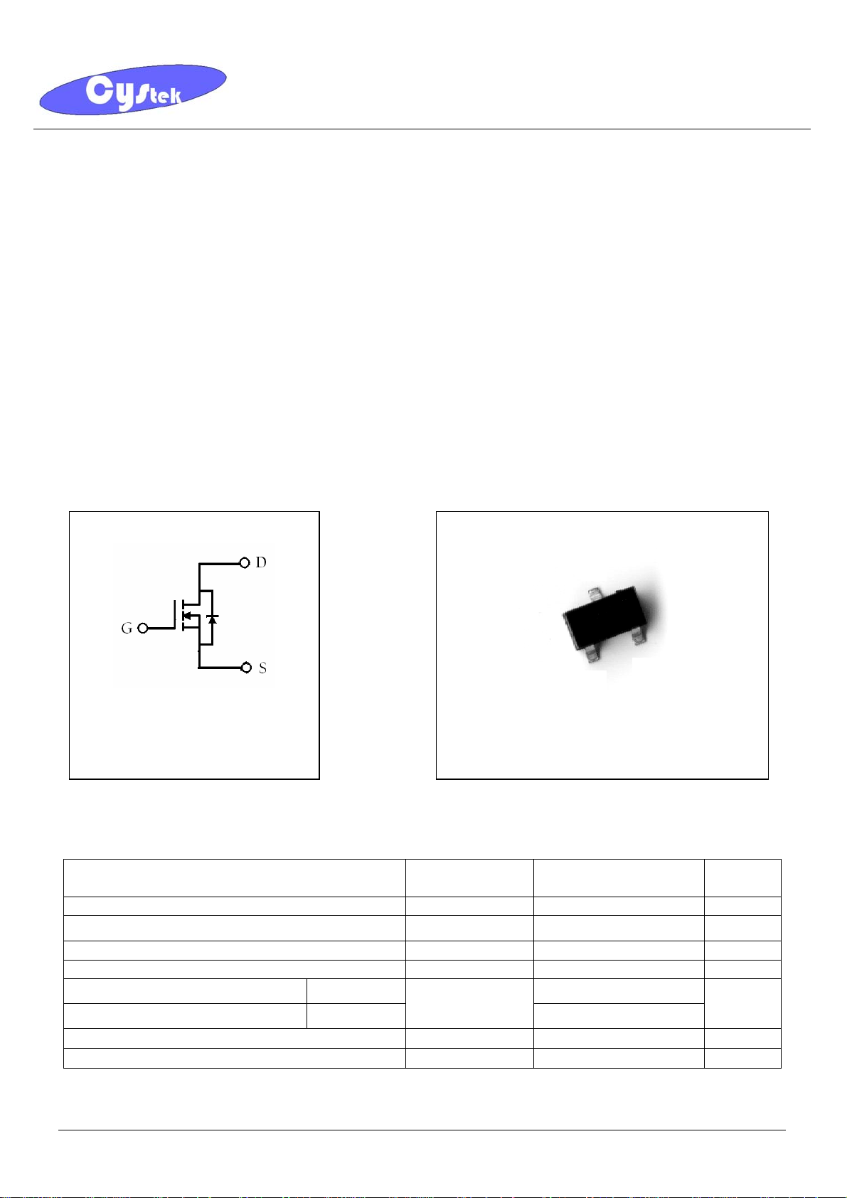
Equivalent Circuit Outline
MTN2302N3
G:Gate
S:Source
D:Drain
Absolute Maximum Ratings (Ta=25°C)
Parameter Symbol Limits Unit
SOT-23
D
S
G
Drain-Source Voltage VDS 20 V
Gate-Source Voltage VGS ±8 V
Continuous Drain Current ID 2.4 A
Pulsed Drain Current IDM 10 A
Maximum Power Dissipation
Operating Junction Temperature Tj -55~+150
Storage Temperature Tstg -55~+150
MTN2302N3 CYStek Product Specification
Ta=25℃
Ta=75℃
P
D
1.25
W
0.8
°C
°C
Thermal Performance
Parameter Symbol Limit Unit
CYStech Electronics Corp.
Spec. No. : C323N3
Issued Date : 2004.04.05
Revised Date : 2004.10.22 . .
Page No. : 2/5
Thermal Resistance, Junction-to-Ambient(PCB mounted) Rth,ja 100
Lead Temperature, for 5 second Soldering(1/8” from case) TL 260
Note : Surface mounted on FR-4 board, t≦5sec.
Electrical Characteristics (Ta=25°C)
Symbol Min. Typ. Max. Unit Test Conditions
Static
BV
V
*I
20 - - V VGS=0, ID=250µA
DSS
0.45 - - V VDS=VGS, ID=250µA
GS(th)
I
- - 100 nA VGS=+8V, VDS=0
GSS/F
I
- - -100 nA VGS=-8V, VDS=0
GSS/R
I
- - 1 µA VDS=20V, VGS=0
DSS
6 - - A VDS=5V, VGS=4.5V
D(ON)
- 50 65 ID=3.6A, VGS=4.5V
*R
DS(ON)
- 75 95
mΩ
ID=3.1A, VGS=2.5V
*GFS - 10 - S VDS=5V, ID=3.6A
Dynamic
Ciss - 450 -
Coss - 70 -
pF VDS=10V, VGS=0, f=1MHz
Crss - 43 -
t
- 7 15
d(ON)
V
=10V, ID=1A, RL=10Ω
tr - 55 80
t
- 16 60
d(OFF)
ns
DD
V
=4.5V, RG=6Ω
GEN
tf - 10 25
Qg - 5.2 10
Qgs - 0.65 -
nC
Qgd - 1.5 -
VDS=10V, ID=3.6A,
V
=4.5V,
GS
Source-Drain Diode
ISD - - 1.6 A -
VSD - 0.75 1.2 V VGS=0V, ISD=1A
*Pulse Test : Pulse Width ≤300µs, Duty Cycle≤2%
°C/W
°C
MTN2302N3 CYStek Product Specification
 Loading...