

CYStech MTA90N03ZN3 Schematic [ru]
CYStech Electronics Corp.
30V N-Channel Enhancement Mode MOSFET
MTA90N03ZN3
Features
Simple drive requirement.
•
Small package outline.
•
ESD protected.
•
Pb-free lead plating and halogen-free package.
•
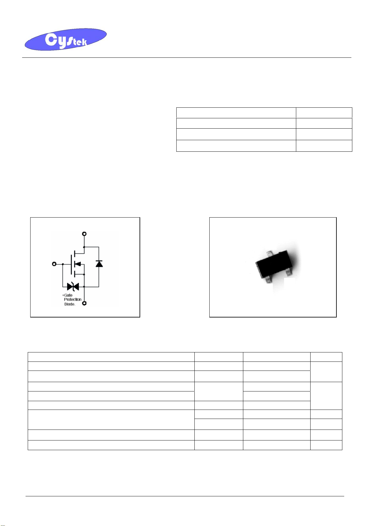
Symbol Outline
BVDSS 30V
ID
RDSON@VGS=4.5V, ID=2.5A
RDSON@VGS=3V,ID=2.5A
Spec. No. : C831N3
Issued Date : 2012.07.04
Revised Date : 2012.12.28
Page No. : 1/8
3.2A
130mΩ(typ)
144mΩ(typ)
MTA90N03ZN3 SOT-23
D
G:Gate
S:Source
D:Drain
G
S
Absolute Maximum Ratings (Ta=25°C)
Parameter
Drain-Source Voltage VDS 30
Gate-Source Voltage VGS ±12
Continuous Drain Current @ TA=25°C , VGS=4.5V
Continuous Drain Current @ TA=70°C, VGS=4.5V
Pulsed Drain Current (Notes 1, 2) IDM 10
Maximum Power Dissipation@ TA=25℃
Linear Derating Factor
ESD susceptibility
Operating Junction and Storage Temperature Tj, Tstg -55~+150
Note : 1. Pulse width limited by maximum junction temperature.
2. Pulse width≤ 300μs, duty cycle≤2%.
3. Surface mounted on 1 in² copper pad of FR-4 board, t≤10s.
4. Human body model, 1.5kΩ in series with 100pF.
Symbol Limits Unit
ID
PD 1.38 (Note 3) W
0.01
1000 (Note 4) V
3.2
2.6
V
A
W/°C
°C
MTA90N03ZN3 CYStek Product Specification
Thermal Performance
Parameter Symbol Limit Unit
CYStech Electronics Corp.
Spec. No. : C831N3
Issued Date : 2012.07.04
Revised Date : 2012.12.28
Page No. : 2/8
Thermal Resistance, Junction-to-Ambient(PCB mounted) Rth,ja 90
Note : Surface mounted on 1 in² copper pad of FR-4 board, 270°C/W when mounted on minimum copper pad.
Electrical Characteristics (Tj=25°C, unless otherwise noted)
Symbol Min. Typ. Max. Unit Test Conditions
Static
BV
V
30 - - V VGS=0, ID=250μA
DSS
0.5 0.9 1.5 V VDS=VGS, ID=250μA
GS(th)
±
I
- -
GSS
I
DSS
- - 1 VDS=30V, VGS=0
- - 10
10 VGS=±12V, VDS=0
μA
VDS=24V, VGS=0 (Tj=70
- 130 160 VGS=4.5V, ID=2.5A
*R
DS(ON)
- 145 180
mΩ
VGS=3V, ID=2.5A
*GFS - 5.4 - S VDS=3V, ID=1.6A
Dynamic
Ciss - 309 -
Coss - 50 -
pF VDS=10V, VGS=0, f=1MHz
Crss - 38 -
t
- 15 -
d(ON)
tr - 35 -
t
- 51 -
d(OFF)
ns
VDS=15V, ID=500mA, VGS=2.5V,
RG=6Ω
tf - 27 -
Qg - 8 -
Qgs - 0.8 -
nC VDS=15V, ID=3.2A, VGS=4.5V
Qgd - 2.8 -
Source-Drain Diode
*VSD - 0.8 1.2 V VGS=0V, IS=1A
*Pulse Test : Pulse Width ≤300μs, Duty Cycle≤2%
°C)
°C/W
Ordering Information
Device Package Shipping
MTA90N03ZN3-0-T1-G
(Pb-free lead plating and halogen-free package)
SOT-23
3000 pcs / Tape & Reel
MTA90N03ZN3 CYStek Product Specification
GS
V
GS
Typical Characteristics
CYStech Electronics Corp.
Spec. No. : C831N3
Issued Date : 2012.07.04
Revised Date : 2012.12.28
Page No. : 3/8
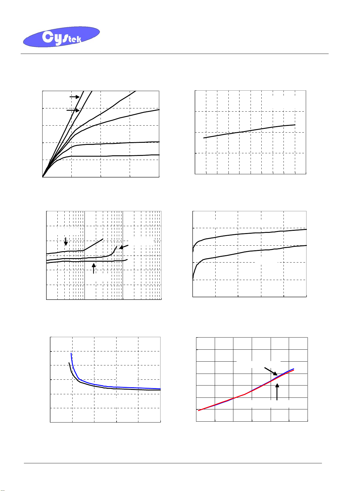
Typical Output Characteristics
10
V
=10V
GS
8
VGS=4.5V
6
4
, Drain Current (A)
D
I
2
0
00.511.5
Static Drain-Source On-State resistance vs Drain Current
300
250
200
150
Resistance(mΩ)
100
, Static Drain-Source On-State
DS (on)
50
R
VGS=2V
, Drain-Source Voltage(V)
V
DS
VGS=4.5V
VGS=3V
V =2.5V
VGS=2V
VGS=1.8
VGS=3V
Breakdown Voltage
, Normalized Drain-Source
DSS
BV
2
, Source-Drain Voltage(V)
SD
V
Brekdown Voltage vs Ambient Temperature
1.4
ID=250μA,
V
=0V
1.2
1
0.8
0.6
-75 -50 -25 0 25 50 75 100 125 150 175
Tj, Junction Temperature(°C)
Reverse Drain Current vs Source-Drain Voltage
1
VGS=0V
Tj=25°C
0.8
0.6
0.4
Tj=150°C
0.2
0
0.1 1 10 100
D
, Drain Current(A)
I
Static Drain-Source On-State Resistance vs Gate-Source
Voltage
300
250
200
150
ID=2.5A
0
0 0.2 0.4 0.6 0.8 1
, Reverse Drain Current (A)
I
DR
Drain-Source On-State Resistance vs Junction Tempearture
2
1.8
1.6
VGS=3V, ID=2.5A
1.4
1.2
, Static Drain-Source On-
100
State Resistance(mΩ)
DS(ON)
50
R
ID=100mA
0
024681
V
, Gate-Source Voltage(V)
GS
, Normalized Static Drain-
DS( ON)
R
0
1
Source On-State Resistance
VGS=4.5V, ID=2.5A
0.8
0.6
-60 -20 20 60 100 140 180
Tj, Junction Temperature(°C)
MTA90N03ZN3 CYStek Product Specification
 Loading...