

CYRTK ES51988 Datasheet
ES51988
3 3/4 AUTO REL/MAX/MIN
Features:
•Full Automatic measurement
•3 3/4 digits display
•Frequency measurement (40M HZ)
•Rotary or push setting mode
•Auto-power-off then hold the final data
•Rotary or push re-power on function
•Data hold, MAX/MIN hold, Relative
data when this function is pressed
•Low battery detect (3V & 9V)
•On chip buzzer driver
•3V DC power supply
•Internal AC to DC conversion OP AMP
If non_AC mode , OP will become unit
gain buffer.
•Serial Data Output (RS232 format)
•LCD segment check
•100 Pin flat-package
Description:
The ES51988 is an integrated analogto-digital converter (ADC)with 3 3/4 digits
and 42-segment bargraph LCD display,
automatic range, and 3V battery power
supply.
Automatic range selection is provided
for voltage (AC/DC) measurement, ohm
measurement, current(uA and mA)
measurement,and frequency counter. The
ES51988 also provides serial data output
function.
Expensive and bulky mechanical range
switches are not required. The other
functions are provided for MAX and MIN
holding and current value display, data
holding, Relative data and reference value
display, low battery detection, auto-poweroff, diode measurement, continuity
checking.
Absolute Maximum Ratings
Characteristics Ratings
Supply Voltage (V- to AGND) -4V
Analog Input Voltage V+ to VDigital Input V- to DGND
Power Dissipation Flat Package 500mW
Operating Temperature
Storage Temperature
0℃ to 70℃
-25℃ to 125℃
1 91年11月28日
ES51988
3 3/4 AUTO REL/MAX/MIN
Electrical Characteristics
TA=25℃,V- = -3V
Symbol Parameter Test Condition Min. Typ. Max. Count
V- Power Supply -3.5 -3.0 -2.2 Volt
Idd
Iss
REV
REB
NLV
NLB
VREF
Operating Supply Current Normal Power On
Auto-power-off
Rollover Error
(Voltage)
Rollover Error
(Bargraph)
Nonlinearity
(Voltage)
Nonlinearity
(Bargraph)
Input Leakage - 1 10 pA
Low Battery Flag Voltage V- to AGND -2.5 -2.3 -2.1 V
Zero Input Reading
Reference Voltage and 400Ω
measurement
Peak to Peak Backplane Drive
Voltage
Counter Time Base Period fosc=4MHz - 1 - Sec
Open Circuit Voltage for Ω
Measurement(except 400Ω)
Pull High to 0V Resistance FC1,FC2,FC3,FC4
Pull High to 0V Resistance KEY, SET - 250 AC Frequency Response
(4V range)
10M input
Resistor
Best Case
Straight Line
10MΩInput Resistor
100KΩ Between
VRH and AGND
-3.2≦V-≦-2.2
Ω and Continuity
Function
FC5,RANGE,HOLD,
MAX/MIN,REL
± 0.5﹪Error
± 2.5﹪Error
-
1.0
-
0.1
-
-
-
-
-000 000 +000 Count
-1.3 -1.2 -1.1 V
2.85 3.0 3.15 V
-0.5 -0.45 -0.4 V
- 2.5 -
--40 to
500
40 to
2000
-
-
-
-
1.55mA
± 0.1
± 0.5
± 0.1
± 0.5
﹪F.S.
﹪F.S.
﹪F.S.
﹪F.S.
-
-
uA
MΩ
KΩ
HZ
TCRF Reference Voltage
Temperature Coefficient
2 91年11月28日
100KΩBetween VRH
and AGND
0℃<TA<70℃
-50-
ppm/℃
ES51988
3 3/4 AUTO REL/MAX/MIN
Pin Description
Pin No. Symbol Description
1 V+ Positive supply voltage,output of on-chip DC-DC converter.
2 V+ Positive supply voltage,output of on-chip DC-DC converter.
3 CH+ High speed positive connection for reference capacitor.
4 CH- High speed negative connection for reference capacitor.
5 CIH High speed integrator output. Connected to integration capacitor.
6 BUFH Integration resistor connection for high speed buffer output.
7 CAZH High speed auto-zero capacitor connection
8 CL+ High resolution positive connection for reference capacitor.
9 CL- High resolution negative connection for reference capacitor.
10 CIL High resolution integrator output. Connected to integration capacitor.
11 CAZL High resolution auto-zero capacitor connection.
12 BUFL Integration resistor connection for high resolution buffer output.
13 IVSH High level current measurement input.
14 IVSL Low level current measurement input
15 OVX Input high voltage for resistance measurement.
16 OVH Output connection for resistance measurement.
17 OVSG Sense low voltage for resistance measurement.
18 OR1
19 VR5
20 VR4
21 VR3
22 VR2
23 TEST5 Test pin 5.
24 ACVL Negative output of AC to DC converter.
25 ACVH Positive output of AC to DC converter.
26 ADI Negative input of internal AC to DC OP AMP.
27 ADO Output of internal AC to DC OP AMP.
28 NC
29 NC
30 NC
31 SGND Signal ground.
32 VR1 Unknown voltage input .
33 NC
34 VR Reference input voltage connection. Typically -100 mV.
35 VRH Output of band-gap voltage reference. Typically -1.2 V.
36 ACVR Optional pin. When connected to -3V,ACV without 400mV range.
37 NC
Reference resistor connection for 399.9Ωrange.
Voltage measurement ÷ 10000 attenuator (3999V).
Voltage measurement ÷ 1000 attenuator (399.9V).
Voltage measurement ÷ 100 attenuator (39.99V).
Voltage measurement ÷ 10 attenuator (3.999V).
3 91年11月28日
ES51988
3 3/4 AUTO REL/MAX/MIN
Pin. No Symbol. Description
38 SLEEP When auto-power-off happen, this pin output will change from +3V
to –3V. When re-power on happens, this pin output will change back to
+3V.
39 TEST1 Test pin 1.
40 NC
41 FREQ Frequency counter input, offset to 1/2(V-).
42 SET Input to set serial data output. Pulse low to make this function active.
43 F100 100 HZ square wave output.
44 SEG24 LCD Segment line 24.
45 SEG23 LCD Segment line 23.
46 SEG22 LCD Segment line 22.
47 SEG21 LCD Segment line 21
48 SEG20 LCD Segment line 20.
49 SEG19 LCD Segment line 19.
50 SEG18 LCD Segment line 18.
51 SEG17 LCD Segment line 17.
52 SEG16 LCD Segment line 16.
53 SEG15 LCD Segment line 15.
54 SEG14 LCD Segment line 14.
55 SEG13 LCD Segment line 13.
56 SEG12 LCD Segment line 12.
57 SEG11 LCD Segment line 11.
58 SEG10 LCD Segment line 10.
59 SEG9 LCD Segment line 9.
60 SEG8 LCD Segment line 8.
61 SEG7 LCD Segment line 7.
62 SEG6 LCD Segment line 6.
63 SEG5 LCD Segment line 5.
64 SEG4 LCD Segment line 4.
65 SEG3 LCD Segment line 3.
66 SEG2 LCD Segment line 2.
67 SEG1 LCD Segment line 1.
68 ANNUNC Square-wave output at the backplane frequency, synchronized to BP1.
ANNUNC can be used to control display annunciator. Connecting an
LCD segment to ANNUNC and turns it on; connecting an LCD
segment to its backplane and turns it off.
69 BP4 LCD Backplane 4.
70 BP3 LCD Backplane 3.
71 BP2 LCD Backplane 2.
72 BP1 LCD Backplane 1.
4 91年11月28日
ES51988
3 3/4 AUTO REL/MAX/MIN
Pin. No Symbol. Description.
73 NC
74 BUZOUT Buzzer output. Audio frequency (2.0KHz) output which drives a
piezoelectric buzzer.
75 NC
76 NC
77 NC
78 NC
79 OSC1 Crystal oscillator (input) connection.
80 OSC2 Crystal oscillator (output) connection.
81 NC
82 KEY Mode change pin.
83 REL Input to get relative display. Pulse low to make this function active.
84 MAX/MIN Input to set MAX/MIN display. Pulse low to make this function active.
85 HOLD Input to hold display. Pulse low to make this function active.
86 RANGE Input to set automatic/manual mode and manual range selection. Pulse
low to make this function active.
87 FC5 Switch 5 for function selection.
88 FC4 Switch 4 for function selection.
89 FC3 Switch 3 for function selection.
90 FC2 Switch 2 for function selection.
91 FC1 Switch 1 for function selection.
92 LBAT9 Low battery voltage setting. If used 3V battery, connected this pin to
AGND, the default low battery voltage will be –2.3V. If used 9V
battery, when the input voltage is small than VRH(-1.2V), the low
battery annunciator will be display.
93 SDO Serial data output.
94 C+ Positive capacitor connection for on-chip DC-DC converter.
95 C- Negative capacitor connection for on-chip DC-DC converter.
96 V- Negative supply voltage.Connecting to battery negative terminal.
97 V- Negative supply voltage.Connecting to battery negative terminal.
98 DGND Digital ground,connected to battery positive terminal.
99 AGND Analog ground.
100 AGND Analog ground.
5 91年11月28日
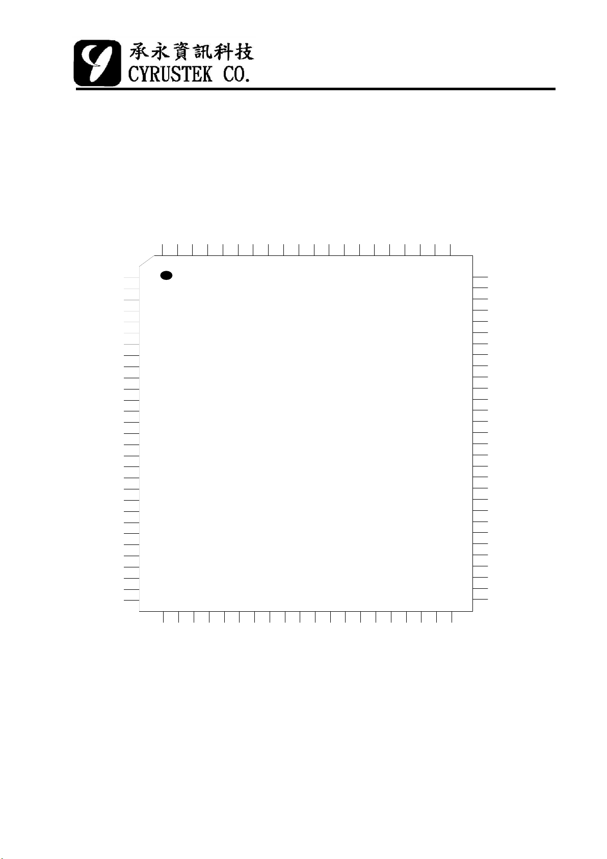
Pin Configuration
A
D
A
G
G
G
N
N
N
D
D
D
ES51988
3 3/4 AUTO REL/MAX/MIN
M
L
B
A
S
F
F
T
D
C
V
V
-
C
C
-
O
+
-
C
9
1
2
F
F
F
C
C
C
3
4
5
A
R
X
A
H
/
N
O
G
L
E
D
K
M
R
E
I
E
N
Y
N
L
C
CH+
CHCIH
BUFH
CAZH
CL+
CL-
CIL
CZAL
BUFL
IVSH
IVSL
OVX
OVH
OVSG
OR1
VR5
VR4
VR3
VR2
TEST5
ACVL
ACVH
ADI
ADO
NC
V+
V+
NC
NC
5
10
15
20
25
30
100
35
95
90
40 45
85
50
55
75
60
80
65
70
OSC2
OSC1
NC
NC
NC
NC
BUZOUT
NC
BP1
BP2
BP3
BP4
ANNUNC
SEG1
SEG2
SEG3
SEG4
SEG5
SEG6
SEG7
SEG8
SEG9
SEG10
SEG11
SEG12
SEG13
SEG14
SEG15
SEG16
SEG17
S
N
V
G
C
R
N
1
D
VRV
A
C
R
V
H
R
S
N
C
L
E
E
P
F
T
N
R
E
C
E
S
Q
T
1
S
S
F
E
1
E
G
0
T
2
0
4
S
S
S
E
E
E
G
G
G
2
2
2
1
2
3
S
S
S
E
E
E
G
G
G
1
1
2
8
9
0
6 91年11月28日
ES51988
3 3/4 AUTO REL/MAX/MIN
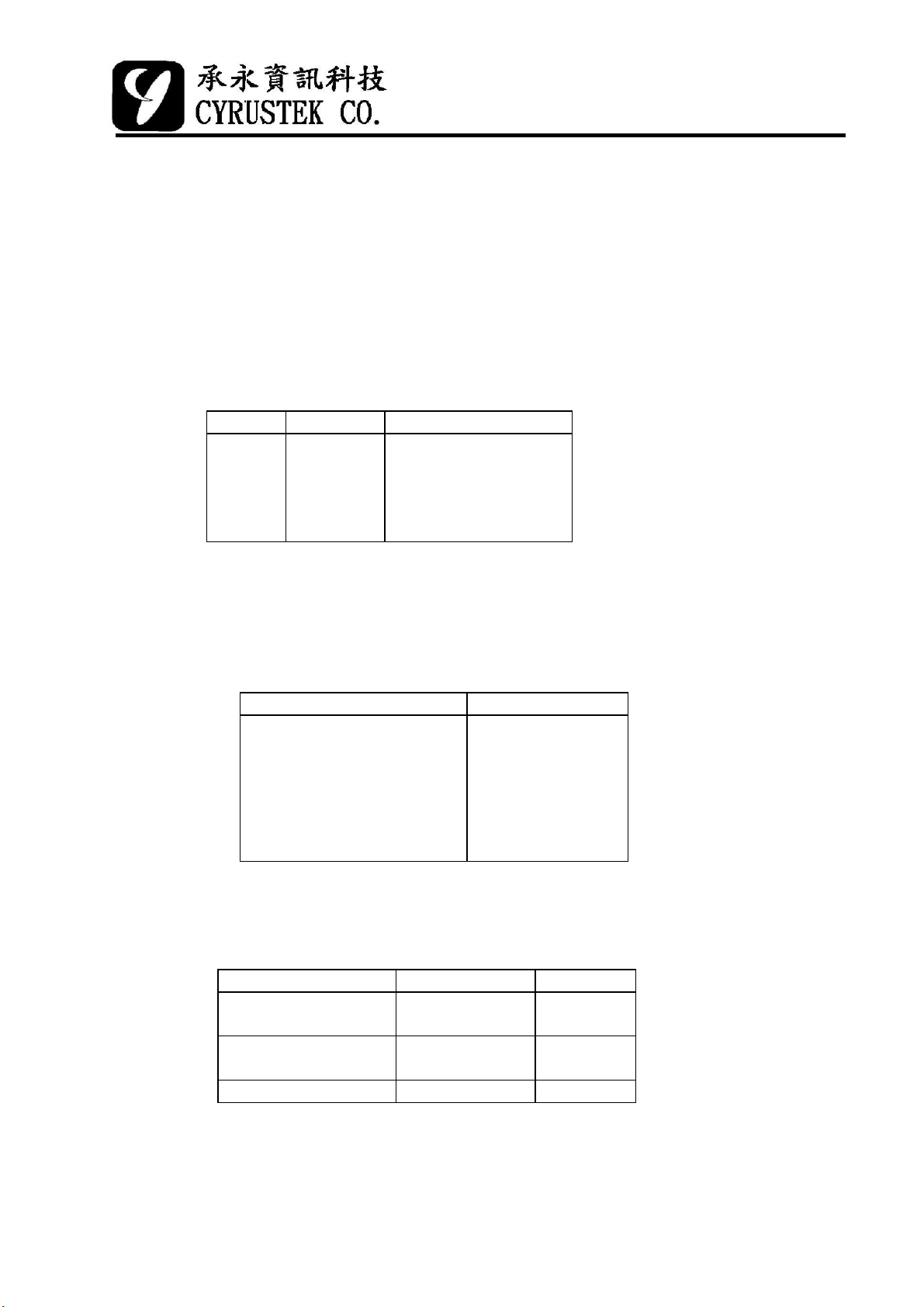
Operation Mode
(1) Measurement Description
Voltage Measurement
Resistive divider is automatically changed to provide in range reading
for 399.9mV to 3999V full scale reading. The following table shows
the various full scale range.
Range Full scale Resistive Ratio
VR1
VR2
VR3
VR4
VR5
399.9 mV
3.999 V
39.99 V
399.9 V
3999 V
1 , 1/1
R2/(R1+R2) , 1/10
R3/(R1+R3) , 1/100
R4/(R1+R4) , 1/1000
R5/(R1+R5) , 1/10000
Resistance Measurement
Resistive divider is automatically changed to provide the proper range.
The following table shows the various full scale range.
Range Full Scale Reference Resistor
OR1 399.9 Ω
OR2 3.999 KΩ
OR3 39.99 KΩ
OR4 399.9 KΩ
OR5 3.999 MΩ
OR6 39.99 MΩ
Current Measurement
In the current measurement mode , there are three range selections :
Mode Range Selection Full Scale
Automatic Mode 1 uA 399.9 uA
Automatic Mode 2 mA 39.99 mA
Manual Mode A 39.99 A
When the mode changes among (uA, mA, A), the original AC/DC
state will keep.
R6(100Ω)
R5(1KΩ)
R4(10KΩ)
R1||R3(=100KΩ)
R1||R2(=1MΩ)
R1(10MΩ)
3999 uA
399.9 mA
7 91年11月28日
 Loading...