

Page 1

Data Book
Cyrix Corporation Confidential
October 29, 1998 - Revision 2.0
Addenda and other updates for this manual can be obtained from
Cyrix Web site: www.cyrix.com.
Page 2

©1998 Copyright Cyrix Corporation. All rights reserved.
Printed in the United States of America
Cyrix is a registered trademark of Cyrix Corporation.
Cyrix Trademarks include: Cx5520, Display Compression Technology (DCT), MediaGX, XpressAUDIO,
XpressGRAPHICS, XpressRAM, Virtual System Architecture (VSA)
All other products mentioned herein are trademarks of their respective owners and are hereby recognized as such.
Cyrix is a wholly-owned subsidiary of National Semiconductor® Corp.
Cyrix Corporation
2703 North Central Expr essway
Richardson, Texas 75080
United States of America
Cyrix Corporation (Cyrix) reserves the right to make changes in the devices or specification described herein without
notice. Before design-in or order placement, customers are advised to verify that the information on which orders or
design activities are based is current. Cyrix warrants its products to conform to current specifications in accordance
with Cyrix’ standard warranty. Testing is performed to the extent necessary as determined by Cyrix to support this
warranty. Unless expl icitly specified by customer order r equirements, and agreed to in writing by Cyrix , not all device
characteristics are ne cess arily tested . Cyrix assu mes n o liab ility, unless specifically agreed to in wr itin g, for c ustom er’s
product design or infringement of patents or copyrights of third parties arising from use of Cyrix devices. No license,
either express o r implied, to Cyrix p aten ts, copyrights, or other intellectual p rope rty rights pertainin g to a ny m ac hin e o r
combination of Cyrix devices is hereby granted. Cyrix products are not intended for use in any medical, life saving, or
life sustaining systems. Information in this document is subject to change without notice.
ii Cyrix Corporation Confidential GXm_db_v2.0
Page 3
MediaGX™ MMX™-Enhanced Processor
Integrated x86 Solution with MMX Support
Introduction
♦
High Performance
- Processor speeds up to 300MHz
- Write-Back cache
- Memory management with Load Store and
Memory-Read Bypassing
- Six-stage integer pipeline
- XpressRAM™ and XpressGRAPHICS™
♦
MediaGX™ MMX™-Enhanced Processor
- Processor Integrated Functions:
- Graphics Pipeline
- Memory Controller (SDRAM)
- Display Controller
- PCI Controller
- Interfaces with Cx5520 or Cx5530 I/O
Companion chip
- 320 SPGA or 352 BGA package
♦
x86 Instruction Set with MMX Support
- Compatible with MMX Technology
- Runs Windows
NT, DOS, UNIX
®
95, Windows 3.x, Windows
®
, OS/2®, Solaris®, and others
The MediaGX™ MMX™-Enhanced Processor, in
combination with the Cx5520 or Cx5530 I/O
Companion chip provides advanced video and
audio functions and permits direct interface to
memory. This high-performance 64-bit processor is
x86 instruction set compatible and supports MMX
technology.
This processor is the latest member of the Cyrix
MediaGX family, offering high performance, fully
accelerated 2D graphics, a synchronous memory
interface and a PCI bus controller, all on a single
chip. As described in separate manuals, the
Cx5520 and Cx5530 I/O Companion chips enable
the full fe atures of the MediaGX processor with
MMX support. These features include full VGA and
VESA video, 16-bit stereo sound, IDE interface,
ISA interface, SMM power management, and AT
compatibility logic. In addition, the newer Cx5530
provides an Ultra DMA/33 interface, MPEG2
assist, and is AC97 Version 2.0 compliant audio.
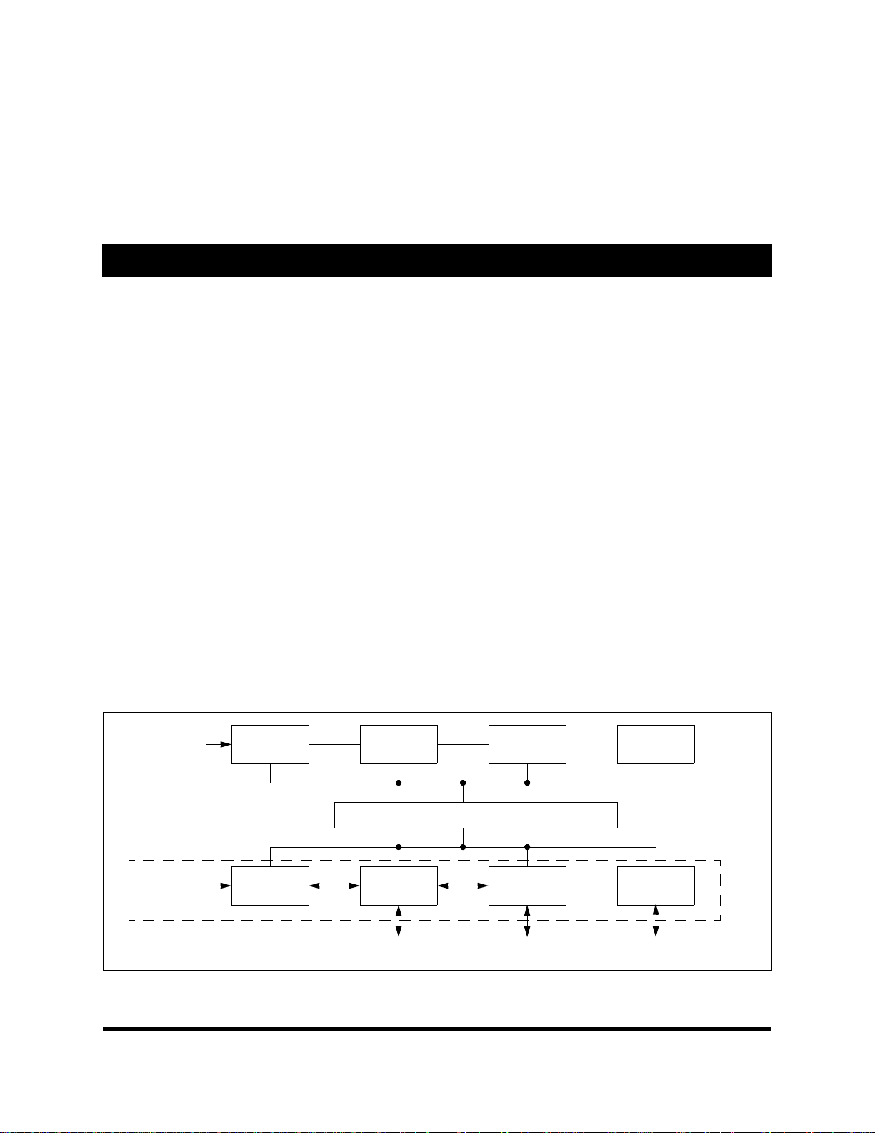
Write-Back Floating
Cache Unit Mgmt Unit Unit Point Unit
C-Bus
X-Bus
Integrated
Functions
GXm_db_v2.0 Cyrix Corporation Confidential Page iii
Graphics Memory Display PCI
Pipeline ControllerControllerController
Memory
Internal Bus Interface Unit
SDRAM Port Cx5520/Cx5530 PCI Bus
Internal Block Diagram
Integer
(CRT/LCD TFT)
Page 4

Page iv Cyrix Corporation Confidential GXm_db_v2.0
Page 5

MediaGX™ MMX™-Enhanced Processor
Integrated x86 Solution with MMX Support
Table of Contents
Table of Contents
1 Overview . . . . . . . . . . . . . . . . . . . . . . . . . . . . . . . . . . . . . . . . . . . . . .1
1.1 Architecture . . . . . . . . . . . . . . . . . . . . . . . . . . . . . . . . . . . . . . . . . .3
1.1.1 Integer Unit . . . . . . . . . . . . . . . . . . . . . . . . . . . . . . . . . . . . . .4
1.1.2 Floating Point Unit . . . . . . . . . . . . . . . . . . . . . . . . . . . . . . . . . . .4
1.1.3 Write-Back Cache Unit . . . . . . . . . . . . . . . . . . . . . . . . . . . . . . . . .4
1.1.4 Memory Management Unit . . . . . . . . . . . . . . . . . . . . . . . . . . . . . . .5
1.1.5 Internal Bus Interface Unit . . . . . . . . . . . . . . . . . . . . . . . . . . . . . . .5
1.2 Integrated Functions . . . . . . . . . . . . . . . . . . . . . . . . . . . . . . . . . . . . .5
1.2.1 Graphics Accelerator . . . . . . . . . . . . . . . . . . . . . . . . . . . . . . . . .5
1.2.2 Display Controller . . . . . . . . . . . . . . . . . . . . . . . . . . . . . . . . . . .6
1.2.3 XpressRAM™ Memory Subsystem . . . . . . . . . . . . . . . . . . . . . . . . . .6
1.2.4 PCI Controller . . . . . . . . . . . . . . . . . . . . . . . . . . . . . . . . . . . . .6
1.3 System Designs . . . . . . . . . . . . . . . . . . . . . . . . . . . . . . . . . . . . . . .7
2 Signal Definitions . . . . . . . . . . . . . . . . . . . . . . . . . . . . . . . . . . . . . . . . .9
2.1 Pin Assignments . . . . . . . . . . . . . . . . . . . . . . . . . . . . . . . . . . . . . . 10
2.2 Signal Descriptions . . . . . . . . . . . . . . . . . . . . . . . . . . . . . . . . . . . . . 21
2.2.1 System Interface Signals . . . . . . . . . . . . . . . . . . . . . . . . . . . . . . 21
2.2.2 PCI Interface Signals . . . . . . . . . . . . . . . . . . . . . . . . . . . . . . . . 24
2.2.3 Memory Controller Interface Signals . . . . . . . . . . . . . . . . . . . . . . . . 28
2.2.4 Video Interface Signals . . . . . . . . . . . . . . . . . . . . . . . . . . . . . . . 30
2.2.5 Power, Ground, and No Connect Signals . . . . . . . . . . . . . . . . . . . . . 32
2.2.6 Cyrix Internal Test and Measurement Signals . . . . . . . . . . . . . . . . . . . . 33
2.3 Subsystem Signal Connections . . . . . . . . . . . . . . . . . . . . . . . . . . . . . . . 34
2.4 Power Planes . . . . . . . . . . . . . . . . . . . . . . . . . . . . . . . . . . . . . . . . 36
3 Processor Programming . . . . . . . . . . . . . . . . . . . . . . . . . . . . . . . . . . . . 39
3.1 Core Processor Initialization . . . . . . . . . . . . . . . . . . . . . . . . . . . . . . . . 39
3.2 Instruction Set Overview . . . . . . . . . . . . . . . . . . . . . . . . . . . . . . . . . . 41
3.2.1 Lock Prefix . . . . . . . . . . . . . . . . . . . . . . . . . . . . . . . . . . . . . . 41
GXm_db_v2.0 Cyrix Corporation Confidential v
Page 6

Table of Contents
3.3 Register Sets . . . . . . . . . . . . . . . . . . . . . . . . . . . . . . . . . . . . . . . . 42
3.3.1 Application Register Set . . . . . . . . . . . . . . . . . . . . . . . . . . . . . . . 43
3.3.2 System Register Set . . . . . . . . . . . . . . . . . . . . . . . . . . . . . . . . . 46
3.3.3 Model Specific Register . . . . . . . . . . . . . . . . . . . . . . . . . . . . . . . 64
3.3.4 Time Stamp Counter . . . . . . . . . . . . . . . . . . . . . . . . . . . . . . . . . 64
3.4 Address Spaces . . . . . . . . . . . . . . . . . . . . . . . . . . . . . . . . . . . . . . 65
3.4.1 I/O Address Space . . . . . . . . . . . . . . . . . . . . . . . . . . . . . . . . . . 65
3.4.2 Memory Address Space . . . . . . . . . . . . . . . . . . . . . . . . . . . . . . . 66
3.5 Offset, Segment, and Paging Mechanisms . . . . . . . . . . . . . . . . . . . . . . . . . 66
3.6 Offset Mechanism . . . . . . . . . . . . . . . . . . . . . . . . . . . . . . . . . . . . . 67
3.7 Descriptors and Segment Mechanisms . . . . . . . . . . . . . . . . . . . . . . . . . . . 68
3.7.1 Real and Virtual 8086 Mode Segment Mechanisms . . . . . . . . . . . . . . . . . 68
3.7.2 Segment Mechanism in Protective Mode . . . . . . . . . . . . . . . . . . . . . . 69
3.7.3 GDTR and LDTR Registers . . . . . . . . . . . . . . . . . . . . . . . . . . . . . 72
3.7.4 Descriptor Bit Structure . . . . . . . . . . . . . . . . . . . . . . . . . . . . . . . 73
3.7.5 Gate Descriptors . . . . . . . . . . . . . . . . . . . . . . . . . . . . . . . . . . . 76
3.8 Multitasking and Task State Segments . . . . . . . . . . . . . . . . . . . . . . . . . . . 77
3.9 Paging Mechanism . . . . . . . . . . . . . . . . . . . . . . . . . . . . . . . . . . . . . 80
3.10 Interrupts and Exceptions . . . . . . . . . . . . . . . . . . . . . . . . . . . . . . . . . . 82
3.10.1 Interrupts . . . . . . . . . . . . . . . . . . . . . . . . . . . . . . . . . . . . . . 82
3.10.2 Exceptions . . . . . . . . . . . . . . . . . . . . . . . . . . . . . . . . . . . . . . 83
3.10.3 Interrupt Vectors . . . . . . . . . . . . . . . . . . . . . . . . . . . . . . . . . . . 83
3.10.4 Interrupt and Exception Priorities . . . . . . . . . . . . . . . . . . . . . . . . . . 85
3.10.5 Exceptions in Real Mode . . . . . . . . . . . . . . . . . . . . . . . . . . . . . . 86
3.10.6 Error Codes . . . . . . . . . . . . . . . . . . . . . . . . . . . . . . . . . . . . . 86
3.11 System Management Mode . . . . . . . . . . . . . . . . . . . . . . . . . . . . . . . . 87
3.11.1 SMM Enhancements . . . . . . . . . . . . . . . . . . . . . . . . . . . . . . . . 88
3.11.2 SMM Operation . . . . . . . . . . . . . . . . . . . . . . . . . . . . . . . . . . . 88
3.11.3 The SMI# Pin . . . . . . . . . . . . . . . . . . . . . . . . . . . . . . . . . . . . 89
3.11.4 SMM Configuration Registers . . . . . . . . . . . . . . . . . . . . . . . . . . . . 89
3.11.5 SMM Memory Space Header . . . . . . . . . . . . . . . . . . . . . . . . . . . . 90
3.11.6 SMM Instructions . . . . . . . . . . . . . . . . . . . . . . . . . . . . . . . . . . 92
3.11.7 SMM Memory Space . . . . . . . . . . . . . . . . . . . . . . . . . . . . . . . . 93
3.11.8 SMI Generation . . . . . . . . . . . . . . . . . . . . . . . . . . . . . . . . . . . 93
3.11.9 SMI Service Routine Execution . . . . . . . . . . . . . . . . . . . . . . . . . . . 94
3.12 Shutdown and Halt . . . . . . . . . . . . . . . . . . . . . . . . . . . . . . . . . . . . . 97
vi Cyrix Corporation Confidential GXm_db_v2.0
Page 7

Table of Contents
3.13 Protection . . . . . . . . . . . . . . . . . . . . . . . . . . . . . . . . . . . . . . . . . . 97
3.13.1 Privilege Levels . . . . . . . . . . . . . . . . . . . . . . . . . . . . . . . . . . . 97
3.13.2 I/O Privilege Levels . . . . . . . . . . . . . . . . . . . . . . . . . . . . . . . . . 98
3.13.3 Privilege Level Transfers . . . . . . . . . . . . . . . . . . . . . . . . . . . . . . 98
3.13.4 Initialization and Transition to Protected Mode . . . . . . . . . . . . . . . . . . . 99
3.14 Virtual 8086 Mode . . . . . . . . . . . . . . . . . . . . . . . . . . . . . . . . . . . . 100
3.14.1 Memory Addressing . . . . . . . . . . . . . . . . . . . . . . . . . . . . . . . . 100
3.14.2 Protection . . . . . . . . . . . . . . . . . . . . . . . . . . . . . . . . . . . . . 100
3.14.3 Interrupt Handling . . . . . . . . . . . . . . . . . . . . . . . . . . . . . . . . . 100
3.14.4 Entering and Leaving Virtual 8086 Mode . . . . . . . . . . . . . . . . . . . . . 100
3.15 Floating Point Unit Operations . . . . . . . . . . . . . . . . . . . . . . . . . . . . . . 101
3.15.1 FPU (Floating Point Unit) Register Set . . . . . . . . . . . . . . . . . . . . . . 101
3.15.2 FPU Tag Word Register . . . . . . . . . . . . . . . . . . . . . . . . . . . . . . 101
3.15.3 FPU Status Register . . . . . . . . . . . . . . . . . . . . . . . . . . . . . . . . 101
3.15.4 FPU Mode Control Register . . . . . . . . . . . . . . . . . . . . . . . . . . . . 101
4 Integrated Functions . . . . . . . . . . . . . . . . . . . . . . . . . . . . . . . . . . . . . 103
4.1 Integrated Functions Programming Interface . . . . . . . . . . . . . . . . . . . . . . . 104
4.1.1 Graphics Control Register . . . . . . . . . . . . . . . . . . . . . . . . . . . . . 104
4.1.2 Control Registers . . . . . . . . . . . . . . . . . . . . . . . . . . . . . . . . . 106
4.1.3 Graphics Memory . . . . . . . . . . . . . . . . . . . . . . . . . . . . . . . . . 106
4.1.4 L1 Cache Controller . . . . . . . . . . . . . . . . . . . . . . . . . . . . . . . . 107
4.1.5 Display Driver Instructions . . . . . . . . . . . . . . . . . . . . . . . . . . . . . 110
4.1.6 CPU_READ/CPU_WRITE Instructions . . . . . . . . . . . . . . . . . . . . . . 111
4.2 Internal Bus Interface Unit . . . . . . . . . . . . . . . . . . . . . . . . . . . . . . . . 112
4.2.1 FPU Error Support . . . . . . . . . . . . . . . . . . . . . . . . . . . . . . . . . 112
4.2.2 A20M Support . . . . . . . . . . . . . . . . . . . . . . . . . . . . . . . . . . . 112
4.2.3 SMI Generation . . . . . . . . . . . . . . . . . . . . . . . . . . . . . . . . . . 112
4.2.4 640KB to 1MB Region . . . . . . . . . . . . . . . . . . . . . . . . . . . . . . . 112
4.2.5 Internal Bus Interface Unit Registers . . . . . . . . . . . . . . . . . . . . . . . 113
4.3 Memory Controller . . . . . . . . . . . . . . . . . . . . . . . . . . . . . . . . . . . . 116
4.3.1 Memory Array Configuration . . . . . . . . . . . . . . . . . . . . . . . . . . . . 117
4.3.2 Memory Organizations . . . . . . . . . . . . . . . . . . . . . . . . . . . . . . . 118
4.3.3 SDRAM Commands . . . . . . . . . . . . . . . . . . . . . . . . . . . . . . . . 119
4.3.4 Memory Controller Register Description . . . . . . . . . . . . . . . . . . . . . . 121
4.3.5 Address Translation . . . . . . . . . . . . . . . . . . . . . . . . . . . . . . . . 127
4.3.6 Memory Cycles . . . . . . . . . . . . . . . . . . . . . . . . . . . . . . . . . . 130
4.3.7 SDRAM Interface Clocking . . . . . . . . . . . . . . . . . . . . . . . . . . . . 133
GXm_db_v2.0 Cyrix Corporation Confidential vii
Page 8

Table of Contents
4.4 Graphics Pipeline . . . . . . . . . . . . . . . . . . . . . . . . . . . . . . . . . . . . . 135
4.4.1 BitBLT/Vector Engine . . . . . . . . . . . . . . . . . . . . . . . . . . . . . . . 135
4.4.2 Master/Slave Registers . . . . . . . . . . . . . . . . . . . . . . . . . . . . . . 136
4.4.3 Pattern Generation . . . . . . . . . . . . . . . . . . . . . . . . . . . . . . . . . 136
4.4.4 Source Expansion . . . . . . . . . . . . . . . . . . . . . . . . . . . . . . . . . 138
4.4.5 Raster Operations . . . . . . . . . . . . . . . . . . . . . . . . . . . . . . . . . 138
4.4.6 Graphics Pipeline Register Descriptions . . . . . . . . . . . . . . . . . . . . . . 139
4.5 Display Controller . . . . . . . . . . . . . . . . . . . . . . . . . . . . . . . . . . . . . 145
4.5.1 Display FIFO . . . . . . . . . . . . . . . . . . . . . . . . . . . . . . . . . . . . 146
4.5.2 Compression Technology . . . . . . . . . . . . . . . . . . . . . . . . . . . . . 146
4.5.3 Motion Video Acceleration Support . . . . . . . . . . . . . . . . . . . . . . . . 147
4.5.4 Hardware Cursor . . . . . . . . . . . . . . . . . . . . . . . . . . . . . . . . . . 147
4.5.5 Display Timing Generator . . . . . . . . . . . . . . . . . . . . . . . . . . . . . 148
4.5.6 Dither and Frame-Rate Modulation . . . . . . . . . . . . . . . . . . . . . . . . 148
4.5.7 Display Modes . . . . . . . . . . . . . . . . . . . . . . . . . . . . . . . . . . . 148
4.5.8 Graphics Memory Map . . . . . . . . . . . . . . . . . . . . . . . . . . . . . . . 152
4.5.9 Display Controller Registers . . . . . . . . . . . . . . . . . . . . . . . . . . . . 154
4.5.10 Memory Organization Registers . . . . . . . . . . . . . . . . . . . . . . . . . . 164
4.5.11 Timing Registers . . . . . . . . . . . . . . . . . . . . . . . . . . . . . . . . . 167
4.5.12 Cursor Position Registers . . . . . . . . . . . . . . . . . . . . . . . . . . . . . 171
4.5.13 Color Registers . . . . . . . . . . . . . . . . . . . . . . . . . . . . . . . . . . 173
4.5.14 Palette Access Registers . . . . . . . . . . . . . . . . . . . . . . . . . . . . . 174
4.5.15 Cx5520/Cx5530 Display Controller Interface . . . . . . . . . . . . . . . . . . . 176
4.6 PCI Controller . . . . . . . . . . . . . . . . . . . . . . . . . . . . . . . . . . . . . . . 178
4.6.1 X-Bus PCI Slave . . . . . . . . . . . . . . . . . . . . . . . . . . . . . . . . . . 178
4.6.2 X-Bus PCI Master . . . . . . . . . . . . . . . . . . . . . . . . . . . . . . . . . 178
4.6.3 PCI Arbiter . . . . . . . . . . . . . . . . . . . . . . . . . . . . . . . . . . . . . 178
4.6.4 Generating Configuration Cycles . . . . . . . . . . . . . . . . . . . . . . . . . 178
4.6.5 Generating Special Cycles . . . . . . . . . . . . . . . . . . . . . . . . . . . . . 178
4.6.6 PCI Configuration Space Control Registers . . . . . . . . . . . . . . . . . . . . 179
4.6.7 PCI Configuration Space Registers . . . . . . . . . . . . . . . . . . . . . . . . 180
4.6.8 PCI Cycles . . . . . . . . . . . . . . . . . . . . . . . . . . . . . . . . . . . . . 185
5 Virtual Subsystem Architecture . . . . . . . . . . . . . . . . . . . . . . . . . . . . . . . 189
5.1 Virtual VGA . . . . . . . . . . . . . . . . . . . . . . . . . . . . . . . . . . . . . . . . 190
5.1.1 Traditional VGA Hardware . . . . . . . . . . . . . . . . . . . . . . . . . . . . . 190
viii Cyrix Corporation Confidential GXm_db_v2.0
Page 9

Table of Contents
5.2 MediaGX™ Virtual VGA . . . . . . . . . . . . . . . . . . . . . . . . . . . . . . . . . 193
5.2.1 Datapath Elements . . . . . . . . . . . . . . . . . . . . . . . . . . . . . . . . 193
5.2.2 Video Refresh . . . . . . . . . . . . . . . . . . . . . . . . . . . . . . . . . . . 194
5.2.3 MediaGX VGA Hardware . . . . . . . . . . . . . . . . . . . . . . . . . . . . . 195
5.2.4 VGA Video BIOS . . . . . . . . . . . . . . . . . . . . . . . . . . . . . . . . . . 199
5.2.5 Virtual VGA Register Descriptions . . . . . . . . . . . . . . . . . . . . . . . . . 199
6 Power Management . . . . . . . . . . . . . . . . . . . . . . . . . . . . . . . . . . . . . . 201
6.1 APM Support . . . . . . . . . . . . . . . . . . . . . . . . . . . . . . . . . . . . . . . 201
6.2 CPU Suspend Command Registers . . . . . . . . . . . . . . . . . . . . . . . . . . . 202
6.3 Suspend Modulation . . . . . . . . . . . . . . . . . . . . . . . . . . . . . . . . . . . 202
6.4 3-Volt Suspend Mode . . . . . . . . . . . . . . . . . . . . . . . . . . . . . . . . . . . 203
6.5 Suspend Mode and Bus Cycles . . . . . . . . . . . . . . . . . . . . . . . . . . . . . 204
6.5.1 Initiating Suspend with SUSP# . . . . . . . . . . . . . . . . . . . . . . . . . . 204
6.5.2 Initiating Suspend with HALT . . . . . . . . . . . . . . . . . . . . . . . . . . . 205
6.5.3 Responding to a PCI Access During Suspend Mode . . . . . . . . . . . . . . . 206
6.5.4 Stopping the Input Clock . . . . . . . . . . . . . . . . . . . . . . . . . . . . . . 207
6.6 MediaGX Processor Serial Bus . . . . . . . . . . . . . . . . . . . . . . . . . . . . . . 208
6.6.1 Serial Packet Transmission . . . . . . . . . . . . . . . . . . . . . . . . . . . . 208
6.7 Power Management Registers . . . . . . . . . . . . . . . . . . . . . . . . . . . . . . 209
7 Electrical Specifications . . . . . . . . . . . . . . . . . . . . . . . . . . . . . . . . . . . 213
7.1 Part Numbers . . . . . . . . . . . . . . . . . . . . . . . . . . . . . . . . . . . . . . . 213
7.2 Electrical Connections . . . . . . . . . . . . . . . . . . . . . . . . . . . . . . . . . . 213
7.2.1 Power/Ground Connections and Decoupling . . . . . . . . . . . . . . . . . . . 213
7.2.2 Power Sequencing the Core and I/O Voltages . . . . . . . . . . . . . . . . . . 213
7.2.3 NC-Designated Pins . . . . . . . . . . . . . . . . . . . . . . . . . . . . . . . . 213
7.2.4 Pull-Up and Pull-Down Resistors . . . . . . . . . . . . . . . . . . . . . . . . . 214
7.2.5 Unused Input Pins . . . . . . . . . . . . . . . . . . . . . . . . . . . . . . . . . 214
7.3 Absolute Maximum Ratings . . . . . . . . . . . . . . . . . . . . . . . . . . . . . . . . 215
7.4 Recommended Operating Conditions . . . . . . . . . . . . . . . . . . . . . . . . . . 216
7.5 DC Characteristics . . . . . . . . . . . . . . . . . . . . . . . . . . . . . . . . . . . . 217
7.6 AC Characteristics . . . . . . . . . . . . . . . . . . . . . . . . . . . . . . . . . . . . 218
8 Package Specifications . . . . . . . . . . . . . . . . . . . . . . . . . . . . . . . . . . . . 227
8.1 Thermal Characteristics . . . . . . . . . . . . . . . . . . . . . . . . . . . . . . . . . 227
8.2 Mechanical Package Outlines . . . . . . . . . . . . . . . . . . . . . . . . . . . . . . 229
GXm_db_v2.0 Cyrix Corporation Confidential ix
Page 10

Table of Contents
9 Instruction Set . . . . . . . . . . . . . . . . . . . . . . . . . . . . . . . . . . . . . . . . . 233
9.1 General Instruction Set Format . . . . . . . . . . . . . . . . . . . . . . . . . . . . . . 234
9.1.1 Prefix (Optional) . . . . . . . . . . . . . . . . . . . . . . . . . . . . . . . . . . 235
9.1.2 Opcode . . . . . . . . . . . . . . . . . . . . . . . . . . . . . . . . . . . . . . 235
9.1.3 mod and r/m Byte (Memory Addressing) . . . . . . . . . . . . . . . . . . . . . 237
9.1.4 reg Field . . . . . . . . . . . . . . . . . . . . . . . . . . . . . . . . . . . . . . 238
9.1.5 s-i-b Byte (Scale, Indexing, Base) . . . . . . . . . . . . . . . . . . . . . . . . . 239
9.2 CPUID Instruction . . . . . . . . . . . . . . . . . . . . . . . . . . . . . . . . . . . . . 240
9.2.1 Standard CPUID Levels . . . . . . . . . . . . . . . . . . . . . . . . . . . . . . 241
9.2.2 Extended CPUID Levels . . . . . . . . . . . . . . . . . . . . . . . . . . . . . . 243
9.3 Processor Core Instruction Set . . . . . . . . . . . . . . . . . . . . . . . . . . . . . . 245
9.4 FPU Instruction Set . . . . . . . . . . . . . . . . . . . . . . . . . . . . . . . . . . . . 260
9.5 MMX™ Instruction Set . . . . . . . . . . . . . . . . . . . . . . . . . . . . . . . . . . 266
9.6 Cyrix Extended MMX™ Instruction Set . . . . . . . . . . . . . . . . . . . . . . . . . . 272
Appendix A Support Documentation . . . . . . . . . . . . . . . . . . . . . . . . . . . . . 275
A.1 Order Information . . . . . . . . . . . . . . . . . . . . . . . . . . . . . . . . . 275
A.2 Data Book Revision History . . . . . . . . . . . . . . . . . . . . . . . . . . . . 276
x Cyrix Corporation Confidential GXm_db_v2.0
Page 11

List of Figures and Ta bles
List of Figures
Figure 1-1 Internal Block Diagram . . . . . . . . . . . . . . . . . . . . . . . . . . . . . . . . . . .3
Figure 1-2 System Block Diagram . . . . . . . . . . . . . . . . . . . . . . . . . . . . . . . . . . .7
Figure 1-3 Cx9210 Interface System Diagram . . . . . . . . . . . . . . . . . . . . . . . . . . . . .8
Figure 2-1 Functional Block Diagram . . . . . . . . . . . . . . . . . . . . . . . . . . . . . . . . .9
Figure 2-2 352 BGA Pin Assignment Diagram . . . . . . . . . . . . . . . . . . . . . . . . . . . 11
Figure 2-3 320 SPGA Pin Assignment Diagram . . . . . . . . . . . . . . . . . . . . . . . . . . . 16
Figure 2-4 Subsystem Signal Connections . . . . . . . . . . . . . . . . . . . . . . . . . . . . . 34
Figure 2-5 PIXEL Signal Connections . . . . . . . . . . . . . . . . . . . . . . . . . . . . . . . . 35
Figure 2-6 BGA Recommended Split Power Plane and Decoupling . . . . . . . . . . . . . . . . 36
Figure 2-7 SPGA Recommended Split Power Plane and Decoupling . . . . . . . . . . . . . . . . 37
Figure 3-1 CPU Cache Architecture . . . . . . . . . . . . . . . . . . . . . . . . . . . . . . . . . 61
Figure 3-2 Memory and I/O Address Spaces . . . . . . . . . . . . . . . . . . . . . . . . . . . . 65
Figure 3-3 Offset Address Calculation . . . . . . . . . . . . . . . . . . . . . . . . . . . . . . . . 67
Figure 3-4 Real Mode Address Calculation . . . . . . . . . . . . . . . . . . . . . . . . . . . . . 68
Figure 3-5 Protected Mode Address Calculation . . . . . . . . . . . . . . . . . . . . . . . . . . 69
Figure 3-6 Selector Mechanisms . . . . . . . . . . . . . . . . . . . . . . . . . . . . . . . . . . 70
Figure 3-7 Selector Mechanism Caching . . . . . . . . . . . . . . . . . . . . . . . . . . . . . . 71
Figure 3-8 Paging Mechanism . . . . . . . . . . . . . . . . . . . . . . . . . . . . . . . . . . . . 80
Figure 3-9 System Management Memory Address Space . . . . . . . . . . . . . . . . . . . . . 87
Figure 3-10 SMM Execution Flow . . . . . . . . . . . . . . . . . . . . . . . . . . . . . . . . . . . 88
Figure 3-11 SMI Nesting State Machine . . . . . . . . . . . . . . . . . . . . . . . . . . . . . . . 95
Figure 3-12 SMM and Suspend Mode State Diagram . . . . . . . . . . . . . . . . . . . . . . . . 96
Figure 4-1 Internal Block Diagram . . . . . . . . . . . . . . . . . . . . . . . . . . . . . . . . . 103
Figure 4-2 MediaGX Processor Memory Space . . . . . . . . . . . . . . . . . . . . . . . . . . 105
Figure 4-3 Memory Controller Block Diagram . . . . . . . . . . . . . . . . . . . . . . . . . . . 116
Figure 4-4 Memory Array Configuration . . . . . . . . . . . . . . . . . . . . . . . . . . . . . . 117
Figure 4-5 Basic Read Cycle with a CAS Latency of Two . . . . . . . . . . . . . . . . . . . . . 130
Figure 4-6 Basic Write Cycle . . . . . . . . . . . . . . . . . . . . . . . . . . . . . . . . . . . 131
Figure 4-7 Auto Refresh Cycle . . . . . . . . . . . . . . . . . . . . . . . . . . . . . . . . . . . 132
Figure 4-8 Read/Write Command to a New Row Address . . . . . . . . . . . . . . . . . . . . 132
Figure 4-9 SDCLKIN Clocking . . . . . . . . . . . . . . . . . . . . . . . . . . . . . . . . . . . 133
Figure 4-10 Effects of SHFTSDCLK Programming Bits Example . . . . . . . . . . . . . . . . . . 134
Figure 4-11 Graphics Pipeline Block Diagram . . . . . . . . . . . . . . . . . . . . . . . . . . . 135
Figure 4-12 Example of Monochrome Patterns . . . . . . . . . . . . . . . . . . . . . . . . . . . 137
Figure 4-13 Example of Dither Patterns . . . . . . . . . . . . . . . . . . . . . . . . . . . . . . . 137
GXm_db_v2.0 Cyrix Corporation Confidential xi
Page 12

List of Figures and Tables
Figure 4-14 Display Controller Block Diagram . . . . . . . . . . . . . . . . . . . . . . . . . . . 145
Figure 4-15 Pixel Arrangement Within a DWORD . . . . . . . . . . . . . . . . . . . . . . . . . 152
Figure 4-16 Display Controller Signal Connections . . . . . . . . . . . . . . . . . . . . . . . . . 176
Figure 4-17 Video Port Data Transfer (Cx5520/Cx5530) . . . . . . . . . . . . . . . . . . . . . . 177
Figure 4-18 Basic Read Operation . . . . . . . . . . . . . . . . . . . . . . . . . . . . . . . . . 185
Figure 4-19 Basic Write Operation . . . . . . . . . . . . . . . . . . . . . . . . . . . . . . . . . 186
Figure 4-20 Basic Arbitration . . . . . . . . . . . . . . . . . . . . . . . . . . . . . . . . . . . . 187
Figure 6-1 SUSP#-Initiated Suspend Mode . . . . . . . . . . . . . . . . . . . . . . . . . . . . 204
Figure 6-2 HALT-Initiated Suspend Mode . . . . . . . . . . . . . . . . . . . . . . . . . . . . . 205
Figure 6-3 PCI Access During Suspend Mode . . . . . . . . . . . . . . . . . . . . . . . . . . 206
Figure 6-4 Stopping SYSCLK During Suspend Mode . . . . . . . . . . . . . . . . . . . . . . . 207
Figure 7-1 Drive Level and Measurement Points for Switching Characteristics . . . . . . . . . . 218
Figure 7-2 SYSCLK Timing and Measurement Points . . . . . . . . . . . . . . . . . . . . . . . 219
Figure 7-3 DCLK Timing and Measurement Points . . . . . . . . . . . . . . . . . . . . . . . . 220
Figure 7-4 SDCLK, SDCLK[3:0] Timing and Measurement Points . . . . . . . . . . . . . . . . 220
Figure 7-5 Output Timing . . . . . . . . . . . . . . . . . . . . . . . . . . . . . . . . . . . . . 221
Figure 7-6 Input Timing . . . . . . . . . . . . . . . . . . . . . . . . . . . . . . . . . . . . . . 221
Figure 7-7 Output Valid Timing . . . . . . . . . . . . . . . . . . . . . . . . . . . . . . . . . . 222
Figure 7-8 Setup and Hold Timings - Read Data In . . . . . . . . . . . . . . . . . . . . . . . . 222
Figure 7-9 Graphics Port Timing . . . . . . . . . . . . . . . . . . . . . . . . . . . . . . . . . . 223
Figure 7-10 Video Port Timing . . . . . . . . . . . . . . . . . . . . . . . . . . . . . . . . . . . 224
Figure 7-11 DCLK Timing . . . . . . . . . . . . . . . . . . . . . . . . . . . . . . . . . . . . . . 224
Figure 7-12 TCK Timing and Measurement Points . . . . . . . . . . . . . . . . . . . . . . . . . 225
Figure 7-13 JTAG Test Timings . . . . . . . . . . . . . . . . . . . . . . . . . . . . . . . . . . . 226
Figure 8-1 352-Terminal BGA Mechanical Package Outline . . . . . . . . . . . . . . . . . . . 229
Figure 8-2 320-Pin SPGA Mechanical Package Outline . . . . . . . . . . . . . . . . . . . . . . 230
xii Cyrix Corporation Confidential GXm_db_v2.0
Page 13

List of Figures and Ta bles
List of Tables
Table 2-1 Pin Type Definitions. . . . . . . . . . . . . . . . . . . . . . . . . . . . . . . . . . . . 10
Table 2-2 352 BGA Pin Assignments - Sorted by Pin Number . . . . . . . . . . . . . . . . . . . 12
Table 2-3 352 BGA Pin Assignments - Sorted Alphabetically by Signal Name . . . . . . . . . . . 14
Table 2-4 320 SPGA Pin Assignments - Sorted by Pin Number . . . . . . . . . . . . . . . . . . 17
Table 2-5 320 SPGA Pin Assignments - Sorted Alphabetically by Signal Name . . . . . . . . . . 19
Table 3-1 Initialized Core Register Controls . . . . . . . . . . . . . . . . . . . . . . . . . . . . 40
Table 3-2 Application Register Set . . . . . . . . . . . . . . . . . . . . . . . . . . . . . . . . . 42
Table 3-3 Segment Register Selection Rules . . . . . . . . . . . . . . . . . . . . . . . . . . . . 44
Table 3-4 EFLAGS Register. . . . . . . . . . . . . . . . . . . . . . . . . . . . . . . . . . . . . 45
Table 3-5 System Register Set . . . . . . . . . . . . . . . . . . . . . . . . . . . . . . . . . . . 46
Table 3-6 Control Registers Map . . . . . . . . . . . . . . . . . . . . . . . . . . . . . . . . . . 47
Table 3-7 CR4-CR0 Bit Definitions . . . . . . . . . . . . . . . . . . . . . . . . . . . . . . . . . 48
Table 3-8 Effects of Various Combinations of EM, TS, and MP Bits . . . . . . . . . . . . . . . . 49
Table 3-9 Configuration Register Summary . . . . . . . . . . . . . . . . . . . . . . . . . . . . . 50
Table 3-10 Configuration Register Map. . . . . . . . . . . . . . . . . . . . . . . . . . . . . . . . 51
Table 3-11 Configuration Registers . . . . . . . . . . . . . . . . . . . . . . . . . . . . . . . . . 52
Table 3-12 Debug Registers . . . . . . . . . . . . . . . . . . . . . . . . . . . . . . . . . . . . . 57
Table 3-13 DR7 and DR6 Bit Definitions . . . . . . . . . . . . . . . . . . . . . . . . . . . . . . . 58
Table 3-14 Test Registers . . . . . . . . . . . . . . . . . . . . . . . . . . . . . . . . . . . . . . 59
Table 3-15 TR7-TR6 Bit Definitions . . . . . . . . . . . . . . . . . . . . . . . . . . . . . . . . . 60
Table 3-16 TR5-TR3 Bit Definitions. . . . . . . . . . . . . . . . . . . . . . . . . . . . . . . . . . 62
Table 3-17 Cache Test Operations . . . . . . . . . . . . . . . . . . . . . . . . . . . . . . . . . . 63
Table 3-18 Memory Addressing Modes. . . . . . . . . . . . . . . . . . . . . . . . . . . . . . . . 67
Table 3-19 GDTR, LDTR and IDTR Registers . . . . . . . . . . . . . . . . . . . . . . . . . . . . 72
Table 3-20 Application and System Segment Descriptors . . . . . . . . . . . . . . . . . . . . . . 73
Table 3-21 Application and System Segment Descriptors Bit Definitions . . . . . . . . . . . . . . 74
Table 3-22 Application and System Segment Descriptors TYPE Bit Definitions . . . . . . . . . . 75
Table 3-23 Gate Descriptors . . . . . . . . . . . . . . . . . . . . . . . . . . . . . . . . . . . . . 76
Table 3-24 Gate Descriptors Bit Definitions. . . . . . . . . . . . . . . . . . . . . . . . . . . . . . 76
Table 3-25 32-Bit Task State Segment (TSS) Table . . . . . . . . . . . . . . . . . . . . . . . . . 78
Table 3-26 16-Bit Task State Segment (TSS) Table . . . . . . . . . . . . . . . . . . . . . . . . . 79
Table 3-27 Directory Table Entry (DTE) and Page Table Entry (PTE) . . . . . . . . . . . . . . . . 81
Table 3-28 Interrupt Vector Assignments . . . . . . . . . . . . . . . . . . . . . . . . . . . . . . . 84
Table 3-29 Interrupt and Exception Priorities . . . . . . . . . . . . . . . . . . . . . . . . . . . . . 85
Table 3-30 Exception Changes in Real Mode . . . . . . . . . . . . . . . . . . . . . . . . . . . . 86
GXm_db_v2.0 Cyrix Corporation Confidential xiii
Page 14

List of Figures and Tables
Table 3-31 Error Codes. . . . . . . . . . . . . . . . . . . . . . . . . . . . . . . . . . . . . . . . 86
Table 3-32 Error Code Bit Definitions. . . . . . . . . . . . . . . . . . . . . . . . . . . . . . . . . 86
Table 3-33 SMI# and SMINT Recognition Requirements. . . . . . . . . . . . . . . . . . . . . . . 88
Table 3-34 SMM Memory Space Header . . . . . . . . . . . . . . . . . . . . . . . . . . . . . . . 90
Table 3-35 SMM Memory Space Header Description . . . . . . . . . . . . . . . . . . . . . . . . 91
Table 3-36 SMM Instruction Set . . . . . . . . . . . . . . . . . . . . . . . . . . . . . . . . . . . 92
Table 3-37 Descriptor Types Used for Control Transfer . . . . . . . . . . . . . . . . . . . . . . . 99
Table 3-38 FPU Registers . . . . . . . . . . . . . . . . . . . . . . . . . . . . . . . . . . . . . 102
Table 4-1 GCR Register . . . . . . . . . . . . . . . . . . . . . . . . . . . . . . . . . . . . . . 104
Table 4-2 Display Resolution Skip Counts . . . . . . . . . . . . . . . . . . . . . . . . . . . . 106
Table 4-3 L1 Cache BitBLT Register Summary . . . . . . . . . . . . . . . . . . . . . . . . . . 107
Table 4-4 L1 Cache BitBLT Registers. . . . . . . . . . . . . . . . . . . . . . . . . . . . . . . 108
Table 4-5 Scratchpad Organization . . . . . . . . . . . . . . . . . . . . . . . . . . . . . . . . 109
Table 4-6 Display Driver Instructions . . . . . . . . . . . . . . . . . . . . . . . . . . . . . . . 110
Table 4-7 CPU-Access Instructions . . . . . . . . . . . . . . . . . . . . . . . . . . . . . . . . 111
Table 4-8 Address Map for CPU-Access Registers . . . . . . . . . . . . . . . . . . . . . . . . 111
Table 4-9 Internal Bus Interface Unit Register Summary . . . . . . . . . . . . . . . . . . . . . 113
Table 4-10 Internal Bus Interface Unit Registers . . . . . . . . . . . . . . . . . . . . . . . . . . 114
Table 4-11 Region-Control-Field Bit Definitions . . . . . . . . . . . . . . . . . . . . . . . . . . 115
Table 4-12 Synchronous DRAM Configurations . . . . . . . . . . . . . . . . . . . . . . . . . . 118
Table 4-13 Basic Command Truth Table . . . . . . . . . . . . . . . . . . . . . . . . . . . . . . 119
Table 4-14 Address Line Programming during MRS Cycles . . . . . . . . . . . . . . . . . . . . 119
Table 4-15 Memory Controller Register Summary . . . . . . . . . . . . . . . . . . . . . . . . . 121
Table 4-16 Memory Controller Registers . . . . . . . . . . . . . . . . . . . . . . . . . . . . . 122
Table 4-17 Auto LOI -- 2 DIMMs, Same Size, 1 DIMM Bank . . . . . . . . . . . . . . . . . . . . 128
Table 4-18 Auto LOI -- 2 DIMMs, Same Size, 2 DIMM Banks . . . . . . . . . . . . . . . . . . . 128
Table 4-19 Non-Auto LOI -- 1 or 2 DIMMs, Different Sizes, 1 DIMM Bank . . . . . . . . . . . . . 129
Table 4-20 Non-Auto LOI -- 1 or 2 DIMMs, Different Sizes, 2 DIMM Banks . . . . . . . . . . . . 129
Table 4-21 Graphics Pipeline Registers . . . . . . . . . . . . . . . . . . . . . . . . . . . . . . 136
Table 4-22 GP_RASTER_MODE Bit Patterns . . . . . . . . . . . . . . . . . . . . . . . . . . . 138
Table 4-23 Common Raster Operations . . . . . . . . . . . . . . . . . . . . . . . . . . . . . . 138
Table 4-24 Graphics Pipeline Configuration Register Summary . . . . . . . . . . . . . . . . . 139
Table 4-25 Graphics Pipeline Configuration Registers . . . . . . . . . . . . . . . . . . . . . . 141
Table 4-26 TFT Panel Display Modes . . . . . . . . . . . . . . . . . . . . . . . . . . . . . . . 149
Table 4-27 TFT Panel Data Bus Formats. . . . . . . . . . . . . . . . . . . . . . . . . . . . . . 150
xiv Cyrix Corporation Confidential GXm_db_v2.0
Page 15

List of Figures and Ta bles
Table 4-28 CRT RAMDAC Data Bus Formats . . . . . . . . . . . . . . . . . . . . . . . . . . . 150
Table 4-29 CRT Display Modes. . . . . . . . . . . . . . . . . . . . . . . . . . . . . . . . . . . 151
Table 4-30 Display Controller Register Summary . . . . . . . . . . . . . . . . . . . . . . . . . 154
Table 4-31 Display Controller Configuration and Status Registers . . . . . . . . . . . . . . . . 157
Table 4-32 Display Controller Memory Organization Registers . . . . . . . . . . . . . . . . . . 165
Table 4-33 Display Controller Timing Registers . . . . . . . . . . . . . . . . . . . . . . . . . . 168
Table 4-34 Display Controller Cursor Position Registers . . . . . . . . . . . . . . . . . . . . . 171
Table 4-35 Display Controller Color Registers . . . . . . . . . . . . . . . . . . . . . . . . . . . 173
Table 4-36 Display Controller Palette and RAM Diagnostic Registers . . . . . . . . . . . . . . . 174
Table 4-37 Special-Cycle Code to CONFIG_ADDRESS . . . . . . . . . . . . . . . . . . . . . . 178
Table 4-38 PCI Configuration Registers . . . . . . . . . . . . . . . . . . . . . . . . . . . . . . 179
Table 4-39 Format for Accessing the Internal PCI Configuration Registers . . . . . . . . . . . . 180
Table 4-40 PCI Configuration Space Register Summary . . . . . . . . . . . . . . . . . . . . . . 180
Table 4-41 PCI Configuration Registers . . . . . . . . . . . . . . . . . . . . . . . . . . . . . . 181
Table 5-1 Standard VGA Modes. . . . . . . . . . . . . . . . . . . . . . . . . . . . . . . . . . 191
Table 5-2 VGA Configuration Registers Summary . . . . . . . . . . . . . . . . . . . . . . . . 196
Table 5-3 VGA Configuration Registers . . . . . . . . . . . . . . . . . . . . . . . . . . . . . . 197
Table 5-4 Virtual VGA Register Summary. . . . . . . . . . . . . . . . . . . . . . . . . . . . . 199
Table 5-5 Virtual VGA Registers. . . . . . . . . . . . . . . . . . . . . . . . . . . . . . . . . . 200
Table 6-1 Power Management Register Summary . . . . . . . . . . . . . . . . . . . . . . . . 209
Table 6-2 Power Management Control and Status Registers . . . . . . . . . . . . . . . . . . 210
Table 6-3 Power Management Programmable Address Region Registers . . . . . . . . . . . . 212
Table 7-1 Part Numbers . . . . . . . . . . . . . . . . . . . . . . . . . . . . . . . . . . . . . . 213
Table 7-2 Pins with 20-kohm Internal Resistor . . . . . . . . . . . . . . . . . . . . . . . . . . 214
Table 7-3 Absolute Maximum Ratings. . . . . . . . . . . . . . . . . . . . . . . . . . . . . . . 215
Table 7-4 Recommended Operating Conditions . . . . . . . . . . . . . . . . . . . . . . . . . 216
Table 7-5 DC Characteristics (at Recommended Operating Conditions) . . . . . . . . . . . . . 217
Table 7-6 Drive Level and Measurement Points for Switching Characteristics . . . . . . . . . . 218
Table 7-7 Clock Signals . . . . . . . . . . . . . . . . . . . . . . . . . . . . . . . . . . . . . . 219
Table 7-8 System Signals . . . . . . . . . . . . . . . . . . . . . . . . . . . . . . . . . . . . . 220
Table 7-9 PCI Interface Signals . . . . . . . . . . . . . . . . . . . . . . . . . . . . . . . . . . 221
Table 7-10 SDRAM Interface Signals. . . . . . . . . . . . . . . . . . . . . . . . . . . . . . . . 222
Table 7-11 Video Interface Signals . . . . . . . . . . . . . . . . . . . . . . . . . . . . . . . . . 223
Table 7-12 JTAG AC Specification . . . . . . . . . . . . . . . . . . . . . . . . . . . . . . . . . 225
Table 8-1 Case to Ambient Thermal Resistance Examples for 70°C Product. . . . . . . . . . . 228
GXm_db_v2.0 Cyrix Corporation Confidential xv
Page 16

List of Figures and Tables
Table 8-2 Case to Ambient Thermal Resistance Examples for 85°C Product. . . . . . . . . . . 228
Table 8-3 Mechanical Package Outline Legend. . . . . . . . . . . . . . . . . . . . . . . . . . 231
Table 9-1 General Instruction Set Format . . . . . . . . . . . . . . . . . . . . . . . . . . . . . 234
Table 9-2 Instruction Fields . . . . . . . . . . . . . . . . . . . . . . . . . . . . . . . . . . . . 234
Table 9-3 Instruction Prefix Summary . . . . . . . . . . . . . . . . . . . . . . . . . . . . . . . 235
Table 9-4 w Field Encoding . . . . . . . . . . . . . . . . . . . . . . . . . . . . . . . . . . . . 235
Table 9-5 d Field Encoding . . . . . . . . . . . . . . . . . . . . . . . . . . . . . . . . . . . . 236
Table 9-6 s Field Encoding . . . . . . . . . . . . . . . . . . . . . . . . . . . . . . . . . . . . 236
Table 9-7 eee Field Encoding . . . . . . . . . . . . . . . . . . . . . . . . . . . . . . . . . . . 236
Table 9-8 General Registers Selected by mod r/m Fields and w Field . . . . . . . . . . . . . . 237
Table 9-9 mod r/m Field Encoding. . . . . . . . . . . . . . . . . . . . . . . . . . . . . . . . . 237
Table 9-10 General Registers Selected by reg Field . . . . . . . . . . . . . . . . . . . . . . . . 238
Table 9-11 sreg2 Field Encoding . . . . . . . . . . . . . . . . . . . . . . . . . . . . . . . . . . 238
Table 9-12 sreg3 Field Encoding . . . . . . . . . . . . . . . . . . . . . . . . . . . . . . . . . . 238
Table 9-13 ss Field Encoding . . . . . . . . . . . . . . . . . . . . . . . . . . . . . . . . . . . . 239
Table 9-14 index Field Encoding . . . . . . . . . . . . . . . . . . . . . . . . . . . . . . . . . . 239
Table 9-15 mod base Field Encoding. . . . . . . . . . . . . . . . . . . . . . . . . . . . . . . . 239
Table 9-16 CPUID Levels Summary . . . . . . . . . . . . . . . . . . . . . . . . . . . . . . . . 240
Table 9-17 CPUID Data Returned when EAX = 0 . . . . . . . . . . . . . . . . . . . . . . . . . 241
Table 9-18 EAX, EBX, ECX CPUID Data Returned when EAX = 1 . . . . . . . . . . . . . . . . 241
Table 9-19 EDX CPUID Data Returned when EAX = 1 . . . . . . . . . . . . . . . . . . . . . . 242
Table 9-20 Standard CPUID with EAX = 0000 0002h . . . . . . . . . . . . . . . . . . . . . . . 242
Table 9-21 Maximum Extended CPUID Level . . . . . . . . . . . . . . . . . . . . . . . . . . . 243
Table 9-22 EAX, EBX, ECX CPUID Data Returned when EAX = 8000 0001h . . . . . . . . . . . 243
Table 9-23 EDX CPUID Data Returned when EAX = 8000 0001h . . . . . . . . . . . . . . . . . 243
Table 9-24 Official CPU Name . . . . . . . . . . . . . . . . . . . . . . . . . . . . . . . . . . . 244
Table 9-25 Standard CPUID with EAX = 8000 0005h . . . . . . . . . . . . . . . . . . . . . . . 244
Table 9-26 Processor Core Instruction Set Table Legend . . . . . . . . . . . . . . . . . . . . . 245
Table 9-27 Processor Core Instruction Set Summary . . . . . . . . . . . . . . . . . . . . . . . 246
Table 9-28 FPU Instruction Set Table Legend . . . . . . . . . . . . . . . . . . . . . . . . . . . 260
Table 9-29 FPU Instruction Set Summary . . . . . . . . . . . . . . . . . . . . . . . . . . . . . 261
Table 9-30 MMX Instruction Set Table Legend. . . . . . . . . . . . . . . . . . . . . . . . . . . 266
Table 9-31 MMX Instruction Set Summary . . . . . . . . . . . . . . . . . . . . . . . . . . . . 267
Table 9-32 Cyrix Extend MMX Instruction Set Table Legend. . . . . . . . . . . . . . . . . . . . 272
Table 9-33 Cyrix Extended MMX Instruction Set Summary . . . . . . . . . . . . . . . . . . . . 273
xvi Cyrix Corporation Confidential GXm_db_v2.0
Page 17

1Overview
MediaGX™ MMX™-Enhanced Processor
Integrated x86 Solution with MMX Support
The Cyrix MediaGX™ MMX™-Enhanced
Processor is the latest member of the Cyrix
MediaGX processor family. It is an advanced 64-bit
x86 compatible processor offering high performance, fully accelerated 2D graphics, a 64-bit
synchronous DRAM controller and a PCI bus
controller, all on a single chip. Plus it is compatible
with MMX™ technology. This latest generation of
the MediaGX processor enables a new class of low
cost, premium performance notebook/desktop
computer designs.
The MediaGX processor core is a proven design
that offers competitive CPU performance. It has
integer and floating point execution units that are
based on sixth-generation technology. The integer
core contains a single, six-stage execution pipeline
and offers advanced features such as operand
forwarding, branch target buffers, and extensive
write buffering. A 16KB write-back L1 cache is
accessed in a unique fashion that eliminates pipeline stalls to fetch operands that hit in the cache.
In addition to the advanced CPU features, the
MediaGX processor integrates a host of functions
which are typically implemented with external
components. A full-function graphics accelerator
provides pixel processing and rendering functions.
A separate on-chip video buffer enables >30FPS
MPEG1 video playback when used together with
either the Cx5520™ or Cx5530™ I/O Companion
chip. Graphics and system memory accesses are
supported by a tightly-coupled synchronous DRAM
(SDRAM) memory controller. This tightly coupled
memory subsystem eliminates the need for an
external L2 cache.
The MediaGX processor includes Cyrix’s Virtual
System Architecture™ (VSA™) enabling XpressGRAPHICS™ and XpressAUDIO™ as well as
generic emulation capabilities. Software handler
routines for XpressGRAPHICS and XpressAUDIO
are included in the BIOS and provide compatible
VGA and 16-bit industry standard audio emulation.
XpressAUDIO technology eliminates much of the
hardware traditionally associated with audio functions.
General Features
• Packaged in:
- 352-Terminal Ball Grid Array (BGA) or
- 320-Pin Staggered Pin Grid Array (SPGA)
• 0.35-micron four layer metal CMOS process
• Split rail design (3.3V I/O and 2.9V core)
64-Bit x86 Processor
• Supports the MMX™ instruction set extension
for the acceleration of multimedia applications
• Speeds offered up to 300MHz
• 16KB unified L1 cache
• Integrated Floating Point Unit (FPU)
• Re-entrant System Management Mode (SMM)
enhanced for the Cyrix Virtual System Architecture
GXm_db_v2.0 Cyrix Corporation Confidential Page 1
Page 18

PCI Controller
• Fixed, rotating, hybrid, or ping-pong arbitration
• Supports up to three PCI bus masters
• Synchronous CPU and PCI bus clock frequency
• Supports concurrency between PCI master and
L1 cache
Power Management
• Designed to support Cx5520/Cx5530 power
management architecture
• CPU only Suspend or full 3V Suspend
supported:
- Clocks to CPU core stopped for CPU
Suspend
- All on-chip clocks stopped for 3V Suspend
- Suspend refresh supported for 3V Suspend
Virtual Systems Architecture™
• New architecture allowing OS independent (software) virtualization of hardware functions
• Full VGA and VESA mode support
• Special "Driver level” instructions utilize internal
scratchpad for enhanced performance
Display Controller
• Video Generator (VG) improves memory efficiency for display refresh with SDRAM
• Supports a separate MPEG1 video buffer and
data path to enable video acceleration in the
Cx5520
• Supports a separate MPEG2 video buffer and
data path to enable video acceleration in the
Cx5530
• Internal palette RAM for use with the
Cx5520/Cx5530
• Direct interface to Cx5520/Cx5530 for CRT and
TFT flat panel support which eliminates need for
external RAMDAC
• Hardware frame buffer compressor/decompressor
• Provides compatible high performance legacy
VGA core functionality
Note:
• Provides Cyrix’s 16-bit XpressAUDIO™
2D Graphics Accelerator
• Graphics pipeline performance significantly
increased over previous generations by pipelining burst reads/writes
• Accelerates BitBLTs, line draw, text
• Supports all 256 raster operations
• Supports transparent BLTs
• Runs at core clock frequency
Page 2 Cyrix Corporation Confidential GXm_db_v2.0
GUI (Graphi cal User Interface) graphics
acceleration is pure hardware.
• Hardware cursor
• Supports up to 1280x1024x8 BPP and
1024x768x16 BPP
XpressRAM™ Memory Subsystem
• Memory control/interface directly from CPU
• 64-Bit wide memory bus
• SDRAM bus operating frequency range of 66 to
100MHz
• Support for:
- Two 168-pin unbuffered DIMMs
- Up to 16 open banks simultaneously
- Single or 16-byte reads (burst length of two)
• LVTTL technology compatible
Page 19
Architecture
1
1.1 Architecture
The Cyrix MediaGX MMX-Enhanced Processor
represents a new generation of x86-compatible 64bit microprocessors with sixth-generation features.
The decoupled load/store unit (within the memory
management unit) allows multiple instructions in a
single clock cycle. Other features include singlecycle execution, single-cycle instruction decode,
16KB write-back cache, and clock rates up to
300MHz. These features are made possible by the
use of advanced-process technologies and superpipelining.
The MediaGX processor has low power consumption at all clock frequencies. Where additional
power savings are required, designers can make
use of Suspend mode, Stop Clock capability, and
System Management Mode (SMM).
Write-Back
Cache Unit
C-Bus
MMU
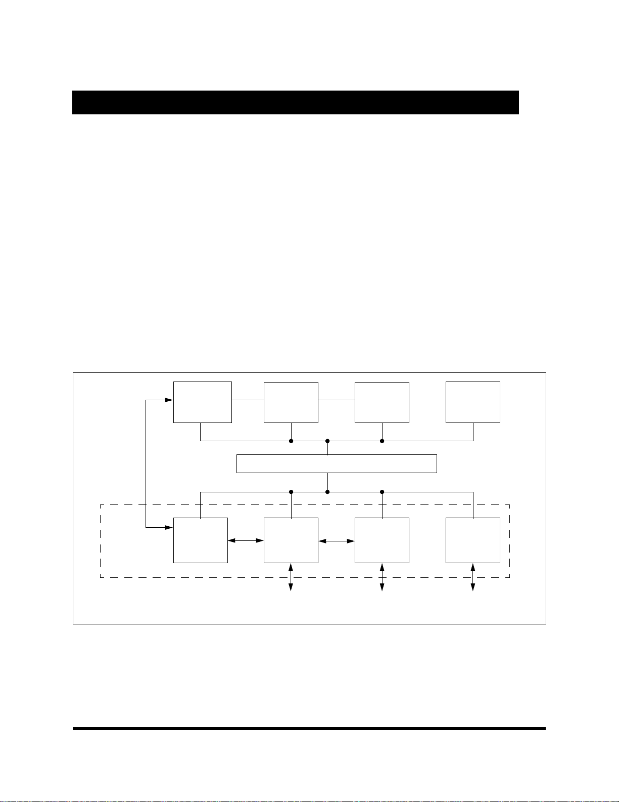
The MediaGX processor is divided into major functional blocks (as shown in Figure 1-1):
• Integer Unit
• Floating Point Unit (FPU)
• Write-Back Cache Unit
• Memory Management Unit (MMU)
• Internal Bus Interface Unit
• Integrated Functions
Instructions are executed in the integer unit and in
the floating point unit. The cache unit stores the
most recently used data and instructions and
provides fast access to this information for the
integer and floating point units.
Integer
Unit
FPU
Internal Bus Interface Unit
X-Bus
Integrated
Functions
GXm_db_v2.0 Cyrix Corporation Confidential Page 3
Graphics Memory Display PCI
Pipeline Controller Controller Controller
SDRAM Port Cx5520/Cx5530
(CRT/LCD TFT)
Figure 1-1 Internal Block Diagram
PCI Bus
Page 20

Architecture
1.1.1 Integer Unit
The integer unit consists of:
• Instruction Buffer
• Instruction Fetch
• Instruction Decoder and Execution
The superpipelined integer unit fetches, decodes,
and executes x86 instructions through the use of a
six-stage integer pipeline.
The instruction fetch pipeline stage generates,
from the on-chip cache, a continuous high-speed
instruction stream for use by the processor. Up to
128 bits of code are read during a single clock
cycle.
Branch prediction logic within the prefetch unit
generates a predicted target address for unconditional or conditional branch instructions. When a
branch instruction is detected, the instruction fetch
stage starts loading instructions at the predicted
address within a single clock cycle. Up to 48 bytes
of code are queued prior to the instruction decode
stage.
The instruction decode stage evaluates the code
stream provided by the instruction fetch stage and
determines the number of bytes in each instruction
and the instruction type. Instructions are processed
and decoded at a maximum rate of one instruction
per clock.
The address calculation function is super-pipelined
and contains two stages, AC1 and AC2. If the
instruction refers to a memory operand, AC1 calculates a linear memory address for the instruction.
The AC2 stage performs any required memory
management functions, cache accesses, and
register file accesses. If a floating point instruction
is detected by AC2, the instruction is sent to the
floating point unit for processing.
Write-back, the last stage of the integer unit,
updates the register file within the integer unit or
writes to the load/store unit within the memory
management unit.
1.1.2 Floating Point Unit
The FPU (Floating Point Unit) interfaces to the
integer unit and the cache unit through a 64-bit
bus. The FPU is x87-instruction-set compatible and
adheres to the IEEE-754 standard. Because
almost all applications that contain FPU instructions also contain integer instructions, the
MediaGX processor’s FPU achieves high performance by completing integer and FPU operations
in parallel.
FPU instructions are dispatched to the pipeline
within the integer unit. The address calculation
stage of the pipeline checks for memory management exceptions and accesses memory operands
for use by the FPU. Once the instructions and
operands have been provided to the FPU, the FPU
completes instruction execution independently of
the integer unit.
1.1.3 Write-Back Cache Unit
The 16KB write-back unified cache is a
data/instruction cache and is configured as fourway set associative. The cache stores up to 16KB
of code and data in 1024 cache lines.
The MediaGX processor provides the ability to allocate a portion of the L1 cache as a scratchpad,
which is used to accelerate the Virtual Systems
Architecture algorithms as well as for some
graphics operations.
The execution stage, under control of microcode,
executes instructions using the operands provided
by the address calculation stage.
Page 4 Cyrix Corporation Confidential GXm_db_v2.0
Page 21

Integrated Functions
1
1.1.4 Memory Management Unit
The memory management unit (MMU) translates
the linear address supplied by the integer unit into
a physical address to be used by the cache unit
and the internal bus interface unit. Memory
management procedures are x86-compatible,
adhering to standard paging mechanisms.
The MMU also contains a load/store unit that is
responsible for scheduling cache and external
memory accesses. The load/store unit incorporates two performance-enhancing features:
•
Load-store reordering
memory reads required by the integer unit over
writes to external memory.
•
Memory-read bypassing
unnecessary memory reads by using valid data
from the execution unit.
that gives priority to
that eliminates
1.1.5 Internal Bus Interface Unit
The internal bus interface unit provides a bridge
from the MediaGX processor to the integrated
system functions (i.e., memory subsystem, display
controller, graphics pipeline) and the PCI bus interface.
When external memory access is required, the
physical address is calculated by the memory
management unit and then passed to the internal
bus interface unit, which translates the cycle to an
X-Bus cycle (the X-Bus is a Cyrix proprietary
internal bus which provides a common interface for
all of the system modules). The X-Bus memory
cycle now is arbitrated between other pending XBus memory requests to the SDRAM controller
before completing.
In addition, the internal bus interface unit provides
configuration control for up to 20 different regions
within system memory with separate controls for
read access, write access, cacheability, and PCI
access.
1.2 Integrated Functions
The MediaGX processor integrate s the foll owi ng
functions traditionally implemented using external
devices:
• High-performance 2D graphics accelerator
• Separate CRT and TFT data paths from the
display controller
• SDRAM memory controller
• PCI bridge
The processor has also been enhanced to support
Cyrix’s proprietary Virtual System Architecture
(VSA) implementation.
The MediaGX processor implements a Unified
Memory Architecture (UMA). By using Cyrix’s
Display Compression Technology™ (DCT), the
performance degradation inh erent in tra di tio nal
UMA systems is elimi nated.
1.2.1 Graphics Accelerator
The graphics accelerator is a full-featured GUI
(Graphical User Interface) accelerator. The
graphics pipeline implements a bitBLT engine for
frame buffer bitBLTs and rectangular fills. Additional instructions in the integer unit may be
processed, as the bitBLT engine assists the CPU in
the bitBLT operations that take place between
system memory and the frame buffer. This combination of hardware and software is used by the
display driver to provide very fast transfers in both
directions between system memory and the frame
buffer. The bitBLT engine also draws randomlyoriented vectors, and scanlines for polygon fill. All
of the pipeline operations described in the following
list can be applied to any bitBLT operation.
GXm_db_v2.0 Cyrix Corporation Confidential Page 5
Page 22

Integrated Functions
•
Pattern Memory.
monochrome, or 8x1 color pattern.
•
Color Expansion.
bitmaps to full-depth 8- or 16-bit colors.
•
Transparency.
ground pixels for transparent text.
•
Raster Operations.
combines source, destination, and pattern
bitmaps.
Render with 8x8 dither, 8x8
Expand monochrome
Suppresses drawing of back-
Boolean operation
1.2.2 Display Controller
The display port is a direct interface to the
Cx5520/Cx5530 which drives a TFT flat panel
display, LCD panel, or a CRT display.
The display controller (video generator) retrieves
image data from the frame buffer region of
memory, performs a color-look-up if required,
inserts the cursor overlay into the pixel stream,
generates display timing, and formats the pixel
data for output to a variety of display devices. The
display controller contains Display Compression
Technology (DCT) that allows the MediaGX
processor to refresh the display from a
compressed copy of the frame buffer. DCT typically
decreases the screen-refresh bandwidth requirement by a factor of 15 to 20, further minimizing
bandwidth contention.
1.2.3 XpressRAM™ Memory
Subsystem
The memory controller drives a 64-bit SDRAM port
directly. The SDRAM memory array contains both
the main system memory and the graphics frame
buffer. Up to four module banks of SDRAM are
supported. Each module bank will have two or four
component banks depending on the memory size
and organization. The maximum configuration is
four module banks with four component banks
providing a total of 16 open banks. The maximum
memory size is 1GB.
The memory controller handles multiple requests
for memory data from the MediaGX processor, the
graphics accelerator and the display controller. The
memory controller contains extensive buffering
logic that helps minimize contention for memory
bandwidth between graphics and CPU re que sts.
The memory controller cooperates with the internal
bus controller to determine the cacheability of all
memory references.
1.2.4 PCI Controller
The MediaGX processor incorporates a full-function PCI interface module that includes the PCI
arbiter. All accesses to external I/O devices are
sent over the PCI bus, although most memory
accesses are serviced by the SDRAM controller.
The Internal Bus Interface Unit contains address
mapping logic that determines if memory accesses
are targeted for the SDRAM or for the PCI bus.
Page 6 Cyrix Corporation Confidential GXm_db_v2.0
Page 23
System Designs
1
1.3 System Designs
The Cyrix MediaGX™ Integrated Subsystem with
MMX™ support consists of two chips, the
MediaGX MMX-Enhanced Processor and the
Cx5520™ or Cx5530™ I/O Companion. The
subsystem provides high performance using 64-bit
x86 processing. The two chips integrate video,
audio and memory interface functions normally
performed by external hardware.
As described in separate manuals, the Cx5520 and
Cx5530 enable the full features of the MediaGX
processor with MMX support. These features
MD[63:0]
SDRAM
Clocks
USB
(2 Ports)
Speakers
CD
ROM
Audio
AC97
CODEC
System
Clocks
Cx55x0™
I/O Companion
include full VGA and VESA video, 16-bit stereo
sound, IDE interface, ISA interface, SMM power
management, and AT compatibility logic. In addition, the newer Cx5530 provides an Ultra DMA/33
interface, MPEG2 assist, and AC97 Version 2.0
compliant audio.
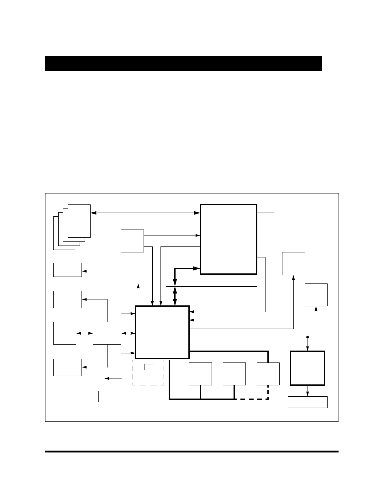
Figure 1-2 shows a basic block system diagram
(refer to Figure 2-4 on page 34 for detailed
subsystem interconnection signals). It includes the
Cyrix Cx9210™ Dual-Scan Flat Panel Display
Controller for designs that need to interface to a
DSTN panel (instead of TFT panel).
SDRAM
Port
MediaGX™
MMX™-Enhanced
Processor
Serial
Packet
PCI Interface
Graphics Data
Video Data
Analog RGB
Digital RGB
IDE Control
YUV Port
(Video)
RGB Port
(Graphics)
PCI Bus
(to TFT or DSTN Panel)
CRT
TF T
Panel
Microphone
GPIO
DC-DC & Battery
Dashed lines denote Cx5520 application.
Note:
14.31818
MHz Crystal
ISA Bus
Super
I/O
BIOS
IDE
Devices
Cx9210™
DSTN
Controller
DSTN Panel
Figure 1-2 System Block Diagram
GXm_db_v2.0 Cyrix Corporation Confidential Page 7
Page 24
System Designs
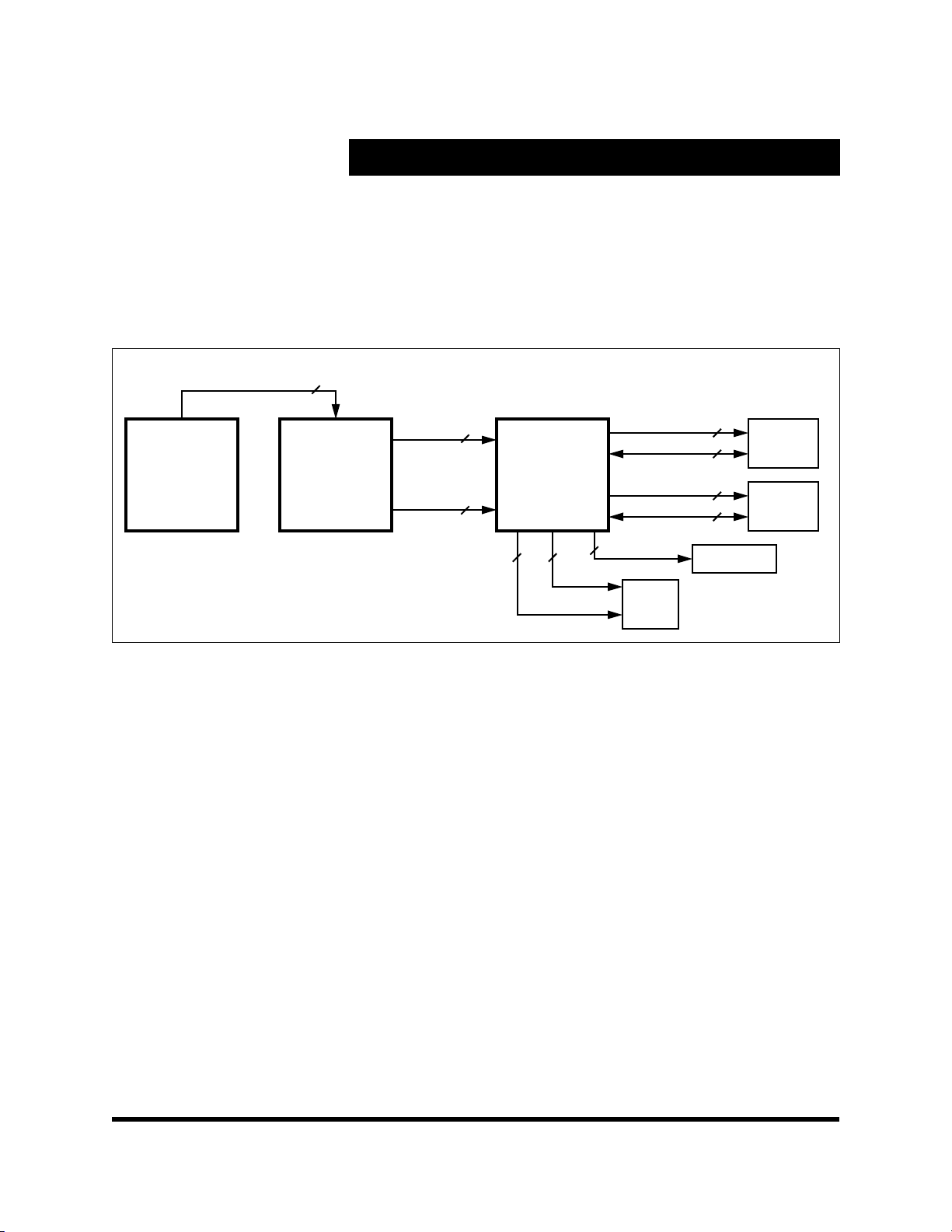
The Cx9210 converts the digital RGB output of a
Cx5520 or Cx5530 I/O Companion chip to the
digital output suitable for driving a dual-scan color
STN (DSTN) flat panel LCD. It connects to the
digital RGB output of a MediaGX™ processor or
Cx55
x
0 and drives the graphics data onto a dual-
Pixel Data
MediaGX™
Processor
18
x
Cx55
0™
I/O
Companion
Pixel Port
Control
Figure 1-3 Cx9210 Interface System Diagram
scan flat panel LCD. It can drive all standard dualscan color STN flat panels up to 1024x768 resolution. Figure 1-3 shows an example of a Cx9210
interface in a typical MediaGX Integrated
Subsystem.
23
4
Cx9210™
DSTN
Controller
316
Clocks
Panel Data
3
Control
Addr Control
DRAM Data
Addr Control
DRAM Data
DSTN
LCD
13
16
13
16
LCD Power
DRAM A
256K x 16
DRAM B
256K x 16
Page 8 Cyrix Corporation Confidential GXm_db_v2.0
Page 25
2 Signal Definitions
MediaGX™ MMX™-Enhanced Processor
Integrated x86 Solution with MMX™ Support
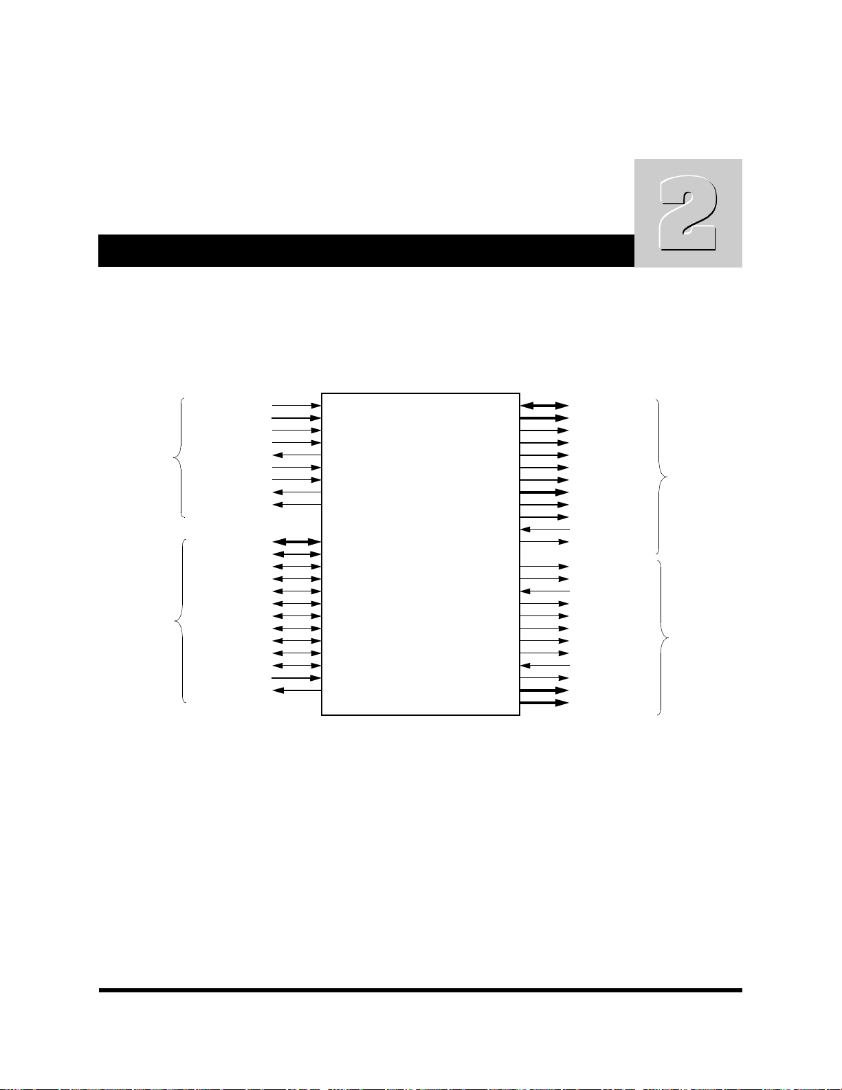
This section describes the external interface of the
MediaGX processor. Figure 2-1 shows the signals
SYSCLK
CLKMODE[2:0]
RESET
System
Interface
Signals
PCI
Interface
Signals
INTR
IRQ13
SMI#
SUSP#
SUSPA#
SERIALP
AD[31:0]
C/BE[3:0]#
PAR
FRAME#
IRDY#
TRDY#
STOP#
LOCK#
DEVSEL#
PERR#
SERR#
REQ[2:0]#
GNT[2:0]#
MediaGX™
MMX™-Enhanced
Processor
organized by their functional interface groups
(internal test and electrical pins are not shown).
MD[63:0]
MA[12:0]
BA[1:0]
RASA#, RASB#
CASA#, CASB#
CS[3:0]#
WEA#, WEB#
DQM[7:0]
CKEA, CKEB
SDCLK[3:0]
SDCLK_IN
SDCLK_OUT
PCLK
VID_CLK
DCLK
CRT_HSYNC
CRT_VSYNC
FP_HSYNC
FP_VSYNC
ENA_DISP
VID_RDY
VID_VAL
VID_DATA[7:0]
PIXEL[17:0]
Memory
Controller
Interface
Signals
Video
Interface
Signals
Figure 2-1 Functional Block Diagram
GXm_db_v2.0 Cyrix Corporation Confidential Page 9
Page 26
Pin Assignments
2.1 Pin Assignments
The MediaGX MMX-Enhanced processor is available in two packages, a 352 BGA package and a
320 SPGA package.
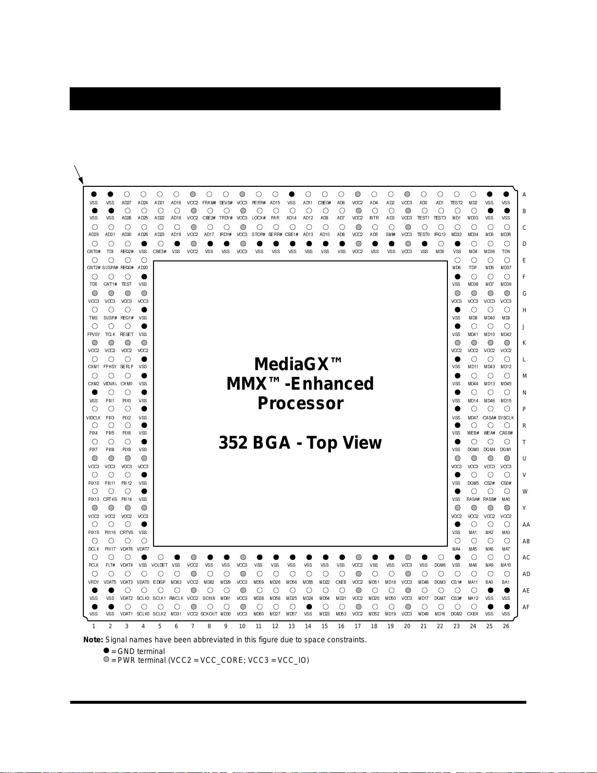
The pin assignment for the 352 BGA is shown in
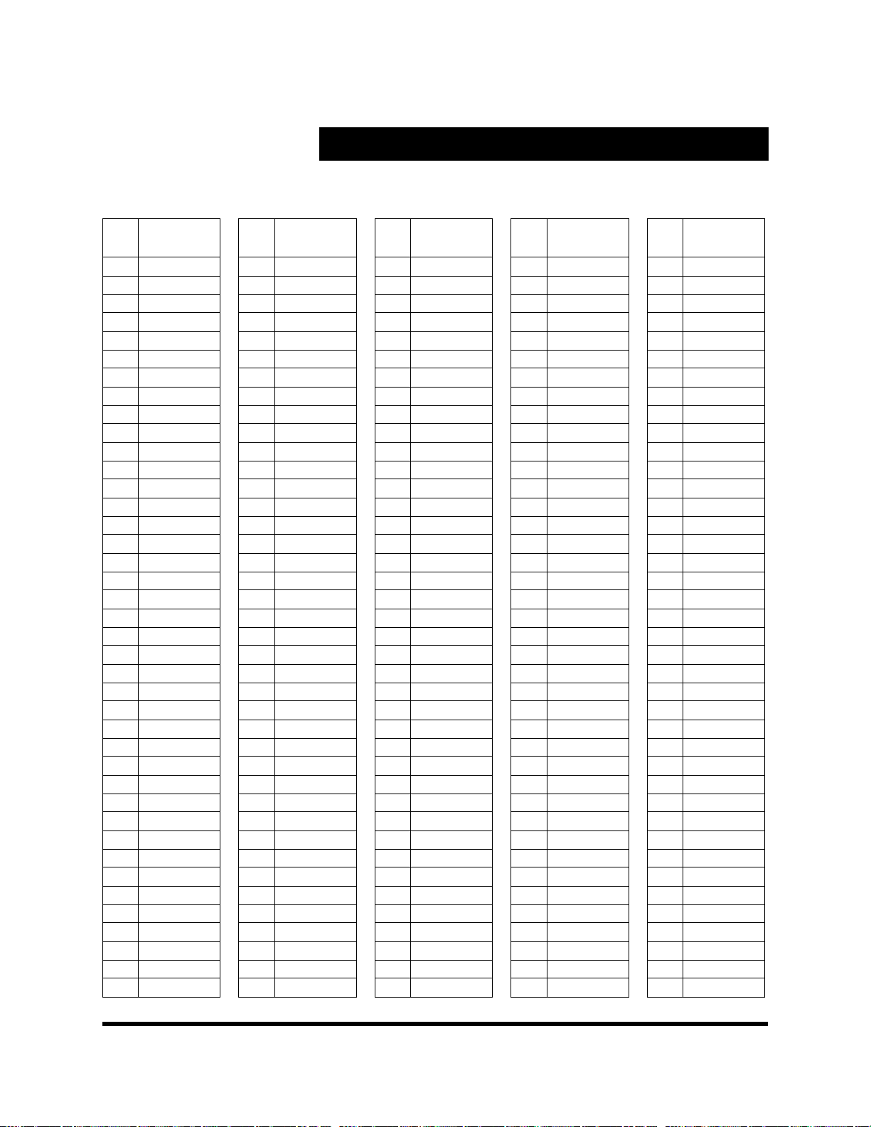
Figure 2-2. Tables 2-2 and 2-3 are pin assignment
lists for the 352 BGA sorted by pin number and
alphabetically by signal name, respectively.
The 320 SPGA pin assignment is shown in Figure
2-3. Tables 2-4 and 2-5 are pin assignment lists for
the 320 SPGA sorted by pin number and alphabetically by signal name, respectively.
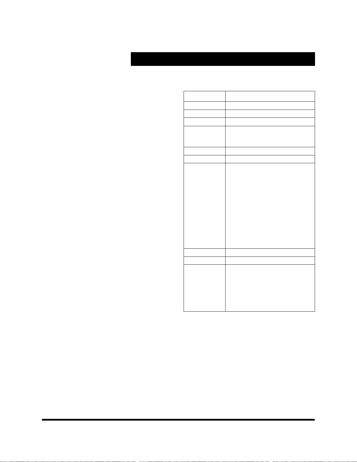
Abbreviations used in Tables 2-4 through 2-5 are
shown in Ta ble 2-1.
Section 2.2 on page 21 describes the signals which
are grouped according their functional group.
Table 2-1 Pin Type Definitions
Mnemonic Definition
I Standard input pin.
I/O Bidirectional pin.
O Totem-pole output.
OD Open-drain output structure that
allows multiple devices to share the
pin in a wired-OR configuration
PU Pull-up resistor
PD Pull-down resistor
s/t/s Sustained tristate, an active-low
tristate signal owned and driven by
one and only one agent at a time.
The agent that drives an s/ t/s pin low
must drive it high for at least one
clock before letting it float. A new
agent cannot start driving an s/t/s
signal any s ooner than one clock
after the previous owner lets it float.
A pull-up resistor is required to sus-
tain the inactive state until another
agent drives it, and must be pro-
vided by the central resource.
VCC (PWR) Power pin.
VSS (GND) Ground pin
# The "#" symbol at th e end of a signa l
name indicates that the active, or
asserted state occurs when the sig-
nal is at a low voltage level. When
"#" is not present after the signal
name, the signal is asse rted when at
a high voltage level.
Page 10 Cyrix Corporation Confidential GXm_db_v2.0
Page 27
Index Corner
g
Pin Assignments
2
1234567891011121314151617181920
A
966 966 $' $' $' $' 9&& )5$0 '(96 9&& 3(55 $' 966 $' &%( $' 9&& $' $' 9&& $' $' 7(67 0' 966 966
B
966 966 $' $' $' $' 9&& &%( 75'< 9&& /2&. 3$5 $' $' $' $' 9&& ,175 $' 9&& 7(67 7(67 0' 0' 966 966
C
$' $' $' $' $' $' 9&& $' ,5'< 9&& 6723 6(55 &%( $' $' $' 9&& $' 60, 9&& 7(67 ,54 0' 0' 0' 0'
D
*17 7', 5(4 966 &%( 966 9&& 966 966 9&& 966 966 966 966 966 966 9&& 966 966 9&& 966 0' 966 0' 0' 7'1
E
*17 6863$ 5(4 $' 0' 7'3 0' 0'
F
7' *17 7(67 966 966 0' 0' 0'
G
9&& 9&& 9&& 9&& 9&& 9&& 9&& 9&&
H
706 6863 5(4 966 966 0' 0' 0'
J
)396< 7&/. 5(6(7 966 966 0' 0' 0'
K
9&& 9&& 9&& 9&& 9&& 9&& 9&& 9&&
L
&.0 )3+6< 6(5/3 966 966 0' 0' 0'
M
&.0 9,'9$/ &.0 966 966 0' 0' 0'
N
966 3,; 3,; 966 966 0' 0' 0'
P
9,'&/. 3,; 3,; 966 966 0' &$6$ 6<6&/.
R
3,; 3,; 3,; 966 966 :(% :($ &$6%
T
3,; 3,; 3,; 966 966 '40 '40 '40
U
9&& 9&& 9&& 9&& 9&& 9&& 9&& 9&&
V
3,; 3,; 3,; 966 966 '40 &6 &6
W
3,; &57+6 3,; 966 966 5$6$ 5$6% 0$
Y
9&& 9&& 9&& 9&& 9&& 9&& 9&& 9&&
AA
3,; 3,; &5796 966 966 0$ 0$ 0$
AB
'&/. 3,; 9'$7 9'$7 0$ 0$ 0$ 0$
AC
3&/. )/7 9'$7 966 92/'(7 966 9&& 966 966 9&& 966 966 966 966 966 966 9&& 966 966 9&& 966 '40 966 0$ 0$ 0$
AD
95'< 9'$7 9'$7 9'$7 (',63 0' 9&& 0' 0' 9&& 0' 0' 0' 0' 0' &.(% 9&& 0' 0' 9&& 0' '40 &6 0$ %$ %$
AE
966 966 9'$7 6&/. 6&/. 5:&/. 9&& 6&.,1 0' 9&& 0' 0' 0' 0' 0' 0' 9&& 0' 0' 9&& 0' '40 &6 0$ 966 966
AF
966 966 9'$7 6&/. 6&/. 0' 9&& 6&.287 0' 9&& 0' 0' 0' 966 0' 0' 9&& 0' 0' 9&& 0' 0' '40 &.($ 966 966
1234567891011121314151617181920
Note:
nal names have been abbreviated in this figure due to space constraints.
Si
352 BGA - Top View
MediaGX™
MMX™-Enhanced
Processor
21 22 23 24 25 26
21 22 23 24 25 26
= GND terminal
= PWR terminal (VCC2 = VCC_CORE; VCC3 = VCC_IO)
Figure 2-2 352 BGA Pin Assignment Diagram
A
B
C
D
E
F
G
H
J
K
L
M
N
P
R
T
U
V
W
Y
AA
AB
AC
AD
AE
AF
GXm_db_v2.0 Cyrix Corporation Confidential Page 11
Page 28
Pin Assignments
Table 2-2 352 BGA Pin Assignments - Sorted by Pin Number
Pin
No. Signal Name
A1 VSS
A2 VSS
A3 AD27
A4 AD24
A5 AD21
A6 AD16
A7 VCC2
A8 FRAME#
A9 DEVSEL#
A10 VCC3
A11 PERR#
A12 AD15
A13 VSS
A14 AD11
A15 C/BE0#
A16 AD6
A17 VCC2
A18 AD4
A19 AD2
A20 VCC3
A21 AD0
A22 AD1
A23 TEST2
A24 MD2
A25 VSS
A26 VSS
B1 VSS
B2 VSS
B3 AD28
B4 AD25
B5 AD22
B6 AD18
B7 VCC2
B8 C/BE2#
B9 TRDY#
B10 VCC3
B11 LOCK#
B12 PAR
B13 AD14
B14 AD12
Pin
No. Signal Name
B15 AD9
B16 AD7
B17 VCC2
B18 INTR
B19 AD3
B20 VCC3
B21 TEST1
B22 TEST3
B23 MD1
B24 MD33
B25 VSS
B26 VSS
C1 AD29
C2 AD31
C3 AD30
C4 AD26
C5 AD23
C6 AD19
C7 VCC2
C8 AD17
C9 IRDY#
C10 VCC3
C11 STOP#
C12 SERR#
C13 C/BE1#
C14 AD13
C15 AD10
C16 AD8
C17 VCC2
C18 AD5
C19 SMI#
C20 VCC3
C21 TEST0
C22 IRQ13
C23 MD32
C24 MD34
C25 MD3
C26 MD35
D1 GNT0#
D2 TDI
Pin
No. Signal Name
D3 REQ2#
D4 VSS
D5 C/BE3#
D6 VSS
D7 VCC2
D8 VSS
D9 VSS
D10 VCC3
D11 VSS
D12 VSS
D13 VSS
D14 VSS
D15 VSS
D16 VSS
D17 VCC2
D18 VSS
D19 VSS
D20 VCC3
D21 VSS
D22 MD0
D23 VSS
D24 MD4
D25 MD36
D26 TDN
E1 GNT2#
E2 SUSPA#
E3 REQ0#
E4 AD20
E23 MD6
E24 TDP
E25 MD5
E26 MD37
F1 TDO
F2 GNT1#
F3 TEST
F4 VSS
F23 VSS
F24 MD38
F25 MD7
F26 MD39
Pin
No. Signal Name
G1 VCC3
G2 VCC3
G3 VCC3
G4 VCC3
G23 VCC3
G24 VCC3
G25 VCC3
G26 VCC3
H1 TMS
H2 SUSP#
H3 REQ1#
H4 VSS
H23 VSS
H24 MD8
H25 MD40
H26 MD9
J1 FP_VSYNC
J2 TCLK
J3 RESET
J4 VSS
J23 VSS
J24 MD41
J25 MD10
J26 MD42
K1 VCC2
K2 VCC2
K3 VCC2
K4 VCC2
K23 VCC2
K24 VCC2
K25 VCC2
K26 VCC2
L1 CLKMODE1
L2 FP_HSYNC
L3 SERIALP
L4 VSS
L23 VSS
L24 MD11
L25 MD43
L26 MD12
Pin
No. Signal Name
M1 CLKMODE2
M2 VID_VAL
M3 CLKMODE0
M4 VSS
M23 VSS
M24 MD44
M25 MD13
M26 MD45
N1 VSS
N2 PIXEL1
N3 PIXEL0
N4 VSS
N23 VSS
N24 MD14
N25 MD46
N26 MD15
P1 VID_CLK
P2 PIXEL3
P3 PIXEL2
P4 VSS
P23 VSS
P24 MD47
P25 CASA#
P26 SYSCLK
R1 PIXEL4
R2 PIXEL5
R3 PIXEL6
R4 VSS
R23 VSS
R24 WEB#
R25 WEA#
R26 CASB#
T1 PIXEL7
T2 PIXEL8
T3 PIXEL9
T4 VSS
T23 VSS
T24 DQM0
T25 DQM4
T26 DQM1
Page 12 Cyrix Corporation Confidential GXm_db_v2.0
Page 29
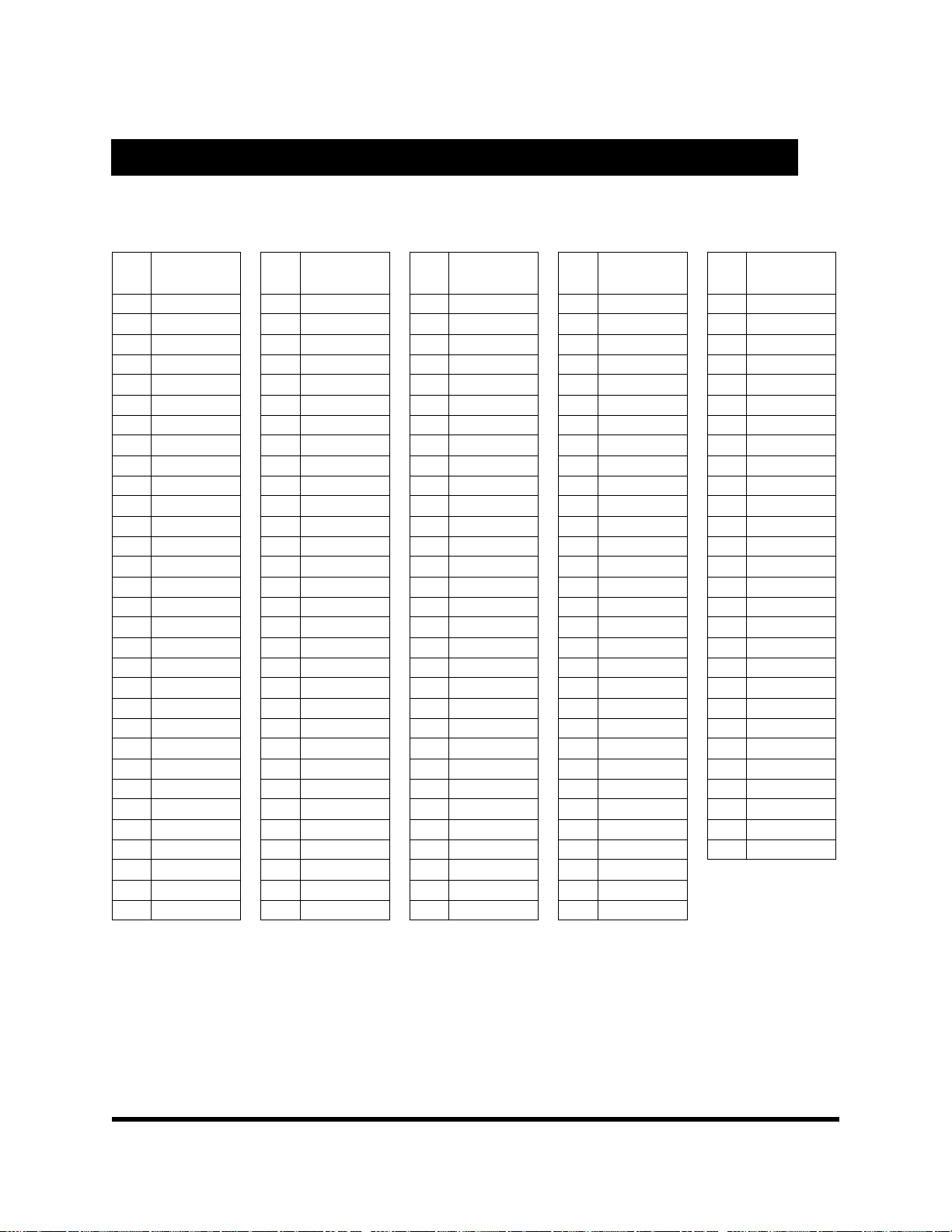
Table 2-2 352 BGA Pin Assignments - Sorted by Pin Number (cont.)
Pin Assignments
2
Pin
No. Signal Name
U1 VCC3
U2 VCC3
U3 VCC3
U4 VCC3
U23 VCC3
U24 VCC3
U25 VCC3
U26 VCC3
V1 PIXEL10
V2 PIXEL11
V3 PIXEL12
V4 VSS
V23 VSS
V24 DQM5
V25 CS2#
V26 CS0#
W1 PIXEL13
W2 CRT_HSYNC
W3 PIXEL14
W4 VSS
W23 VSS
W24 RASA#
W25 RASB#
W26 MA0
Y1 VCC2
Y2 VCC2
Y3 VCC2
Y4 VCC2
Y23 VCC2
Y24 VCC2
Y25 VCC2
Pin
No. Signal Name
Y26 VCC2
AA1 PIXEL15
AA2 PIXEL16
AA3 CRT_VSYNC
AA4 VSS
AA23 VSS
AA24 MA1
AA25 MA2
AA26 MA3
AB1 DCLK
AB2 PIXEL17
AB3 VID_DATA6
AB4 VID_DATA7
AB23 MA4
AB24 MA5
AB25 MA6
AB26 MA7
AC1 PCLK
AC2 FLT#
AC3 VID_DATA4
AC4 VSS
AC5 VOLDET
AC6 VSS
AC7 VCC2
AC8 VSS
AC9 VSS
AC10 VCC3
AC11 VSS
AC12 VSS
AC13 VSS
AC14 VSS
Pin
No. Signal Name
AC15 VSS
AC16 VSS
AC17 VCC2
AC18 VSS
AC19 VSS
AC20 VCC3
AC21 VSS
AC22 DQM6
AC23 VSS
AC24 MA8
AC25 MA9
AC26 MA10
AD1 VID_RDY
AD2 VID_DATA5
AD3 VID_DATA3
AD4 VID_DATA0
AD5 ENA_DISP
AD6 MD63
AD7 VCC2
AD8 MD62
AD9 MD29
AD10 VCC3
AD11 MD59
AD12 MD26
AD13 MD56
AD14 MD55
AD15 MD22
AD16 CKEB
AD17 VCC2
AD18 MD51
AD19 MD18
Pin
No. Signal Name
AD20 VCC3
AD21 MD48
AD22 DQM3
AD23 CS1#
AD24 MA11
AD25 BA0
AD26 BA1
AE1 VSS
AE2 VSS
AE3 VID_DATA2
AE4 SDCLK3
AE5 SDCLK1
AE6 RW_CLK
AE7 VCC2
AE8 SDCLK_IN
AE9 MD61
AE10 VCC3
AE11 MD28
AE12 MD58
AE13 MD25
AE14 MD24
AE15 MD54
AE16 MD21
AE17 VCC2
AE18 MD20
AE19 MD50
AE20 VCC3
AE21 MD17
AE22 DQM7
AE23 CS3#
AE24 MA12
Pin
No. Signal Name
AE25 VSS
AE26 VSS
AF1 VSS
AF2 VSS
AF3 VID_DATA1
AF4 SDCLK0
AF5 SDCLK2
AF6 MD31
AF7 VCC2
AF8 SDCLK_OUT
AF9 MD30
AF10 VCC3
AF11 MD60
AF12 MD27
AF13 MD57
AF14 VSS
AF15 MD23
AF16 MD53
AF17 VCC2
AF18 MD52
AF19 MD19
AF20 VCC3
AF21 MD49
AF22 MD16
AF23 DQM2
AF24 CKEA
AF25 VSS
AF26 VSS
GXm_db_v2.0 Cyrix Corporation Confidential Page 13
Page 30
Pin Assignments
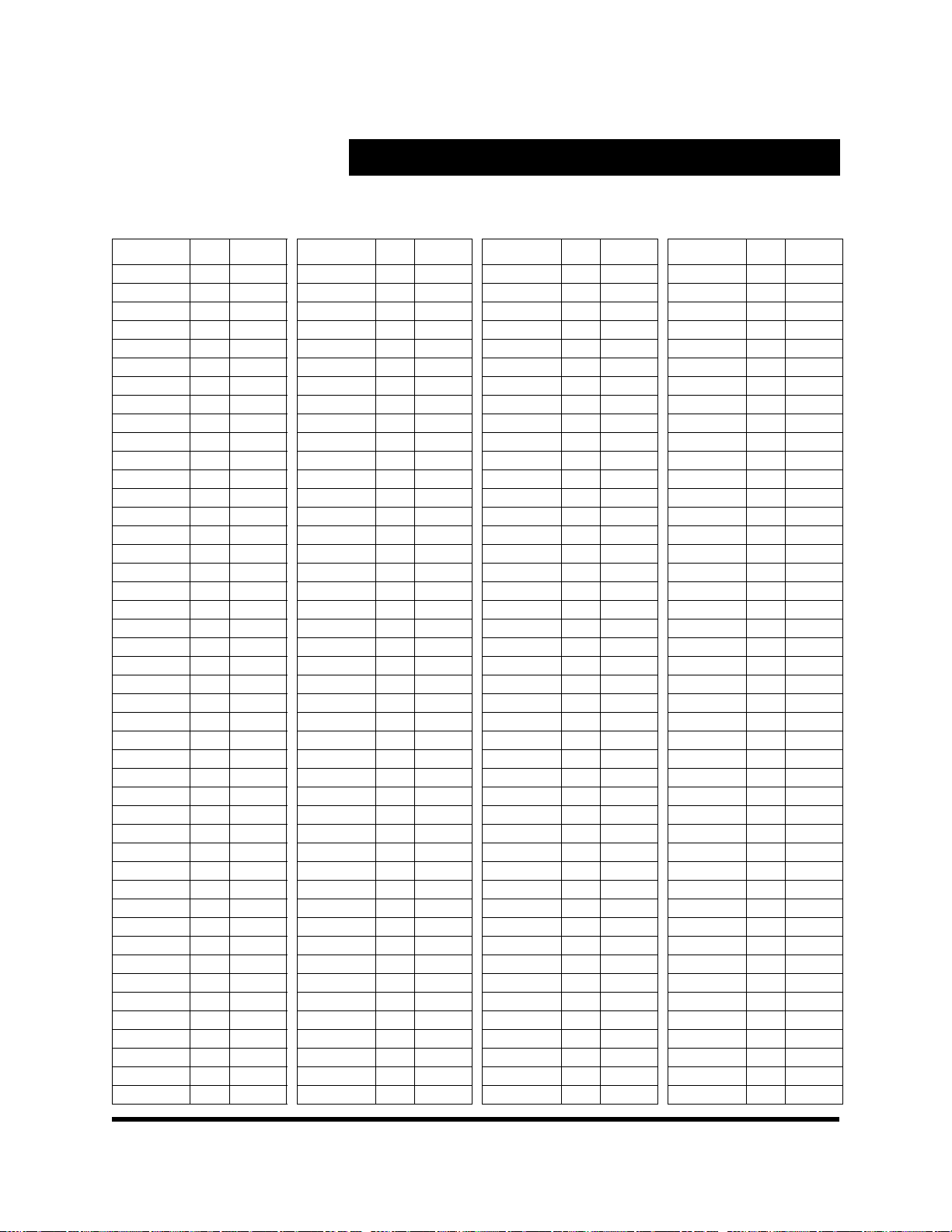
Table 2-3 352 BGA Pin Assignments - Sorted Alphabetically by Signal Name
Signal Name Type Pin No.
AD0 I/O A21
AD1 I/O A22
AD2 I/O A19
AD3 I/O B19
AD4 I/O A18
AD5 I/O C18
AD6 I/O A16
AD7 I/O B16
AD8 I/O C16
AD9 I/O B15
AD10 I/O C15
AD11 I/O A14
AD12 I/O B14
AD13 I/O C14
AD14 I/O B13
AD15 I/O A12
AD16 I/O A6
AD17 I/O C8
AD18 I/O B6
AD19 I/O C6
AD20 I/O E4
AD21 I/O A5
AD22 I/O B5
AD23 I/O C5
AD24 I/O A4
AD25 I/O B4
AD26 I/O C4
AD27 I/O A3
AD28 I/O B3
AD29 I/O C1
AD30 I/O C3
AD31 I/O C2
BA0 O AD25
BA1 O AD26
CASA# O P25
CASB# O R26
C/BE0# I/O A15
C/BE1# I/O C13
C/BE2# I/O B8
C/BE3# I/O D5
CKEA O AF24
CKEB O AD16
CLKMODE0 I M3
CLKMODE1 I L1
CLKMODE2 I M1
Signal Name Type Pin No.
CRT_HSYNC O W2
CRT_VSYNC O AA3
CS0# O V26
CS1# O AD23
CS2# O V25
CS3# O AE23
DCLK I AB1
DEVSEL# s/t/s A9 (PU)
DQM0 O T24
DQM1 O T26
DQM2 O AF23
DQM3 O AD22
DQM4 O T25
DQM5 O V24
DQM6 O AC22
DQM7 O AE22
ENA_DISP O AD5
FLT# I AC2
FP_HSYNC O L2
FP_VSYNC O J1
FRAME# s/t/s A8 (PU)
GNT0# O D1
GNT1# O F2
GNT2# O E1
INTR I B18
IRDY# s/t/s C9 (PU)
IRQ13 O C22
LOCK# s/t/s B11 (PU)
MA0 O W26
MA1 O AA24
MA2 O AA25
MA3 O AA26
MA4 O AB23
MA5 O AB24
MA6 O AB25
MA7 O AB26
MA8 O AC24
MA9 O AC25
MA10 O AC26
MA11 O AD24
MA12 O AE24
MD0 I/O D22
MD1 I/O B23
MD2 I/O A24
MD3 I/O C25
Signal Name Type Pin No.
MD4 I/O D24
MD5 I/O E25
MD6 I/O E23
MD7 I/O F25
MD8 I/O H24
MD9 I/O H26
MD10 I/O J25
MD11 I/O L24
MD12 I/O L26
MD13 I/O M25
MD14 I/O N24
MD15 I/O N26
MD16 I/O AF22
MD17 I/O AE21
MD18 I/O AD19
MD19 I/O AF19
MD20 I/O AE18
MD21 I/O AE16
MD22 I/O AD15
MD23 I/O AF15
MD24 I/O AE14
MD25 I/O AE13
MD26 I/O AD12
MD27 I/O AF12
MD28 I/O AE11
MD29 I/O AD9
MD30 I/O AF9
MD31 I/O AF6
MD32 I/O C23
MD33 I/O B24
MD34 I/O C24
MD35 I/O C26
MD36 I/O D25
MD37 I/O E26
MD38 I/O F24
MD39 I/O F26
MD40 I/O H25
MD41 I/O J24
MD42 I/O J26
MD43 I/O L25
MD44 I/O M24
MD45 I/O M26
MD46 I/O N25
MD47 I/O P24
MD48 I/O AD21
Signal Name Type Pin No.
MD49 I/O AF21
MD50 I/O AE19
MD51 I/O AD18
MD52 I/O AF18
MD53 I/O AF16
MD54 I/O AE15
MD55 I/O AD14
MD56 I/O AD13
MD57 I/O AF13
MD58 I/O AE12
MD59 I/O AD11
MD60 I/O AF11
MD61 I/O AE9
MD62 I/O AD8
MD63 I/O AD6
PAR I/O B12
PCLK O AC1
PERR# s/t/s A11 (PU)
PIXEL0 O N3
PIXEL1 O N2
PIXEL2 O P3
PIXEL3 O P2
PIXEL4 O R1
PIXEL5 O R2
PIXEL6 O R3
PIXEL7 O T1
PIXEL8 O T2
PIXEL9 O T3
PIXEL10 O V1
PIXEL11 O V2
PIXEL12 O V3
PIXEL13 O W1
PIXEL14 O W3
PIXEL15 O AA1
PIXEL16 O AA2
PIXEL17 O AB2
RASA# O W24
RASB# O W25
REQ0# I E3 (PU)
REQ1# I H3 (PU)
REQ2# I D3 (PU)
RESET I J3
RW_CLK O AE6
SDCLK_IN I AE8
SDCLK_OUT O AF8
Page 14 Cyrix Corporation Confidential GXm_db_v2.0
Page 31
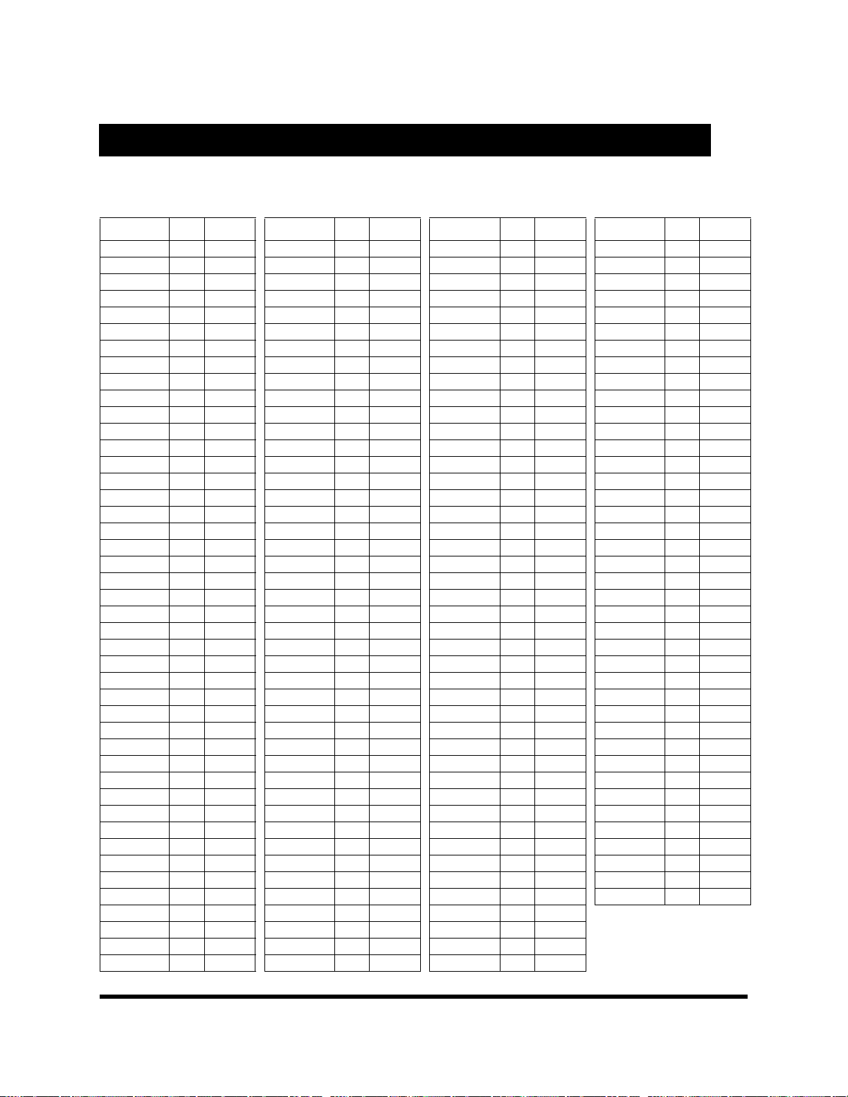
Pin Assignments
Table 2-3 352 BGA Pin Assignments - Sorted Alphabetically by Signal Name (cont.)
2
Signal Name Type Pin No.
SDCLK0 O AF4
SDCLK1 O AE5
SDCLK2 O AF5
SDCLK3 O AE4
SERIALP O L3
SERR# OD C12 (PU)
SMI# I C19
STOP# s/t/s C11 (PU)
SUSP# I H2 (PU)
SUSPA# O E2
SYSCLK I P26
TCLK I J2 (PU)
TDI I D2 (PU)
TDN O D26
TDO O F1
TDP O E24
TEST I F3 (PD)
TEST0 O C21
TEST1 O B21
TEST2 O A23
TEST3 O B22
TMS I H1 (PU)
TRDY# s/t/s B9 (PU)
VCC2 PWR A7
VCC2 PWR A17
VCC2 PWR B7
VCC2 PWR B17
VCC2 PWR C7
VCC2 PWR C17
VCC2 PWR D7
VCC2 PWR D17
VCC2 PWR K1
VCC2 PWR K2
VCC2 PWR K3
VCC2 PWR K4
VCC2 PWR K23
VCC2 PWR K24
VCC2 PWR K25
VCC2 PWR K26
VCC2 PWR Y1
VCC2 PWR Y2
VCC2 PWR Y3
VCC2 PWR Y4
VCC2 PWR Y23
Signal Name Type Pin No.
VCC2 PWR Y24
VCC2 PWR Y25
VCC2 PWR Y26
VCC2 PWR AC7
VCC2 PWR AC17
VCC2 PWR AD7
VCC2 PWR AD17
VCC2 PWR AE7
VCC2 PWR AE17
VCC2 PWR AF7
VCC2 PWR AF17
VCC3 PWR A10
VCC3 PWR A20
VCC3 PWR B10
VCC3 PWR B20
VCC3 PWR C10
VCC3 PWR C20
VCC3 PWR D10
VCC3 PWR D20
VCC3 PWR G1
VCC3 PWR G2
VCC3 PWR G3
VCC3 PWR G4
VCC3 PWR G23
VCC3 PWR G24
VCC3 PWR G25
VCC3 PWR G26
VCC3 PWR U1
VCC3 PWR U2
VCC3 PWR U3
VCC3 PWR U4
VCC3 PWR U23
VCC3 PWR U24
VCC3 PWR U25
VCC3 PWR U26
VCC3 PWR AC10
VCC3 PWR AC20
VCC3 PWR AD10
VCC3 PWR AD20
VCC3 PWR AE10
VCC3 PWR AE20
VCC3 PWR AF10
VCC3 PWR AF20
VID_CLK O P1
Signal Name Type Pin No.
VID_DATA0 O AD4
VID_DATA1 O AF3
VID_DATA2 O AE3
VID_DATA3 O AD3
VID_DATA4 O AC3
VID_DATA5 O AD2
VID_DATA6 O AB3
VID_DATA7 O AB4
VID_RDY I AD1
VID_VAL O M2
VOLDET O AC5
VSS GND A1
VSS GND A2
VSS GND A13
VSS GND A25
VSS GND A26
VSS GND B1
VSS GND B2
VSS GND B25
VSS GND B26
VSS GND D4
VSS GND D6
VSS GND D8
VSS GND D9
VSS GND D11
VSS GND D12
VSS GND D13
VSS GND D14
VSS GND D15
VSS GND D16
VSS GND D18
VSS GND D19
VSS GND D21
VSS GND D23
VSS GND F4
VSS GND F23
VSS GND H4
VSS GND H23
VSS GND J4
VSS GND J23
VSS GND L4
VSS GND L23
VSS GND M4
VSS GND M23
Signal Name Type Pin No.
VSS GND N1
VSS GND N4
VSS GND N23
VSS GND P4
VSS GND P23
VSS GND R4
VSS GND R23
VSS GND T4
VSS GND T23
VSS GND V4
VSS GND V23
VSS GND W4
VSS GND W23
VSS GND AA4
VSS GND AA23
VSS GND AC4
VSS GND AC6
VSS GND AC8
VSS GND AC9
VSS GND AC11
VSS GND AC12
VSS GND AC13
VSS GND AC14
VSS GND AC15
VSS GND AC16
VSS GND AC18
VSS GND AC19
VSS GND AC21
VSS GND AC23
VSS GND AE1
VSS GND AE2
VSS GND AE25
VSS GND AE26
VSS GND AF1
VSS GND AF2
VSS GND AF14
VSS GND AF25
VSS GND AF26
WEA# O R25
WEB# O R24
Note:
PU/PD indicates pin is
internally connected to
a 20-kohm pull-up/down resistor.
GXm_db_v2.0 Cyrix Corporation Confidential Page 15
Page 32
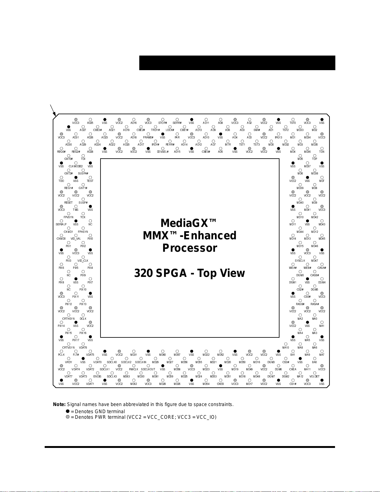
Pin Assignments
g
Index Corner
1234567891011121314151617181920
A
B
C
D
E
F
G
H
J
K
L
M
N
P
Q
R
S
T
U
V
W
X
Y
Z
AA
AB
AC
AD
AE
AF
AG
AH
AJ
AK
AL
AM
AN
9&& $' 966 9&& $' 9&& 6723 6(55 966 $' $' 9&& $' 9&& 966 767 9&& 966
966 $' &%( $' $' &%( 75'< /2&. &%( $' $' $' $' 60, $' 767 0' 0'
9&& $' $' $' 9&& $' )5$0( 966 3$5 9&& $' 966 $' $' 9&& ,54 0' 0' 9&&
$' $' $' $' $' $' ,5'< 3(55 $' $' $' ,175 767 767 0' 0' 0' 0'
5(4 5(4 $' 966 9&& 9&& 966 '(96(/ $' 966 &%( $' 966 9&& 9&& 966 0' 0' 7'1
*17 7', 0' 7'3
966 &/.02'( 966 966 0' 966
*17 6863$
7'2 966 7(67
5(4 *17
9&& 9&& 9&&
5(6(7 6863
9&& 706 966
)396<1 7&.
6(5,$/3 966 1&
&.0' )3+6<1
&.0' 9,'B9$/ 3,;
3,; 3,;
966 9&& 966
3,; 9,'B&/.
3,; 3,; 3,;
1& 3,;
3,; 966 3,;
1& 3,;
9&& 3,; 966
3,; 3,;
9&& 9&& 9&&
&57+6<1 '&/.
3,; 966 9&&
3,; 3,;
966 3,; 966
&5796<1 9'$7
3&/. )/7 9'$7 966 9&& 0' 966 0' 0' 966 0' 0' 966 9&& 9&& 966 %$ 0$ 0$
95'< 966 9'$7 6'&/. 6'&/. 6'&/.,1 0' 0' 0' 0' 0' 0' 0' 0' '40 &6
9&& 9'$7 9'$7 6'&/. 9&& 5:&/. 6'&/.287 966 0' 9&& 0' 966 0' 0' 9&& '40 &.($ 0$ 9&&
9'$7 9'$7 (1',6 6'&/. 0' 0' 0' 0' 0' 0' 0' 0' 0' 0' '40 '40 0$ 92/'(7
966 9&& 9'$7 966 9&& 0' 9&& 0' 0' 966 0' &.(% 9&& 0' 9&& 966 &6 9&& 966
1234567891011121314151617181920
320 SPGA - Top View
MediaGX™
MMX™-Enhanced
Processor
21 22 23 24 25 26
21 22 23 24 25 26 27 28 29 30 31 32 33 34 35 36 37
27 28 29 30 31 32 33 34 35 36 37
9&& 966 0'
9&& 9&& 9&&
966 0' 9&&
0' 966 0'
0' 0' 0'
966 9&& 966
:($ :(% &$6$
'40 966 '40
966 &6 9&&
9&& 9&& 9&&
9&& 966 0$
966 0$ 966
0' 0'
0' 0'
0' 0'
0' 0'
0' 0'
0' 0'
6<6&/. 0'
'40 &$6%
&6 '40
5$6% 5$6$
0$ 0$
0$ 0$
0$ 0$0$
966 %$
A
B
C
D
E
F
G
H
J
K
L
M
N
P
Q
R
S
T
U
V
W
X
Y
Z
AA
AB
AC
AD
AE
AF
AG
AH
AJ
AK
AL
AM
AN
Note: Si
nal names have been abbreviated in this figure due to space constraints.
= Denotes GND terminal
= Denotes PWR terminal (VCC2 = VCC_CORE; VCC3 = VCC_IO)
Figure 2-3 320 SPGA Pin Assignment Diagram
Page 16 Cyrix Corporation Confidential GXm_db_v2.0
Page 33
Table 2-4 320 SPGA Pin Assignments - Sorted by Pin Number
Pin
No. Signal Name
A3 VCC3
A5 AD25
A7 VSS
A9 VCC2
A11 AD16
A13 VCC3
A15 STOP#
A17 SERR#
A19 VSS
A21 AD11
A23 AD8
A25 VCC3
A27 AD2
A29 VCC2
A31 VSS
A33 TEST0
A35 VCC3
A37 VSS
B2 VSS
B4 AD27
B6 C/BE3#
B8 AD21
B10 AD19
B12 C/BE2#
B14 TRDY#
B16 LOCK#
B18 C/BE1#
B20 AD13
B22 AD9
B24 AD6
B26 AD3
B28 SMI#
B30 AD1
B32 TEST2
B34 MD33
B36 MD2
C1 VCC3
C3 AD31
C5 AD26
C7 AD23
Pin
No. Signal Name
C9 VCC2
C11 AD18
C13 FRAME#
C15 VSS
C17 PAR
C19 VCC3
C21 AD10
C23 VSS
C25 AD4
C27 AD0
C29 VCC2
C31 IRQ13
C33 MD1
C35 MD34
C37 VCC3
D2 AD30
D4 AD29
D6 AD24
D8 AD22
D10 AD20
D12 AD17
D14 IRDY#
D16 PERR#
D18 AD14
D20 AD12
D22 AD7
D24 INTR
D26 TEST1
D28 TEST3
D30 MD0
D32 MD32
D34 MD3
D36 MD35
E1 REQ0#
E3 REQ2#
E5 AD28
E7 VSS
E9 VCC2
E11 VCC2
E13 VSS
Pin
No. Signal Name
E15 DEVSEL#
E17 AD15
E19 VSS
E21 C/BE0#
E23 AD5
E25 VSS
E27 VCC2
E29 VCC2
E31 VSS
E33 MD4
E35 MD36
E37 TDN
F2 GNT0#
F4 TDI
F34 MD5
F36 TDP
G1 VSS
G3 CLKMODE2
G5 VSS
G33 VSS
G35 MD37
G37 VSS
H2 GNT2#
H4 SUSPA#
H34 MD6
H36 MD38
J1 TDO
J3 VSS
J5 TEST
J33 VCC2
J35 VSS
J37 MD7
K2 REQ1#
K4 GNT1#
K34 MD39
K36 MD8
L1 VCC2
L3 VCC2
L5 VCC2
L33 VCC2
Pin Assignments
Pin
No. Signal Name
L35 VCC2
L37 VCC2
M2 RESET
M4 SUSP#
M34 MD40
M36 MD9
N1 VCC3
N3 TMS
N5 VSS
N33 VSS
N35 MD41
N37 VCC3
P2 FP_VSYNC
P4 TCLK
P34 MD10
P36 MD42
Q1 SERIALP
Q3 VSS
Q5 NC
Q33 MD11
Q35 VSS
Q37 MD43
R2 CLKMODE1
R4 FP_HSYNC
R34 MD44
R36 MD12
S1 CLKMODE0
S3 VID_VAL
S5 PIXEL0
S33 MD14
S35 MD13
S37 MD45
T2 PIXEL1
T4 PIXEL2
T34 MD15
T36 MD46
U1 VSS
U3 VCC3
U5 VSS
U33 VSS
2
Pin
No. Signal Name
U35 VCC3
U37 VSS
V2 PIXEL3
V4 VID_CLK
V34 SYSCLK
V36 MD47
W1 PIXEL6
W3 PIXEL5
W5 PIXEL4
W33 WEA#
W35 WEB#
W37 CASA#
X2 NC
X4 PIXEL9
X34 DQM0
X36 CASB#
Y1 PIXEL8
Y3 VSS
Y5 PIXEL7
Y33 DQM1
Y35 VSS
Y37 DQM4
Z2 NC
Z4 PIXEL10
Z34 CS2#
Z36 DQM5
AA1 VCC3
AA3 PIXEL11
AA5 VSS
AA33 VSS
AA35 CS0#
AA37 VCC3
AB2 PIXEL12
AB4 PIXEL13
AB34 RASB#
AB36 RASA#
AC1 VCC2
AC3 VCC2
AC5 VCC2
AC33 VCC2
GXm_db_v2.0 Cyrix Corporation Confidential Page 17
Page 34
Pin Assignments
Table 2-4 320 SPGA Pin Assignments - Sorted by Pin Number (cont.)
Pin
No. Signal Name
AC35 VCC2
AC37 VCC2
AD2 CRT_HSYNC
AD4 DCLK
AD34 MA2
AD36 MA0
AE1 PIXEL14
AE3 VSS
AE5 VCC2
AE33 VCC2
AE35 VSS
AE37 MA1
AF2 PIXEL15
AF4 PIXEL16
AF34 MA4
AF36 MA3
AG1 VSS
AG3 PIXEL17
AG5 VSS
AG33 VSS
AG35 MA5
AG37 VSS
AH2 CRT_VSYNC
AH4 VID_DATA6
AH32 MA10
AH34 MA8
AH36 MA6
AJ1 PCLK
Pin
No. Signal Name
AJ3 FTL#
AJ5 VID_DATA5
AJ7 VSS
AJ9 VCC2
AJ11 MD31
AJ13 VSS
AJ15 MD60
AJ17 MD57
AJ19 VSS
AJ21 MD22
AJ23 MD52
AJ25 VSS
AJ27 VCC2
AJ29 VCC2
AJ31 VSS
AJ33 BA1
AJ35 MA9
AJ37 MA7
AK2 VID_RDY
AK4 VSS
AK6 VID_DATA0
AK8 SDCLK0
AK10 SDCLK2
AK12 SDCLK_IN
AK14 MD29
AK16 MD27
AK18 MD56
AK20 MD55
Pin
No. Signal Name
AK22 MD21
AK24 MD20
AK26 MD50
AK28 MD16
AK30 DQM3
AK32 CS3#
AK34 VSS
AK36 BA0
AL1 VCC2
AL3 VID_DATA4
AL5 VID_DATA2
AL7 SDCLK1
AL9 VCC2
AL11 RW_CLK
AL13 SDCLK_OUT
AL15 VSS
AL17 MD58
AL19 VCC3
AL21 MD23
AL23 VSS
AL25 MD19
AL27 MD49
AL29 VCC2
AL31 DQM6
AL33 CKEA
AL35 MA11
AL37 VCC3
AM2 VID_DATA7
Pin
No. Signal Name
AM4 VID_DATA3
AM6 ENA_DISP
AM8 SDCLK3
AM10 MD63
AM12 MD30
AM14 MD61
AM16 MD59
AM18 MD25
AM20 MD24
AM22 MD53
AM24 MD51
AM26 MD18
AM28 MD48
AM30 DQM7
AM32 DQM2
AM34 MA12
AM36 VOLDET
AN1 VSS
AN3 VCC2
AN5 VID_DATA1
AN7 VSS
AN9 VCC2
AN11 MD62
AN13 VCC3
AN15 MD28
AN17 MD26
AN19 VSS
AN21 MD54
Pin
No. Signal Name
AN23 CKEB
AN25 VCC3
AN27 MD17
AN29 VCC2
AN31 VSS
AN33 CS1#
AN35 VCC3
AN37 VSS
Page 18 Cyrix Corporation Confidential GXm_db_v2.0
Page 35
Pin Assignments
Table 2-5 320 SPGA Pin Assignments - Sorted Alphabetically by Signal Name
Signal Name Type P in . No .
AD0 I/O C27
AD1 I/O B30
AD2 I/O A27
AD3 I/O B26
AD4 I/O C25
AD5 I/O E23
AD6 I/O B24
AD7 I/O D22
AD8 I/O A23
AD9 I/O B22
AD10 I/O C21
AD11 I/O A21
AD12 I/O D20
AD13 I/O B20
AD14 I/O D18
AD15 I/O E17
AD16 I/O A11
AD17 I/O D12
AD18 I/O C11
AD19 I/O B10
AD20 I/O D10
AD21 I/O B8
AD22 I/O D8
AD23 I/O C7
AD24 I/O D6
AD25 I/O A5
AD26 I/O C5
AD27 I/O B4
AD28 I/O E5
AD29 I/O D4
AD30 I/O D2
AD31 I/O C3
BA0 O AK3 6
BA1 O AJ33
CASA# O W37
CASB# O X36
C/BE0# I/O E21
C/BE1# I/O B18
C/BE2# I/O B12
C/BE3# I/O B6
CKEA O AL33
CKEB O AN23
CLKMODE0 I S1
CLKMODE1 I R2
CLKMODE2 I G3
Signal Name Type Pin. No.
CRT_HSYNC O AD2
CRT_VSYNC O AH2
CS0# O AA35
CS1# O AN33
CS2# O Z34
CS3# O AK32
DCLK I AD4
DEVSEL# s/t/s E15 (PU)
DQM0 O X34
DQM1 O Y33
DQM2 O AM32
DQM3 O AK30
DQM4 O Y37
DQM5 O Z36
DQM6 O AL31
DQM7 O AM30
ENA_DISP O AM6
FLT# I AJ3
FP_HSYNC O R4
FP_VSYNC O P2
FRAME# s/t/s C13 (PU)
GNT0# O F2
GNT1# O K4
GNT2# O H2
INTR I D24
IRDY# s/t/s D14 (PU)
IRQ13 O C31
LOCK# s/t/s B16 (PU)
MA0 O AD36
MA1 O AE37
MA2 O AD34
MA3 O AF36
MA4 O AF34
MA5 O AG35
MA6 O AH36
MA7 O AJ37
MA8 O AH34
MA9 O AJ35
MA10 O AH32
MA11 O AL35
MA12 O AM34
MD0 I/O D30
MD1 I/O C33
MD2 I/O B36
MD3 I/O D34
Signal Name Type Pin. No.
MD4 I/O E33
MD5 I/O F34
MD6 I/O H34
MD7 I/O J37
MD8 I/O K36
MD9 I/O M36
MD10 I/O P34
MD11 I/O Q33
MD12 I/O R36
MD13 I/O S35
MD14 I/O S33
MD15 I/O T34
MD16 I/O A K28
MD17 I/O AN27
MD18 I/O AM26
MD19 I/O AL25
MD20 I/O A K24
MD21 I/O A K22
MD22 I/O AJ21
MD23 I/O AL21
MD24 I/O AM20
MD25 I/O AM18
MD26 I/O AN17
MD27 I/O A K16
MD28 I/O AN15
MD29 I/O A K14
MD30 I/O AM12
MD31 I/O AJ 11
MD32 I/O D32
MD33 I/O B34
MD34 I/O C35
MD35 I/O D36
MD36 I/O E35
MD37 I/O G35
MD38 I/O H36
MD39 I/O K34
MD40 I/O M34
MD41 I/O N35
MD42 I/O P36
MD43 I/O Q37
MD44 I/O R34
MD45 I/O S37
MD46 I/O T36
MD47 I/O V36
MD48 I/O AM28
Signal Name Type Pin. No.
MD49 I/O AL27
MD50 I/O AK26
MD51 I/O AM24
MD52 I/O AJ23
MD53 I/O AM22
MD54 I/O AN21
MD55 I/O AK20
MD56 I/O AK18
MD57 I/O AJ17
MD58 I/O AL17
MD59 I/O AM16
MD60 I/O AJ15
MD61 I/O AM14
MD62 I/O AN11
MD63 I/O AM10
NC Q5
NC X2
NC Z2
PAR I/O C17
PCLK O AJ1
PERR# s/t/s D16 (PU)
PIXEL0 O S5
PIXEL1 O T2
PIXEL2 O T4
PIXEL3 O V2
PIXEL4 O W5
PIXEL5 O W3
PIXEL6 O W1
PIXEL7 O Y5
PIXEL8 O Y1
PIXEL9 O X4
PIXEL10 O Z4
PIXEL11 O AA3
PIXEL12 O AB2
PIXEL13 O AB4
PIXEL14 O AE1
PIXEL15 O AF2
PIXEL16 O AF4
PIXEL17 O AG3
RASA# O AB36
RASB# O AB34
REQ0# I E1 (PU)
REQ1# I K2 (PU)
REQ2# I E3 (PU)
RESET I M2
2
GXm_db_v2.0 Cyrix Corporation Confidential Page 19
Page 36
Pin Assignments
Table 2-5 320 SPGA Pin Assignments - Sorted Alphabetically by Signal Name (cont.)
Signal Name Type P in . No .
RW_CLK O AL11
SDCLK_IN I AK12
SDCLK_OUT O AL13
SDCLK0 O AK8
SDCLK1 O AL7
SDCLK2 O AK10
SDCLK3 O AM8
SERIALP O Q1
SERR# OD A17 (PU)
SMI# I B28
STOP# s/t/s A15 (PU)
SUSP# I M4 (PU)
SUSPA# O H4
SYSCLK I V34
TCLK I P4 (PU)
TDI I F4 (PU)
TDN O E37
TDO O J1
TDP O F36
TEST I J5 (PD)
TEST0 O A33
TEST1 O D26
TEST2 O B32
TEST3 O D28
TMS I N3 (PU)
TRDY# s/t/s B14 (PU)
VCC2 PWR A9
VCC2 PWR A29
VCC2 PWR C9
VCC2 PWR C29
VCC2 PWR E9
VCC2 PWR E11
VCC2 PWR E27
VCC2 PWR E29
VCC2 PWR J33
VCC2 PWR L1
VCC2 PWR L3
VCC2 PWR L5
VCC2 PWR L33
VCC2 PWR L35
VCC2 PWR L37
VCC2 PWR AC1
VCC2 PWR AC3
VCC2 PWR AC5
Signal Name Type Pin. No.
VCC2 PWR AC33
VCC2 PWR AC35
VCC2 PWR AC37
VCC2 PWR AE5
VCC2 PWR AE33
VCC2 PWR AJ9
VCC2 PWR AJ27
VCC2 PWR AJ29
VCC2 PWR AL1
VCC2 PWR AL9
VCC2 PWR AL29
VCC2 PWR AN3
VCC2 PWR AN9
VCC2 PWR AN29
VCC3 PWR A3
VCC3 PWR A13
VCC3 PWR A25
VCC3 PWR A35
VCC3 PWR C1
VCC3 PWR C19
VCC3 PWR C37
VCC3 PWR N1
VCC3 PWR N37
VCC3 PWR U3
VCC3 PWR U35
VCC3 PWR AA1
VCC3 PWR AA37
VCC3 PWR AL19
VCC3 PWR AL37
VCC3 PWR AN13
VCC3 PWR AN25
VCC3 PWR AN35
VID_CLK O V4
VID_DATA0 O AK6
VID_DATA1 O AN5
VID_DATA2 O AL5
VID_DATA3 O AM4
VID_DATA4 O AL3
VID_DATA5 O AJ5
VID_DATA6 O AH4
VID_DATA7 O AM2
VID_RDY I AK2
VID_VAL O S3
VOLDET O AM36
Signal Name Type Pin. No.
VSS GND A7
VSS GND A19
VSS GND A31
VSS GND A37
VSS GND B2
VSS GND C15
VSS GND C23
VSS GND E7
VSS GND E13
VSS GND E19
VSS GND E25
VSS GND E31
VSS GND G 1
VSS GND G 5
VSS GND G33
VSS GND G37
VSS GND J3
VSS GND J35
VSS GND N5
VSS GND N33
VSS GND Q 3
VSS GND Q35
VSS GND U1
VSS GND U5
VSS GND U33
VSS GND U37
VSS GND Y3
VSS GND Y35
VSS GND AA5
VSS GND AA33
VSS GND AE3
VSS GND AE35
VSS GND AG1
VSS GND AG5
VSS GND AG33
VSS GND AG37
VSS GND AJ7
VSS GND AJ13
VSS GND AJ19
VSS GND AJ25
VSS GND AJ31
VSS GND AK4
VSS GND AK34
VSS GND AL15
Signal Name Type Pin. No.
VSS GND AL23
VSS GND AN1
VSS GND AN7
VSS GND AN19
VSS GND AN31
VSS GND AN37
WEA# O W33
WEB# O W35
Note:
PU/PD indicates pin is
internally connected to
a 20-kohm pull-up/
down resistor
Page 20 Cyrix Corporation Confidential GXm_db_v2.0
Page 37
2.2 Signal Descriptions
2.2.1 System Interface Signals
Signal Descriptions
2
BGA
Signal Name
SYSCLK P26 V34 I System Clock
CLKMODE[2 :0] M1, L1, M3G3, R2,
Pin No.
SPGA
Pin No. Type Description
System Clock runs synchronously with the PCI bus. The internal clock of the M edi aG X p r oc es sor is g enerated by an int erna l
PLL which multiplies the SYSCLK input and can run up to eight
times faster . The SYSCLK to core clock multiplier is con fig ured
using the CLKMOD[2:0] inputs.
The SYSCLK input is a fixed frequency which can only be
stopped or varied when the MediaGX processor is in a full 3V
Suspend. (Section 6.4 “3-Volt Suspend Mode” on page 203 for
details regarding this mode.)
I Clock Mode
S1
These signals are u sed to set th e core c lock multi plier. The PCI
clock "SYSCLK" is multiplied by the value programmed by
CLKMODE[2:0] to generate the MediaGX processor’s core
clock. CLKMODE2 is valid only for MediaGX MMX-Enhanced
processor revision 4.0 and up. The value read from DIR1
(Device ID Register 1, refer to page 56) affects the definition of
the CLKMOD E pins.
If DIR1 = 30h -33h then CLK M ODE[1:0]:
00 = SYSCLK multiplied by 4 (Test mode only)
01 = SYSCLK multiplied by 6
10 = SYSCLK multiplied by 7
11 = SYSCLK multiplied by 5
If DIR1 = 34h-4Fh then CLKMODE[1:0]:
00 = SYSCLK multiplied by 4 (Test mode only)
01 = SYSCLK multiplied by 6
10 = SYSCLK multiplied by 7
11 = SYSCLK multiplied by 8
If DIR1 > or = 50h then CLKMODE[2:0]:
000 = SYSCLK multiplied by 4 (Test mode only)
001 = SYSCLK multiplied by 10
010 = SYSCLK multiplied by 9
01 1 = SYSCLK multi pli ed by 5
100 = SYSCLK multiplied by 4
101 = SYSCLK multiplied by 6
1 10 = SYSCLK multi pli ed by 7
111 = SYSCLK multiplied by 8
GXm_db_v2.0 Cyrix Corporation Confidential Page 21
Page 38
Signal Descriptions
2.2.1 System Interface Signals (cont.)
BGA
Signal Name
RESET J3 M2 I Reset
INTR B18 D24 I (Maskable) Interrupt Request
IRQ13 C22 C31 O Interrupt Request Level 13
Pin No.
SPGA
Pin No. Type Description
RESET aborts all operations in progress and places the
MediaGX processor into a reset state. RESET forces the CPU
and peripheral functions to begin executing at a known state.
All data in the on-chip cache is invalidated.
RESET is an asynchronous input but must meet specified
setup and hold times to guarantee recognition at a particular
clock edge. This input is typically generated during the PowerOn-Reset sequence.
Note: Warm Reset does not re qui re a n in put o n the Me dia GX
processor since the function is virtualized using SMM.
INTR is a level-sensitive input that causes the MediaGX processor to Suspend execution of the current instruction stream
and begin execution of an interrupt service routine. The INTR
input can be masked through the Flags Register IF bit. (See
Table 3-4 "EFLAGS Register" on page 45 for bit definitions.)
IRQ13 is asserted if an on-chip floating point error occurs.
When a floating point error occurs, the MediaGX processor
asserts the IRQ13 pin. The floating point interrupt handler then
performs an OUT instruction to I/O address F0h or F1h. The
MediaGX processor accepts either of these cycles and clears
the IRQ13 pin.
Refer to Section 3.4.1 “I/O Address Space” on page 65 for further information on IN/OUT instructions.
SMI# C19 B28 I System Management Interrupt
SMI# is a level-sensitive interrupt. SMI# puts the MediaGX processor into System Management Mode (SMM).
Page 22 Cyrix Corporation Confidential GXm_db_v2.0
Page 39
2.2.1 System Interface Signals (cont.)
Signal Descriptions
2
BGA
Signal Name
SUSP# H2
SUSPA# E2 H4 O Suspend Acknowledge
Pin No.
(PU)
SPGA
Pin No. Type Description
M4
(PU)
I Suspend Request
This signal is used to request that the MediaGX processor
enter Suspend mode. After recognition of an active SUSP#
input, the processor completes execution of the current instruction, any pending decoded instructions and associated bus
cycles. SUSP# is ignored following RESET# and is enabled by
setting the SUSP bit in CCR2. (See Table 3-11 "Configuration
Registers" on page 52 for CCR2 bit definitions.)
Since the MediaGX processor includes s y stem logic functions
as well as the CPU core, there are special modes designed to
support the differe nt power manag ement states as sociated with
APM, ACPI, and portable designs. The part can be configured
to stop only the CPU core clocks, or all clocks. When all clocks
are stopped, the external clock can also be stopped. (See Section 6 “Power Management” on page 201 for more details
regarding power management states.)
This pin is internally connected to a 20-kohm pull-up resistor.
SUSP# is pulled up when not active.
Suspend Acknowledge indicates that the MediaGX processor
has entered low-power Suspend mode as a result of SUSP#
assertion or executi on of a HALT instruction. SUSP A# floats following RESET# and is enabled by setting the SUSP bit in
CCR2. (See Table 3-11 "Configuration Registers" on page 52
for CCR2 bit definitions.)
The SYSCLK input may be stopped after SUSPA# has been
asserted to further reduce power consumption if the system is
configured for 3V Suspend mode . (Sectio n 6.4 “3-Volt Suspend
Mode” on page 203 for details regarding this mode.)
SERIALP L3 Q1 O Serial Packet
Serial Packet is the s ing le wire s erial-tra ns mi ssion s ig nal to th e
Cx5520 chip. The clock used for this interface is the PCI clock
(SYSCLK). This interface carries packets of miscellaneous
information to the chipset to be used by the VSA software handlers.
GXm_db_v2.0 Cyrix Corporation Confidential Page 23
Page 40
Signal Descriptions
2.2.2 PCI Interface Signals
BGA
Signal Name
AD[31:0] Refer
C/BE[3:0]# D5,
Pin No.
to T able
2-3
B8,
C13,
A15
SPGA
Pin No Type Description
Refer
to T able
2-5
B6, B12,
B18,
E21
I/O Multiplexed Address and Data
Addresses and data are multiplexed on the same PCI pins. A
bus transaction consists of an address phase in the cycle in
which FRAME# is asserted followed by one or more data
phases. During the ad dress phase , AD[3 1:0] co ntain a phys ical
32-bit address. For I/O, this is a byte address, for configuration
and memory it is a DWORD address. During data phases,
AD[7:0] contain the least significant byte (LSB) and AD[31:24]
contain the most significant byte (MSB). Write data is stable
and valid when IRDY# is asserted and read data is stable and
valid when TRDY# is asserted. Data is transferred during those
SYSCLKS where both IRDY# and TRDY# are asserted.
I/O Multiplexed Command and Byte Enables
Bus command and byte enables are multiplexed on the same
PCI pins. During the address phase of a transaction when
FRAME# is active, C/BE[3:0]# define the bu s command. Durin g
the data phase C/BE[3:0]# are used as byte enables. The byte
enables are val id for t he entire data p hase an d deter mine whi ch
byte lanes carry meaningful data. C/BE0# applies to byte 0
(LSB) and C/BE3# applies to byte 3 (MSB).
The command encoding and types are listed below.
0000 = Interrupt Acknowledge
0001 = Special Cycle
0010 = I/O Read
0011 = I/O Write
0100 = Reserved
0101 = Reserved
0110 = Memory Read
0111 = Memory Write
1000 = Reserved
1001 = Reserved
1010 = Configuration Read
1011 = Configuration Write
1100 = Memory Read Multiple
1101 = Dual Address Cycle (Reserved)
1 110 = Memory Read Line
1111 = Memory Write and Invalidate
Page 24 Cyrix Corporation Confidential GXm_db_v2.0
Page 41
2.2.2 PCI Interface Signals (cont.)
Signal Descriptions
2
BGA
Signal Name
PAR B12 C17 I/O Parity
FRAME# A8
IRDY# C9
TRDY# B9
Pin No.
(PU)
(PU)
(PU)
SPGA
Pin No Type Description
Parity generation is required by all PCI agents: the master
drives P AR for a ddress and w rite-data ph ases, the target drive s
PAR for read-data phases. Parity is even across AD[31:0] and
C/BE[3:0]#.
For address phases, PAR is stable and valid one SYSCLK after
the address phase. It has the same timing as AD[31:0] but
delayed by one SYSCLK.
For data phases, PAR is stable and valid one SYSCLK after
either IRDY# is asserted on a write transaction or after TRDY#
is asserted on a read transaction. Once PAR is valid, it remains
valid until one SYSCLK after the completion of the data phase.
(Also see PERR#.)
C13
(PU)
D14
(PU)
B14
(PU)
s/t/s Frame
Cycle Frame is driven by the current master to indicate the
beginning and duration of an access. FRAME# is asserted to
indicate a bus transaction is beginning. While FRAME# is
asserted, data transfers continue. When FRAME# is deasserted, the transaction is in the final data phase.
This pin is internally connected to a 20-kohm pull-up resistor.
s/t/s Initiator Ready
Initiator Ready is asserted to indicate that the bus master is
able to complete the current data phase of the transaction.
IRDY# is used in conjunction with TRDY#. A data phase is
completed on any SYSCLK in which both IRDY# and TRDY#
are sampled asserted. During a write, IRDY# indicates valid
data is present on AD[31:0]. During a read, it in dicat es the ma ster is prepared to accept data. Wait cycles are inserted until
both IRDY# and TRDY# are asserted together.
This pin is internally connected to a 20-kohm pull-up resistor.
s/t/s Target Ready
TRDY# is asserted to indicate that the target agent is able to
complete the current data phase of the transaction. TRDY# is
used in conjunction with IRDY#. A data phase is complete on
any SYSCLK in which both TRDY# and IRDY# are sampled
asserted. During a read, TRDY# indicates that valid data is
present on AD[31:0]. During a write, it indicates the target is
prepared to accept data. Wait cycles are inserted until both
IRDY# and TRDY# are asserted together.
This pin is internally connected to a 20-kohm pull-up resistor.
GXm_db_v2.0 Cyrix Corporation Confidential Page 25
Page 42
Signal Descriptions
2.2.2 PCI Interface Signals (cont.)
BGA
Signal Name
STOP# C11
LOCK# B11
DEVSEL# A9
Pin No.
(PU)
(PU)
(PU)
SPGA
Pin No Type Description
A15
(PU)
B16
(PU)
E15
(PU)
s/t/s Target Stop
STOP# is asserted to indicate that the current target is requesting the master to stop the current transaction. This signal is
used with DEVSEL# to indicate retry, disconnect or target
abort. If STOP# is sam ple d a cti ve whi le a m ast er, FRAME# will
be deasserted and the cycle stopped within three SYSCLK
cycles. As an input, STOP# can be asserted in the following
cases. 1) If a PCI master tries to acce ss memory that has bee n
locked by another mast er . This conditi on is detected if FRAME#
and LOCK# are asserted during an addr es s phas e. 2) ST O P#
will also be asserted if the PCI write buffers are full or if a previously buffered cycle has not completed. 3) Finally, STOP# can
be asserted on read cycles that cross cache line boundaries.
This is conditional based upon the programming of bit 1 in PCI
Control Function 2 Register. (See Table 4-38 "PCI Configuration Registers" on page 179 for programming details.)
This pin is internally connected to a 20-kohm pull-up resistor.
s/t/s Lock Operation
LOCK# indicates an ato mi c o peration that may re qui re m ul tip le
transactions to complete. When LOCK# is asserted, nonexclusive transactions may pr oceed to an address that is not currently locked (at least 16 bytes must be locked). A grant to start
a transaction on PCI does not guarantee control of LOCK#.
Control of LOCK# is obtained under it own protocol in conjunction with GNT#. It is possible for different agents to use PCI
while a single master retains ownership of LOCK#. The arbiter
can implement a co mp lete system lock. In this mode, if LOCK#
is active, no other master can gain access to the system until
the LOCK# is deasserted.
This pin is internally connected to a 20-kohm pull-up resistor.
s/t/s Device Select
DEVSEL# indicates that the driving device has decoded its
address as the target of the current access. As an input,
DEVSEL# indicates whether any device on the bus has been
selected. DEVSEL# will also be driven by any agent that has
the ability to accept cycles on a subtractive decode basis. As a
master, if no DEVSEL# is detec ted within and up to the subtra ctive decode clock, a master abort cycle will result expect for
special cycles which do not expect a DEVSEL# returned.
This pin is internally connected to a 20-kohm pull-up resistor.
Page 26 Cyrix Corporation Confidential GXm_db_v2.0
Page 43
2.2.2 PCI Interface Signals (cont.)
Signal Descriptions
2
BGA
Signal Name
PERR# A11
SERR# C12
REQ[2:0]# D3,
Pin No.
(PU)
(PU)
H3,
E3
(PU)
SPGA
Pin No Type Description
D16
(PU)
A17
(PU)
E3,
K2,
E1
(PU)
s/t/s Parity Error
PERR# is used for repor ting of data parity errors during all PCI
transactions except a Special Cycle. The PERR# line is driven
two SYSCLKs after the data in which the error was detected.
This is one SYSCLK after the PAR that is attached to the data.
The minimum duration of PE RR# is one SYSCLK for eac h data
phase in which a data parity error is detected. PERR# must be
driven high for one SYSCLK before being tristated. A target
asserts PERR# on write cycles if it has claimed the cycle with
DEVSEL#. The master asserts PERR# on read cycles.
This pin is internally connected to a 20-kohm pull-up resistor.
OD System Error
System Error may be asserted by any ag ent for reporting er rors
other than PCI parity. The intent is to have the PCI central
agent assert NMI to the processor. When the Parity Enable bit
is set in the Memory Controller Configuration register, SERR#
will be asserted upon detecting a parity error on read operations from DRAM.
I Request Lines
Request indicates t o the arbite r that an agen t desires use of the
bus. Each master has its own REQ# line. REQ# priorities are
based on the arbitration scheme chosen.
Each of these pins are internally connected to a 20-kohm pullup resistor.
GNT[2:0]# E1,
F2,
D1
GXm_db_v2.0 Cyrix Corporation Confidential Page 27
H2,
K4,
F2
O Grant Lines
Grant indicates to the requesting master that it has been
granted access to the bu s. Ea ch ma ster has its ow n GNT# line.
GNT# can be pulled away at any time a higher REQ# is
received or if the master does not begin a cycle within a minimum period of time (16 SYSCLKs).
Page 44
Signal Descriptions
2.2.3 Memory Controller Interface Signals
BGA
Signal Name
Note: The memory controller interface supports two types of memory configurations: SDRAM modules on the sys-
tem board and JEDEC DIMM c onn ectors. Refer to Section 4.3 “M em ory C o ntro lle r” on p age 116 for detailed
information regarding signal connections.
MD[63:0] Refer
MA[12:0] Refer
BA[1:0] AD26,
CS[3:0]# AE23,
RASA#,
RASB#
CASA#,
CASB#
WEA#,
WEB#
Pin No.
to T able
2-3
to T able
2-3
AD25
V25,
AD23,
V26
W24,
W25
P25,
R26
R25,
R24
SPGA
Pin No. Type Description
Refer
to T able
2-5
Refer
to T able
2-5
AJ33,
AK36
AK32,
Z34,
AN33,
AA35
AB36,
AB34
W37,
X36
W33,
W35
I/O Memory Data Bus
The data bus lines driven to/from system memory.
O Memory Address Bus
The multiplexed ro w/column address li ne s driven to the s ys tem
memory.
Supports 256Mbit SDRAM.
O Bank Address Bits
These bits are used to select the component bank within the
SDRAM.
O Chip Selects
The chip selects are used to select the module bank within the
system memory. Each chip select corresponds to a specific
module bank.
If CS# is high, the bank(s) do not respond to RAS#, CAS#,
WE# until the bank is selected again.
O Row Address Strobe
RAS#, CAS#, WE# and CKE are encoded to support the different SDRAM commands. RASA# is used with CS[1: 0]# . RASB#
is used with CS[3:2]#.
O Column Address Strobe
RAS#, CAS#, WE# and CKE are encoded to support the different SDRAM commands. CASA# is used with CS[1: 0]# . CASB#
is used with CS[3:2]#.
O Write Enable
RAS#, CAS#, WE# and CKE are encoded to support the different SDRAM commands. WEA# is used with CS[1:0]#. WEB# is
used with CS[3:2]#.
Page 28 Cyrix Corporation Confidential GXm_db_v2.0
Page 45
2.2.3 Memory Controller Interface Signals (cont.)
Signal Descriptions
2
BGA
Signal Name
DQM[7:0] Refer
CKEA,
CKEB
SDCLK[3:0] AE4,
SDCLK_IN AE8 AK12 I SDRAM Clock Input
SDCLK_OUT AF8 AL13 O SDRAM Clock Output
Pin No.
to T able
2-3
AF24,
AD16
AF5,
AE5,
AF4
SPGA
Pin No. Type Description
Refer
to T able
2-5
AL33,
AN23
AM8,
AK10,
AL7,
AK8
O Data Mask Control Bits
During memory read cycles, these outputs control whether the
SDRAM output buffers are driven on the MD bus or not. All
DQM signals are asserted during read cycles.
During memory write cycles, these outputs control whether or
not MD data will be written into the SDRAM.
DQM[7:0] connect directly to the DQM7-0 pins of each connector.
O Clock Enable
These signals are used to enter Suspend/power-down mode.
When CKE goes low when no read or write cycle is in progress,
the SDRAM enters power-down mode. To ensure that SDRAM
data remains valid, the self-refresh command is executed. To
exit this mode, drive CKE high.
For normal operation, CKE should be held high.
O SDRAM Clocks
The SDRAM samples all the control, address, and data using
these clocks. SDCLK[3:0] should be used with CS[3:0]#,
respectively, for the Suspend mode to function correctly.
The MediaGX proces sor sam ples the memo ry read d ata on t his
clock. Works in conjunction with the SDCLK_OUT signal.
This output is routed back to SDCLK_IN. The board designer
should vary the length of the board trace to control skew
between SDCLK_IN and SDCLK.
GXm_db_v2.0 Cyrix Corporation Confidential Page 29
Page 46
Signal Descriptions
2.2.4 Video Interface Signals
BGA
Signal Name
PCLK AC1 AJ1 O Pixel Port Clock
VID_CLK P1 V4 O Video Clock
DCLK AB1 AD4 I Dotclock
CRT_HSYNC W2 AD2 O CRT Horizontal Sync
CRT_VSYNC AA3 AH2 O CRT Vertical Sync
FP_HSYNC L2 R4 O Flat Panel Horizontal Sync
Pin No
SPGA
Pin No Type Description
Pixel Port Clock rep resents t he pixel dotcloc k or a 2x multipl e of
the dotclock for some 16-bit-per-pixel modes. It determines the
data transfer rate from the MediaGX processor to the
Cx5520/Cx5530.
Video Clock represents the video port clock to the
Cx5520/Cx5530. This pin is only used if the Video Port is
enabled.
The DCLK input is driven from the Cx5520/Cx5530 and represents the pixel dot cloc k. In some cases, such as when displaying 16 BPP data with an eight-bit-graphics pixel port, this clock
will actually be a 2x multiple of th e dotclock.
CRT Horizontal Sync establishes the line rate and horizontal
retrace interval for an attached C RT. The polarity is programmable and depends on the display mode.
CRT V ertic al Sync es tablis hes th e screen re fresh rat e and vertical retrace interval for an attached CRT. The polarity is programmable and depends on the dis play mode.
Flat Panel Horizontal Sync establishes the line rate and horizontal retrace interval for a TFT display. Polarity is programmable and depends on the display mode.
This signal is an input to the Cx5520/Cx5530. The
Cx5520/Cx5530 re-drives this signal to the flat panel.
If no flat panel is used in the system, this signal does not need
to be connected.
FP_VSYNC J1 P2 O Flat Panel Vertical Sync
Flat Panel V ertical Sync establ ishes the screen refre sh rate and
vertical retrace interval for a TFT display. Polarity is programmable and depends on the display mode.
This signal is an input to the Cx5520/Cx5530. The
Cx5520/Cx5530 re-drives this signal to the flat panel.
If no flat panel is used in the system, this signal does not need
to be connected.
Page 30 Cyrix Corporation Confidential GXm_db_v2.0
Page 47
2.2.4 Video Interface Signals (cont.)
Signal Descriptions
2
BGA
Signal Name
ENA_DISP AD5 AM6 O Display Enable
VID_RDY AD1 AK2 I Video Ready
VID_VAL M2 S3 O Video Valid
VID_DA TA[7:0] Refer
PIXEL[17:0] Refer
Pin No
to T able
2-3
to T able
2-3
SPGA
Pin No Type Description
Display Enable indicates the active display portion of a scan
line to the Cx5520/Cx5530.
In a Cx5520/Cx5530-ba sed sys tem, this signal i s required to be
connected even if there is no TFT panel in the system.
This input signal indicates that the video FIFO in the
Cx5520/Cx5530 is ready to receive more data.
VID_VAL qualifies valid video data to the Cx5520/Cx5530.
Refer
to T able
2-5
Refer
to T able
2-5
O Video Data Bus
When the Video Port is enabled, this bus drives Video (Y-U-V)
data synchronous to the VID_CLK output.
O Graphics Pixel Data Bus
This bus drives graphics pixel data synchronous to the PCLK
output.
GXm_db_v2.0 Cyrix Corporation Confidential Page 31
Page 48
Signal Descriptions
2.2.5 Power, Ground, and No Connect Signals
BGA
Signal Name
VOLDET AC5 AM36 O Voltage Detect
VSS Refer
VCC2 Refer
VCC3 Refer
NC -- Q5, X2,
Pin No.
to T able
2-3
(T ot al of
71)
to T able
2-3
(T ot al of
32)
to T able
2-3
(T ot al of
32)
SPGA
Pin No. Type Description
In early schematic re visions this pin w as id entified as VOLDET.
However, in the production version this pin is a "no connect"
and should be left disconnected.
Refer
to T able
2-5
(T ot al of
50)
Refer
to T able
2-5
(T ot al of
32)
Refer
to T able
2-5
(T ot al of
18)
Z2
GND Ground Connection
PWR 2.9V (nominal) Core Power Connection
PWR 3.3V (nominal) I/O Power Connection
No Connection
A line designated as NC should be left disconnected.
Page 32 Cyrix Corporation Confidential GXm_db_v2.0
Page 49
2.2.6 Cyrix Internal Test and Measurement Signals
Signal Descriptions
2
BGA
Signal Name
FLT# AC2 AJ3 I Float
RW_CLK AE6 AL11 O Raw Clock
TEST[3:0] B22,
TCLK J2
TDI D2
TDO F1 J1 O Test Data Output
TMS H1
Pin No.
A23,
B21,
C21
(PU)
(PU)
(PU)
SPGA
Pin No. Type Description
Float Outputs forces the Me diaGX p rocessor t o float a ll outpu ts
in the high-impedance state and to enter a power-down state.
This output is the MediaGX processor clock. This debug signal
can be used to verify clock operation.
D28,
B32,
D26,
A33
P4
(PU)
F4
(PU)
N3
(PU)
O SDRAM Test Outputs
These outputs are used for internal debug only.
I Test Clock
JTAG test clock.
This pin is internally connected to a 20-kohm pull-up resistor.
I Test Data Input
JTAG serial test-data input.
This pin is internally connected to a 20-kohm pull-up resistor.
JTAG serial test-data output.
I Test Mode Select
JTAG test-mode select.
This pin is internally connected to a 20-kohm pull-up resistor.
TEST F3
(PD)
TDP E24 F36 O Thermal Diode Positive
TDN D26 E37 O Thermal Diode Negative
GXm_db_v2.0 Cyrix Corporation Confidential Page 33
J5
(PD)
I Test
Test-mode input.
This pin is intern al ly c onn ec ted to a 2 0-k ohm pul l-do w n res is tor.
TDP is the positive terminal of the thermal dio de on the die. The
diode is used to do thermal characterization of the device in a
system. This signal works in conjunction with TDN.
TDN is the negative terminal of the thermal diode on the die.
The diode is used to do thermal characterization of the device
in a system. This signal works in conjunction with TDP.
Page 50
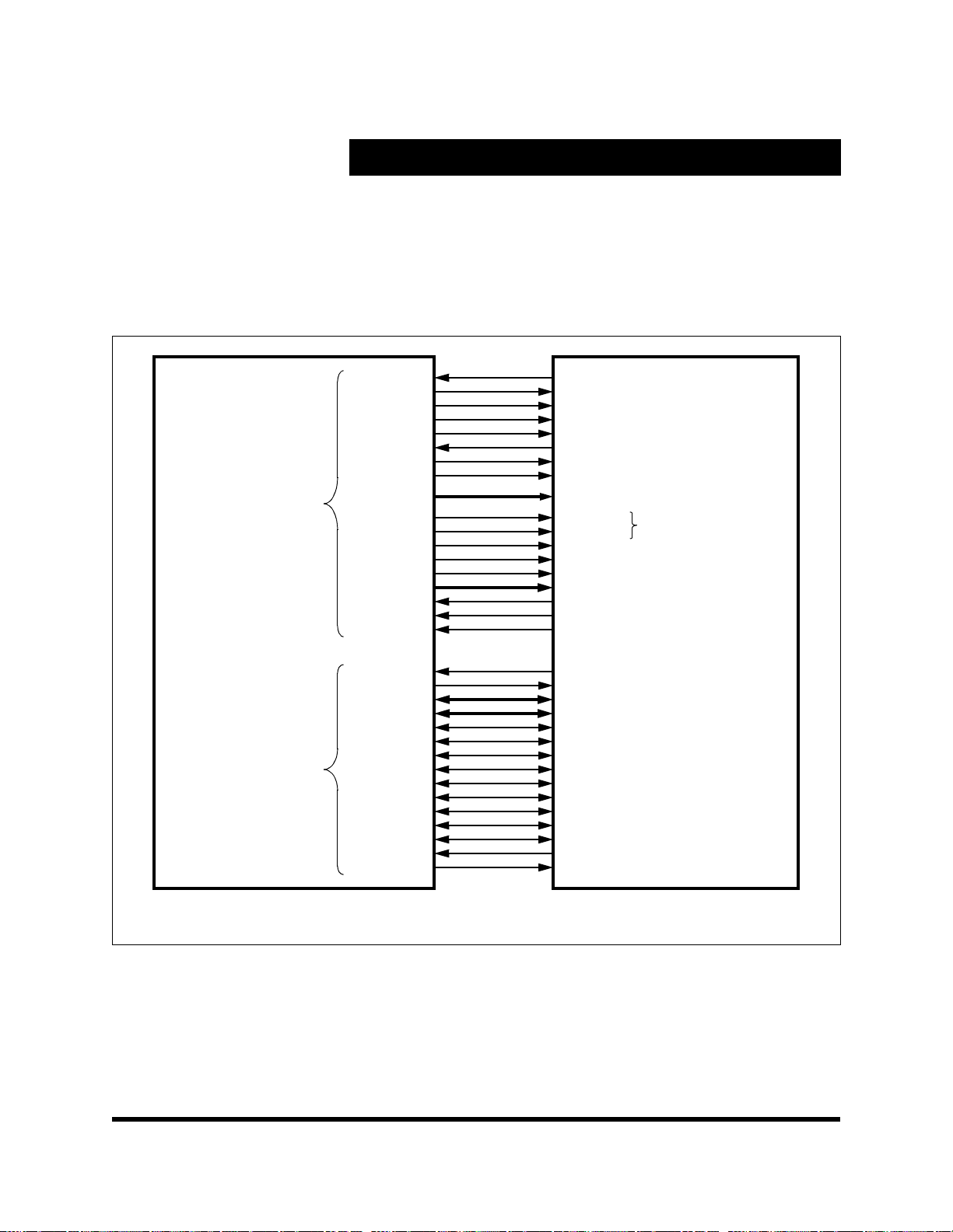
Subsystem Signal Connections
2.3 Subsystem Signal Connections
As previously stated, the MediaGX Integrated
Subsystem with MMX support con sis ts of two
chips. The MediaGX MMX-Enhanced Processor
and either the Cx5520 or Cx5530 I/O Companion
Chip. Figure 2-4 shows the signal connections
between the processor and the I/O companion
chip.
Exclusive
Interconnect
Signals
(Do not connect to
any other device)
MediaGX™
MMX™-Enhanced
Processor
Nonexclusive
Interconnect
Signals
(May also connect
to other circuitry)
SYSCLK
SERIALP
IRQ13
SMI#
PCLK
DCLK DCLK
CRT_HSYNC
CRT_VSYNC
PIXEL[17:0]
FP_HSYNC
FP_VSYNC
ENA_DISP
VID_VAL
VID_CLK
VID_DATA[7:0]
VID_RDY
RESET
INTR
SUSP#
SUSPA#
AD[31:0]
C/BE[3:0]#
PAR
FRAME#
IRDY#
TRDY#
STOP#
LOCK#
DEVSEL#
PERR#
SERR#
REQ0#
(Note)
GX_CLK
PSERIAL
IRQ13
SMI#
PCLK
HSYNC
VSYNC
PIXEL[23:0]
FP_HSYNC
FP_VSYNC
FP_ENA_DISP
VID_VAL
VID_CLK
VID_DATA[7:0]
VID_RDY
CPU_RST
INTR
SUSP#
SUSPA#
AD[31:0]
C/BE[3:0]#
PAR
FRAME#
IRDY#
TRDY#
STOP#
LOCK#
DEVSEL#
PERR#
SERR#
REQ#
GNT#GNT0#
Not needed if
CRT only (no TFT)
Cx5520/Cx5530
I/O Companion
Note: Refer to Figure 2-5 for interconnection of these lines.
Figure 2-4 Subsystem Signal Connections
Page 34 Cyrix Corporation Confidential GXm_db_v2.0
Page 51
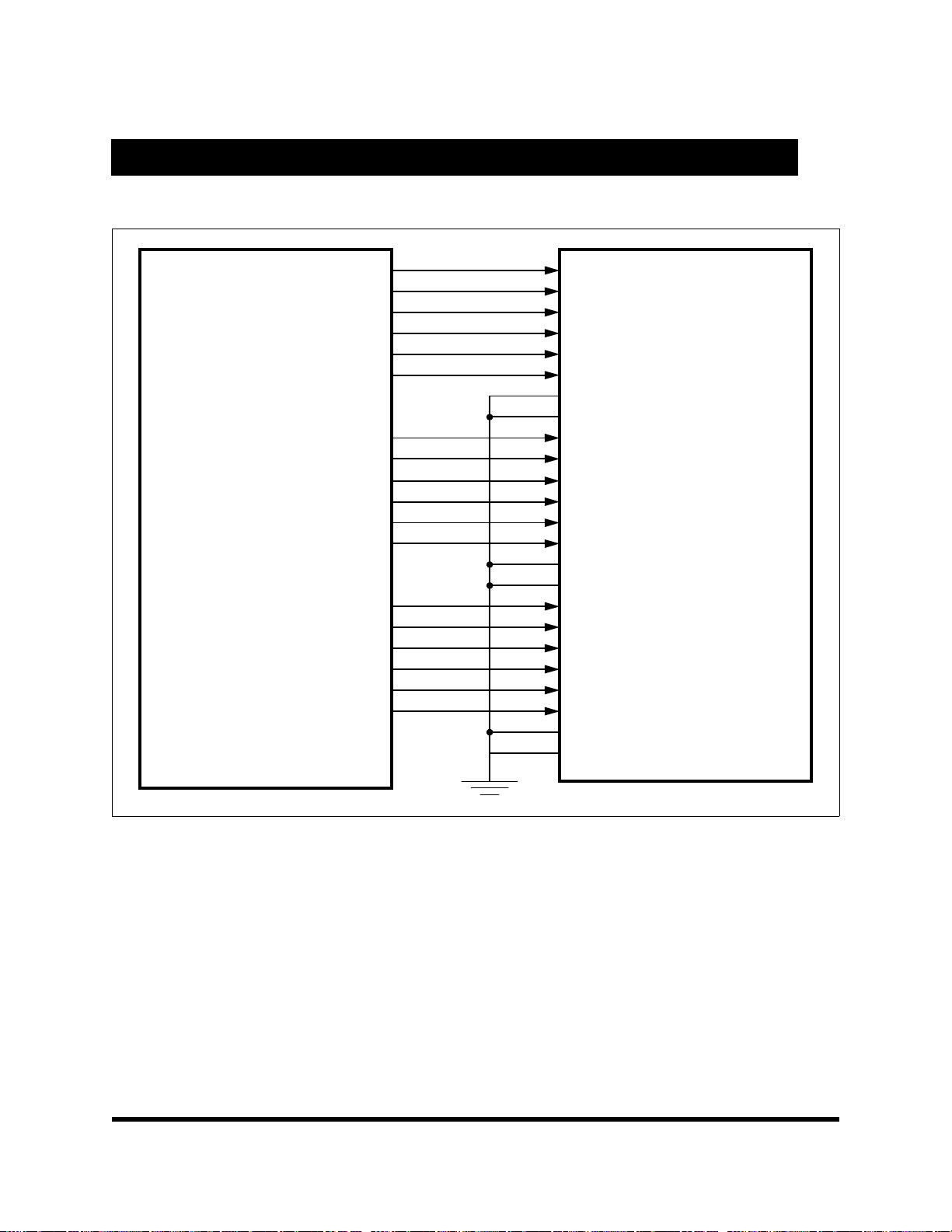
Subsystem Signal Connections
2
MediaGX™
MMX™-Enhanced
Processor
PIXEL17
PIXEL16
PIXEL15
PIXEL14
PIXEL13
PIXEL12
PIXEL11
PIXEL10
PIXEL9
PIXEL8
PIXEL7
PIXEL6
PIXEL5
PIXEL4
PIXEL3
PIXEL2
PIXEL1
PIXEL0
PIXEL23
PIXEL22
PIXEL21
PIXEL20
PIXEL19
PIXEL18
PIXEL17
PIXEL16
PIXEL15
PIXEL14
PIXEL13
PIXEL12
PIXEL11
PIXEL10
PIXEL9
PIXEL8
PIXEL7
PIXEL6
PIXEL5
PIXEL4
PIXEL3
PIXEL2
PIXEL1
PIXEL0
Cx5520/Cx5530
I/O Companion
Figure 2-5 PIXEL Signal Connections
GXm_db_v2.0 Cyrix Corporation Confidential Page 35
Page 52
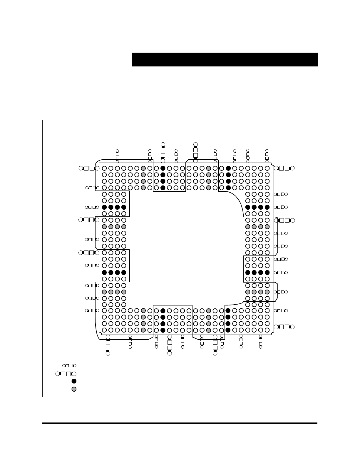
Power Planes
2.4 Power Planes
Figure 2-6 shows layout recommendations for splitting the power plane between 2.9 (V
(V
) volts in the BGA package. The illustration
CC3
) and 3.3
CC2
assumes there is one power plane, and no components on the back of the board.
3.3V Plane
(VCC3)
3.3V Plane
(VCC3)
1
A
2.9V Plane
(VCC2)
26
A
MediaGX™
MMX™-Enhanced
Processor
352 BGA - Top View
2.9V Plane
(VCC2)
AF
1
Legend
= High frequency capacitor
= 220µF, low ESR capacitor
= 3.3V connection
= 2.9V connection
Figure 2-6 BGA Recommended Split Power Plane and Decoupling
Page 36 Cyrix Corporation Confidential GXm_db_v2.0
3.3V Plane
(VCC3)
AF
26
Page 53
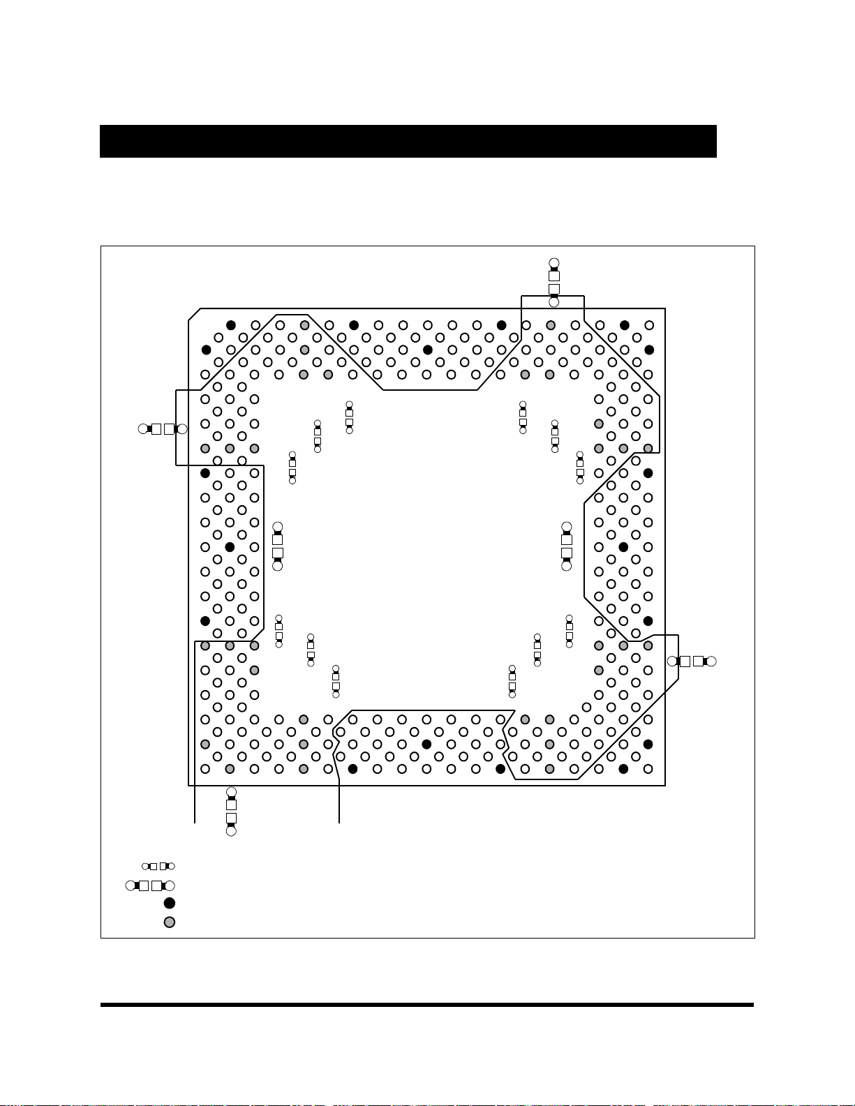
Power Planes
2
Figure 2-7 shows layout recommendations for splitting the power plane between 2.9 (V
1 37
A
) and 3.3
CC2
3.3V Plane
(VCC3)
2.9V Plane
(VCC2)
MediaGX™
MMX™-Enhanced
3.3V Plane
(VCC3)
Processor
320 SPGA - Top View
) volts in the SPGA package.
(V
CC3
A
3.3V Plane
(VCC3)
2.9V Plane
(VCC2)
Legend
AN
1 37
= High frequency capacitor
= 220µF, low ESR capacitor
= 3.3V connection
= 2.9V connection
To 2.9V
Regulator
3.3V Plane
(VCC3)
Where signals cross plane splits, it is recommended to include
Note:
AC decoupling between planes with 47pF capacitors.
AN
Figure 2-7 SPGA Recommended Split Power Plane and Decoupling
GXm_db_v2.0 Cyrix Corporation Confidential Page 37
Page 54

Power Planes
Page 38 Cyrix Corporation Confidential GXm_db_v2.0
Page 55

MediaGX™ MMX™-Enhanced Processor
Integrated x86 Solution with MMX™ Support
3 Processor Programming
This section describes the internal operations of
the MediaGX MMX-Enhanced processor from a
programmer’s point of view. It includes a description of the traditional “core” processing and FPU
operations. The integrated function registers are
described at the end of this chapter.
The primary register sets within the processor core
include:
• Application Register Set
• System Register Set
• Model Specific Register Set
• Floating Point Unit Register Set.
The initialization of the major registers within in
core are shown in Table 3-1 on page 40.
The integrated function sets are located in main
memory space and include:
• Internal Bus Int erface Unit Register Se t
• Graphics Pipeline Register Set
• Display Controller Register Set
• Memory Controller Register Set
• Power Management Register Set
3.1 Core Processor Initialization
The MediaGX processor is initialized when the
RESET signal is asserted. The processor is placed
in real mode and the registers listed in Table 3-1
are set to their initialized values. RESET invalidates and disables the CPU cache, and turns off
paging. When RESET is asserted, the CPU terminates all local bus activity and all internal execution. During the entire time that RESET is asserted,
the internal pipeline is flushed and no instruction
execution or bus activity occurs.
Approximately 150 to 250 external clock cycles
after RESET is deasserted, the processor begins
executing instructions at the top of physical
memory (address location FFFF FFF0h). The actual
time depends on the clock scaling in use. Also, an
additional 2
test is requested.
Typically, an intersegment jump is placed at FFFF
FFF0h. This instruction will force the processor to
begin execution in the lowest 1MB of address
space.
The following table, Table 3-1, lists the core registers and illustrates how they are initialized.
20
clock cycles are needed when self-
GXm_db_v2.0 Cyrix Corporation Confidential Page 39
Page 56

Core Processor Initialization
g
g
g
g
g
g
g
g
g
g
g
g
g
g
g
g
g
g
g
g
g
g
g
g
g
g
g
Table 3-1 Initialized Core Register Controls
Register Register Name Initialized Contents Comments
EAX Accumulator xxxx xxxxh 0000 0000h indicates self-test passed.
EBX Base xxxx xxxxh
ECX Count xxxx xxxxh
EDX Data xxxx 04 [DIR0] DIR0 = Device ID
EBP Base Pointer xxxx xxxxh
ESI Source Index xxxx xxxxh
EDI Destination Index xxxx xxxxh
ESP Stack Pointer xxxx xxxxh
EFLAGS Fla
EIP Instruction Pointer 0000 FFF0h
ES Extra Se
CS Code Se
SS Stack Se
DS Data Se
FS Extra Se
GS Extra Se
IDTR Interrupt Descriptor Table
GDTR Global Descriptor Table
LDTR Local Descriptor Table Re
TR Task Re
CR0 Machine Status Word 6000 0010h See Table 3-7 on pa
CR2 Control Re
CR3 Control Re
CR4 Control Re
CCR1 Confi
CCR2 Confi
CCR3 Confi
CCR7 Confi
SMAR0 SMM Address 0 00h See Table 3-11 on pa
SMAR1 SMM Address 1 00h See Table 3-11 on pa
SMAR2 SMM Address 2 / SMAR Size 00h See Table 3-11 on pa
DIR0 Device Identification 0 4xh Device ID and reads back initial CPU clock-
DIR1 Device Identification 1 xxh Steppin
DR7 Debu
Note:
x = Undefined value
s 0000 0002h See Table 3-4 on page 45 for bit definitions.
ment 0000h Base address set to 0000 0000h.
ment F000h Base address set to FFFF 0000h.
ment 0000h Base address set to 0000 0000h.
ment 0000h Base address set to 0000 0000h.
ment 0000h Base address set to 0000 0000h.
ment 0000h Base address set to 0000 0000h.
ister
Re
Re
ister
ister xxxxh
ister 2 xxxx xxxxh See Table 3-7 on page 48 for bit definitions.
ister 3 xxxx xxxxh See Table 3-7 on page 48 for bit definitions.
ister 4 0000 0000h See Table 3-7 on page 48 for bit definitions.
uration Control 1 00h See Table 3-11 on page 52 for bit definitions.
uration Control 2 00h See Table 3-11 on page 52 for bit definitions.
uration Control 3 00h See Table 3-11 on page 53 for bit definitions.
uration Control 7 00h See Table 3-11 on page 54 for bit definitions.
Register 7 0000 0400h See Table 3-13 on page 58 for bit definitions.
Base = 0, Limit = 3FFh
xxxx xxxxh xxxxh
ister xxxx xxxxh, xxxxh
Limit set to FFFFh.
Limit set to FFFFh.
Limit set to FFFFh.
Limit set to FFFFh.
Limit set to FFFFh.
Limit set to FFFFh.
speed settin
See Table 3-11 on pa
See Table 3-11 on pa
.
and Revision ID (RO).
e 48 for bit definitions.
e 55 for bit definitions.
e 55 for bit definitions.
e 55 for bit definitions.
e 56 for bit definitions.
e 56 for bit definitions.
Page 40 Cyrix Corporation Confidential GXm_db_v2.0
Page 57

Instruction Set Overview
3
3.2 Instruction Set Overview
The MediaGX processor instruction set can be
divided into nine types of operations:
• Arithmetic
• Bit Manipulation
• Shift/Rotate
• String Manipulation
• Control Transfer
• Data Transfer
• Floating Point
• High-Level Language Support
• Operating System Support
MediaGX processor instructions operate on as few
as zero operands and as many as three operands.
An NOP instruction (no operation) is an example of
a zero-operand instruction. Two-operand instructions allow the specification of an explicit source
and destination pair as part of the instruction.
These two-operand instructions can be divided into
ten groups according to operand types:
• Register to Register
• Register to Memory
• Memory to Register
• Memory to Memory
• Register to I/O
• I/O to Register
• Memory to I/O
• I/O to Memory
• Immediate Data to Register
• Immediate Data to Memory
An operand can be held in the instruction itself (as
in the case of an immediate operand), in one of the
processor’s registers or I/O ports, or in memory. An
immediate operand is fetched as part of the
opcode for the instruction.
Operand lengths of 8, 16, 32 or 48 bits are
supported as well as 64 or 80 bits associated with
floating-point instructions. Operand lengths of 8 or
32 bits are generally used when executing code
written for 386- or 486-class (32-bit code) processors. Operand lengths of 8 or 16 bits are generally
used when executing existing 8086 or 80286 code
(16-bit code). The default length of an operand can
be overridden by placing one or more instruction
prefixes in front of the opcode. For example, the
use of prefixes allows a 32-bit operand to be used
with 16-bit code or a 16-bit operand to be used with
32-bit code.
Section 9.1 “General Instruction Set Format” on
page 234 contains the clock count table that lists
each instruction in the CPU instruction set.
Included in the table are the associated opcodes,
execution clock counts, and effects on the Flags
register.
3.2.1 Lock Prefix
The LOCK prefix may be placed before certain
instructions that read, modify, then write back to
memory. The PCI will not be granted access in the
middle of locked instructions. The LOCK prefix can
be used with the following instructions only when
the result is a write operation to memory.
Bit Test Instructions (BTS, BTR, BTC)
Exchange Instructions (XADD, XCHG,
CMPXCHG)
One-Operand Arithmetic and Logical Instruc-
tions (DEC, INC, NEG, NOT)
Two-Operand Arithmetic and Logical Instruc-
tions (ADC, ADD, AND, OR, SBB, SUB,
XOR).
An invalid opcode exception is generated if the
LOCK prefix is used with any other instruction or
with one of the instructions above when no write
operation to memory occurs (for example, when
the destination is a register).
GXm_db_v2.0 Cyrix Corporation Confidential Page 41
Page 58
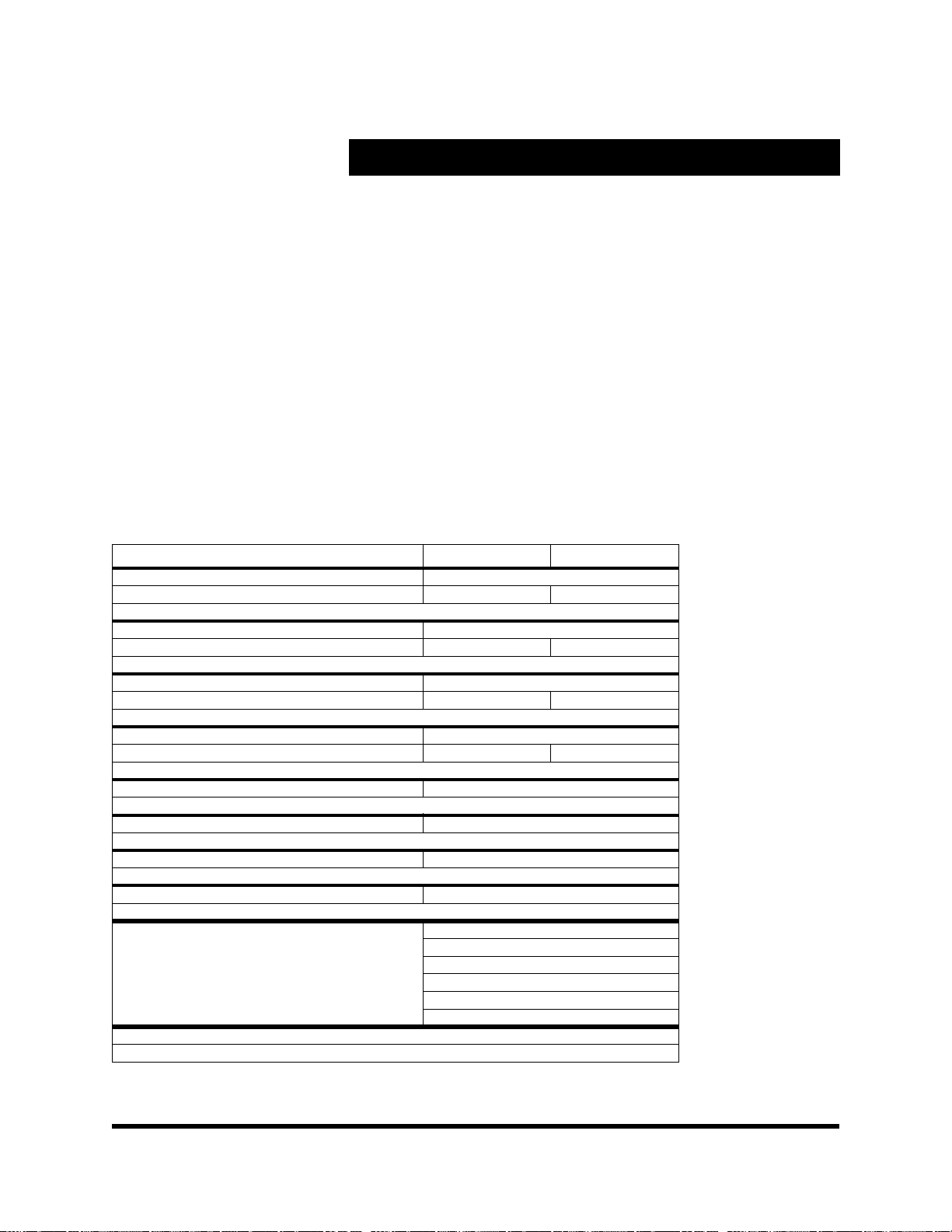
Register Sets
3.3 Register Sets
The accessible registers in the processor are
grouped into three sets:
1) The
Application Register Set
contains the
registers frequently used by application
programmers. Table 3-2 shows the general
purpose registers, segment registers, the
instruction pointer register and the flag register.
2) The
System Register Set
contains the registers typically reserved for operating-systems
programmers: control registers, system
address registers, debug registers, configuration registe rs, and test registers.
Table 3-2 Application Register Set
31 16 15 8 7 0
EAX (Extended A Register)
EBX (Extended B Register)
ECX (Extended C Register)
EDX (Extended D Register)
ESI (Extended Source Index)
EDI (Extended Destination Index)
EBP (Extended Base Pointer)
ESP (Extended Stack Pointer)
EIP (Extended Instruction Pointer Register) Instruction Pointer and
EFLAGS (Extended Flags Register) Flags Register
3) The
Model Specific Register (MSR) Set
used to monitor the performance of the
processor or a specific component within the
processor. The model specific register set has
one 64-bit register called the Time Stamp
Counter.
Each of these register sets are discussed in detail
in the subsections that follow. Additional registers
to support integrated MediaGX processor
subsystems are described in Section 4.1 “Integrated Functions Programming Interface” of this
manual.
AX
AH AL
BX
BH BL
CX
CH CL
DX
DH DL
SI (Source Index)
DI (Destination Index)
BP (Base Pointer)
SP (Stack Pointer)
CS (Code Segment)
SS (Stack Segment)
DS (D Data Segment)
ES (E Data Segment)
FS (F Data Segment)
GS (G Data Segment)
is
General
Purpose
Registers
Segment
(Selector)
Registers
Page 42 Cyrix Corporation Confidential GXm_db_v2.0
Page 59

Register Sets
3
3.3.1 Application Register Set
The Application Register Set consists of the registers most often used by the applications
programmer. These registers are generally accessible, although some bits in the Flags register are
protected.
The
General Purpose Register
frequently modified by instructions and typically
contain arithmetic and logical instruction operands.
In real mode,
base address for each segment. In protected
mode, the segment registers contain segment
selectors. The segment selectors provide indexing
for tables (located in memory) that contain the
base address for each segment, as well as other
memory addressing information.
The
Instruction Pointer Register
next instruction that the processor will execute.
This register is automatically incremented by the
processor as execution progresses.
The
Flags Register
reflect the status of previously executed instructions. This register also contains control bits that
affect the operation of some instructions.
Segment Registers
contains control bits used to
contents are
contain the
points to the
3.3.1.1 General Purpose Registers
The General Purpose Registers are divided into
four data register s, two pointe r registe rs, an d two
index registers as shown in Table 3-2 on page 42.
The
Data Registers
programmer to manipulate data structures and to
hold the results of logical and arithmetic operations. Different portions of general data registers
can be addressed by using different names.
An “E” prefix identifies the complete 32-bit register.
An “X” suffix without the “E” prefix identifies the
lower 16 bits of the register.
are used by the applications
The lower two bytes of a data register are
addressed with an “H” suffix (identifies the upper
byte) or an “L” suffix (identifies the lower byte).
These _L and _H portions of the data registers act
as independent registers. For example, if the AH
register is written to by an instruction, the AL
register bits remain unchanged.
The
Pointer and Index Registers
SI or ESI Source Index
DI or EDI Destination Index
SP or ESP Stack Pointer
BP or EBP Base Pointer
These registers can be addressed as 16- or 32-bit
registers, with the “E” prefix indicating 32 bits. The
pointer and index registers can be used as general
purpose registers; however, some instructions use
a fixed assignment of these registers. For example,
repeated string operations always use ESI as the
source pointer, EDI as the destination pointer, and
ECX as a counter. The instructions that use fixed
registers include multiply and divide, I/O access,
string operations, stack operations, loop, variable
shift and rotate, and translate instructions.
The MediaGX processor implements a stack using
the ESP register. This stack is accessed during th e
PUSH and POP instructions, procedure calls,
procedure returns, interrupts, exceptions, and
interrupt/exception returns. The MediaGX
processor automatically adjusts the value of the
ESP during operations that result from these
instructions.
The EBP register may be used to refer to data
passed on the stack during procedure calls. Local
data may also be placed on the stack and
accessed with BP. This register provides a mechanism to access tack data in high-level languages.
are listed below.
GXm_db_v2.0 Cyrix Corporation Confidential Page 43
Page 60
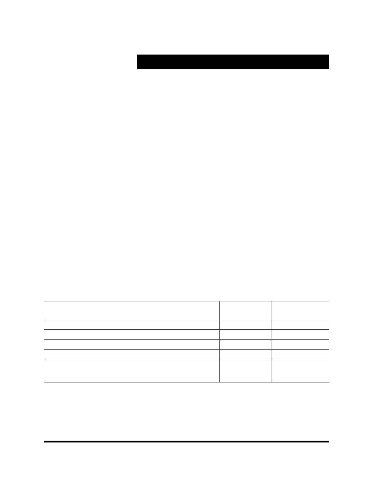
Register Sets
3.3.1.2 Segment Registers
The 16-bit segment registers, part of the main
memory addressing mechanism, are described in
Section 3.5 “Offset, Segm ent, an d Paging Mech anisms” on page 66. The six segment registers are:
CS - Code Segment
DS - Data Segment
SS - Stack Segment
ES - Extra Segment
FS - Additional Data Segment
GS - Additional Data Segment
The segment registers are used to select
segments in main memory. A segment acts as
private memory for different elements of a program
such as code space, data space and stack space.
There are two segment mechanisms, one for Real
and Virtual 8086 Operating Modes and one for
Protective Mode. Initialization and transition to
protective mode is described in Section 3.13.4
“Initialization and Transition to Protected Mode” on
page 99. The segment mechanisms are described
in Section 3.7 “Descriptors and Segment Mechanisms” on page 68.
The active segment register is selected according
to the rules listed in Table 3-3 and the type of
instruction being currently processed. In general,
the DS register selector is used for data references. Stack references use the SS register, and
instruction fetches use the CS register. While some
of these selections may be overridden, instruction
fetches, stack operations, and the destination write
operation of string operations cannot be overridden. Special segment-override instruction
prefixes allow the use of alternate segment registers. These segment registers include the ES, FS,
and GS registers.
3.3.1.3 Instruction Pointer Register
The
Instruction Pointer (EIP) Register
the offset into the current code segment of the next
instruction to be executed. The register is normally
incremented by the length of the current instruction
with each instruction execution unless it is implicitly
modified through an interrupt, exception, or an
instruction that chang es the se quen tia l exe cu tio n
flow (for example JMP and CALL).
Table 3-3 illustrates the code segment selection
rules.
contains
Table 3-3 Segment Register Selection Rules
Implied (Default)
Type of Memory Reference
Code Fetch CS None
Destination of PUSH, PUSHF, INT, CALL, PUSHA instructions SS None
Source of POP, POPA, POPF, IRET, RET instructions SS None
Destination of STOS, MOVS, REP STOS, REP MOVS instructions ES None
Other data references with effective address using base registers of:
EAX, EBX, ECX, EDX, ESI, EDI, EBP, ESP
Page 44 Cyrix Corporation Confidential GXm_db_v2.0
Segment
DS
SS
Segment-Override
Prefix
CS, ES, FS, GS, SS
CS, DS, ES, FS, GS
Page 61

3.3.1.4 Flags Register
The Flags Register contains status information and
controls certain operations on the MediaGX
processor. The lower 16 bits of this register are
Table 3-4 EFLAGS Register
Bit Name Flag Type Description
31:22 RSVD --
21 ID System
20:19 RSVD --
18 AC System
17 VM System
16 RF Debug
15 RSV D -14 NT System
13:12 IOPL System
11 OF Arithmetic
10 DF Control
9IFSystem
8 TF Debug
7 SF Arithmetic
6 ZF Arithmetic
5 RSVD -4 AF Arithmetic
3 RSVD -2 PF Arithmetic
1 RSVD
0 CF Arithmetic
Reserved
Identification Bit
supported. The ID can be modified only if the CPUID bit in CCR4 (Index E8h[7]) is set.
Reserved
Alignment Check Enable
whether or not misaligned accesses to memory cause a fault. If AC is set, alignment faults are
enabled.
Virtual 8086 Mode
operation handling segment loads as the 8086 does, but generating exception 13 faults on
privileged opcodes. The VM bit can be set by the IRET instruction (if current privilege level
is 0) or by task switches at any privilege level.
Resume Flag
instruction boundaries before breakpoint exception processing. If set, any debug fault is
ignored on the next instruction.
Reserved
Nested Task
current task is nested within another task.
I/O Privilege Level
rent privilege level (CPL) permitted to execute I/O instructions without generating an exception
13 fault or consulting the I/O permission bit map. IOPL also indicates the maximum CPL allowing alteration of the IF bit when new values are popped into the EFLAGS register.
Overflow Flag
but did not result in a carry or borrow out of the high-order bit. Also set if the operation resulted
in a carry or borrow out of the high-order bit but did not result in a carry or borrow into the sign
bit of the result.
Direction Flag
appropriate index registers (ESI and/or EDI). Setting DF causes auto-decrement of the index
registers to occur.
Interrupt Enable Flag
and serviced by the CPU.
Trap Enable Flag
pletes execution. TF is cleared by the single-step interrupt.
Sign Flag
Zero Flag
Reserved
Auxiliary Carry Flag
tion 3 of the result occurs; cleared otherwise.
Reserved
Parity Flag
otherwise PF is cleared.
Reserved
Carry Flag
cant bit of the result occurs; cleared otherwise.
— Set to 0.
— The ability to set and clear this bit indicates that the CPUID instruction is
— Set to 0.
— If set while in protected mode, the processor switches to virtual 8086
— Used in conjunction with debug register breakpoints. RF is checked at
— Set to 0.
— While executing in protected mode, NT indicates that the execution of the
— While executing in protected mode, IOPL indicates the maximum cur-
— Set if the operation resulted in a carry or borrow into the sign bit of the result
— When cleared, DF causes string instructions to auto-increment (default) the
— When set, maskable interrupts (INTR input pin) are acknowledged
— Once set, a single-step interrupt occurs after the next instruction com-
— Set equal to high-order bit of result (0 indicates positive, 1 indicates negative).
— Set if result is zero; cleared otherwise.
— Set to 0.
— Set when a carry out of (addition) or borrow into (subtraction) bit posi-
— Set to 0.
— Set when the low-order 8 bits of the result contain an even number of ones;
— Set to 1.
— Set when a carry out of (addition) or borrow into (subtraction) the most signifi-
Register Sets
3
referred to as the Flags register that is used when
executing 8086 or 80286 code. Table 3-4 gives the
bit formats for the EFLAGS Register.
— In conjunction with the AM flag in CR0, the AC flag determines
GXm_db_v2.0 Cyrix Corporation Confidential Page 45
Page 62
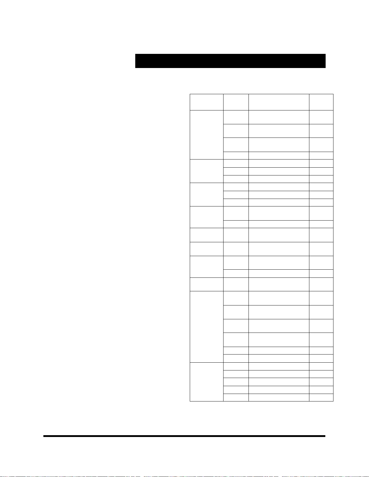
Register Sets
3.3.2 System Register Set
The system register set, shown in Table 3-5,
consists of registers not generally used by application programmers. These registers are typically
employed by system level programmers who
generate operating systems and memory management programs. Associated with the system
register set are certain tables and segments which
are listed in Table 3-5.
The Control Registers control certain aspects of
the MediaGX processor such as paging, coprocessor functions, and segment protection.
The Descriptor Tables hold descriptors that
manage memory segments and tables, interrupts
and task switching. The tables are defined by
corresponding registers.
The two Task State Segments Tables defined by
TSS register are used to save and load the
computer state when switching tasks.
The Configuration Registers are used to define
Cyrix MediaGX CPU setup including cache
management.
The ID registers allow BIOS and other software to
identify the specific CPU and stepping. Sys tem
Management Mode (SMM) control information is
stored in the SMM registers.
The Debug Registers provide debugging facilities
for the MediaGX processor and enable the use of
data access breakpoints and code execution
breakpoints.
The Test Registers provide a mechanism to test
the contents of both the on-chip 16KB cache and
the Translation Lookaside Buffer (TLB). The TLB is
used as a cache for the tables that are used in to
translate linear addresses to physical addresses
while paging is enabled.
Table 3-5 lists the system register sets along with
their size and function.
Table 3-5 System Register Set
Group Name Function
Control
Registers
Descriptor
Tables
Descriptor
Table
Registers
Task State
Segment and
Registers
Configuration
Registers
ID
Registers
SMM
Registers
Performance
Registers
Debug
Registers
Test
Registers
CR0 System Control
Register
CR2 Page Fault Linear
Address Register
CR3 Page Directory Base Reg-
ister
CR4 Time Stamp Counter 32
GDT General Descriptor Table 32
IDT Interrupt Descriptor Table 32
LDT Local Descriptor Table 16
GDTR GDT Register 32
IDTR IDT Register 32
LDTR LDT Register 16
TSS Task State Segment
Tables
TR TSS Register Setup 16
CCRn Configuration Control
Registers
DIRn Device Identification
Registers
SMARn SMM Address Region
Registers
SMHRn SMM Header Addresses 8
PCR0 Performance Control
Register
DR0 Linear Breakpoint
Address 0
DR1 Linear Breakpoint
Address 1
DR2 Linear Breakpoint
Address 2
DR3 Linear Breakpoint
Address 3
DR6 Breakpoint Status 32
DR7 Breakpoint Control 32
TR3 Cache Test 32
TR4 Cache Test 32
TR5 Cache Test 32
TR6 TLB Test Control 32
TR7 TLB Test Status 32
Width
(Bits)
32
32
32
16
8
8
8
8
32
32
32
32
Page 46 Cyrix Corporation Confidential GXm_db_v2.0
Page 63
Register Sets
3
3.3.2.1 Control Registers
A map of the Control Registers (CR0, CR2, CR3,
and CR4) is shown in Table 3-6 and the bit de fi nitions given in Table 3-7. ( These r egi sters sh ould not
be confused with the CRRn registers.) The CR0
register contains system control bits which
state of t he CPU. The lower 16 bits of CR0 are
referred to as the Machine Status Word (MSW).
When operating in real mode, any program can read
and write the control registers. In protected mode,
however, only privilege level 0 (most-privileged)
programs can read and write these registers.
configure operating modes and indicate the ge neral
Table 3-6 Control Registers Map
313029282726252423222120191817161514131211109876543210
CR4 Register
RSVD T
CR3 Register
PDBR (Page Directory Base Register) RSVD 0 0 RSVD
CR2 Register
PFLA (Page Fault Linear Address)
CR1 Register
RSVD
RSVD
S
C
CR0 Register
PGCDN
W
RSVD AMR
W
S
P
V
D
RSVD NE1TSEMMPP
E
Machine Status Word (MSW)
GXm_db_v2.0 Cyrix Corporation Confidential Page 47
Page 64
Register Sets
g
ging
g
ging
g
g
g
g
g
g
g
g
g
g
g
g
g
g
Table 3-7 CR4-CR0 Bit Definitions
Bit Name Description
CR4 Register
31:3 RSVD
2TSC
1:0 RSVD
CR3 Register
31:12 PDBR
11:0 RSVD
CR2 Register
31:0 PFLA
CR0 Register
31 PG
30 CD
29 NW
18 AM
16 WP
5NE
41
3TS
2EM
1MP
0PE
Reserved:
Time Stamp Counter Instruction:
If = 1 RDTSC instruction enabled for CPL = 0 only; reset state.
If = 0 RDTSC instruction enabled for all CPL states.
Reserved
Page Directory Base Register:
Reserved:
Page Fault Linear Address:
the address that caused the pa
Paging Enable Bit:
state of PG, software must execute an unconditional branch instruction (e.
take effect.
Cache Disable:
to be used if the requested address hits in the cache. Writes continue to update the cache and cache invalidations due to inquiry cycles occur normally . The cache must also be invalidated to completely disable any cache
activity.
Not Write-Through:
issued to the external bus only for a cache miss, a line replacement of a modified line, execution of a locked
instruction, or a line eviction as the result of a flush cycle. If NW = 0, the on-chip cache operates in write-throu
mode. In write-throu
chan
Alignment Check Mask:
ment check faults. Settin
Write Protect:
written from privile
Numerics Exception:
are to be handled by external interrupts.
Reserved:
Task Switched:
TS = 1 causes a DNA fault. If MP = 1 and TS = 1, a WAIT instruction also causes a DNA fault.
Emulate Processor Extension:
Monitor Processor Extension:
fault 7. The TS bit is set to 1 on task switches by the CPU. Floatin
state of the MP bit. The MP bit should be set to one durin
Protected Mode Enable:
enabled. If PE = 0, the CPU operates in real mode and addresses are formed as in an 8086-style CPU. Refer to
Section 3.13 “Protection” on pa
Set to 0 (always returns 0 when read).
— Set to 0 (always returns 0 when read).
Set to 0.
If PG = 1 and protected mode is enabled (PE = 1), pa
If CD = 1, no further cache line fills occur. However , data already present in the cache continues
If NW = 1, the on-chip cache operates in write-back mode. In write-back mode, writes are
h mode, all writes (including cache hits) are issued to the external bus. This bit cannot be
ed if LOCK_NW = 1 in CCR2.
If AM = 1, the AC bit in the EFLAGS re
AM = 0 prevents AC faults from occurring.
Protects read-only pa
e level 0-2. WP = 1 forces a fault on a write to a read-only page from any privilege level.
NE = 1 to allow FPU exceptions to be handled by interrupt 16. NE = 0 if FPU exceptions
Do not attempt to modify.
Set whenever a task switch operation is performed. Execution of a floatin
Enables the se
Identifies pa
With pa
e fault.
If EM = 1, all floatin
If MP = 1 and TS = 1, a WAIT instruction causes Device Not Available (DNA)
e 97.
e directory base address on a 4KB page boundary.
enabled and after a page fault, PFLA contains the linear address of
is enabled. After changing the
., JMP, CALL) to have the change
ister is unmasked and allowed to enable align-
es from supervisor write access. WP = 0 allows a read-only page to be
point instruction with
point instructions cause a DNA fault 7.
point instructions are not affected by the
normal operations.
ment based protection mechanism. If PE = 1, protected mode is
h
Page 48 Cyrix Corporation Confidential GXm_db_v2.0
Page 65
Table 3-8 Effects of Various Combinations of EM, TS, and MP Bits
CR0[3:1] Instruction Type
TS EM MP WAIT ESC
0 0 0 Execute Execute
0 0 1 Execute Execute
1 0 0 Execute Fault 7
1 0 1 Fault 7 Fault 7
0 1 0 Execute Fault 7
0 1 1 Execute Fault 7
1 1 0 Execute Fault 7
1 1 1 Fault 7 Fault 7
Register Sets
3
GXm_db_v2.0 Cyrix Corporation Confidential Page 49
Page 66

Register Sets
3.3.2.2 Configuration Registers
The configuration registers listed in Table 3-9 are
CPU registers and are selected by register index
numbers. The registers are accessed through I/O
memory locations 22h and 23h. Registers are
selected for access by writing an index number to
I/O Port 22h using an OUT instruction prior to
transferring data through I/O Port 23h.
Each data transfer through I/O Port 23h must be
preceded by a register index selection through I/O
Port 22h; otherwise, subsequent I/O Port 23h operations are directed off-chip and produce external
I/O cycles.
If MAPEN, bit 4 of CCR3 (Index C3h[4]) = 0,
external I/O cycles will occur if the register index
number is outside the range C0h-CFh, FEh, and
FFh. The MAPEN bit should remain 0 during
normal operation to allow system registers located
at I/O Port 22h to be accessed (see Table 3-11 on
page 53).
Table 3-9 Configuration Register Summary
Access
Index Type Name
C1h R/W CCR1 — Configuration Control 1 SMI_LOCK 00h Table 3-11 on page52
C2h R/W CCR2 — Configuration Control 2 -- 00h Table 3-11 on page 52
C3h R/W CCR3 — Configuration Control 3 SMI_LOCK 00h Table 3-11 on page 53
E8h R/W CCR4 — Configuration Control 4 MAPEN 85h Table 3-11 on page 54
EBh R/W CCR7 — Configuration Control 7 -- 00h Table 3-11 on page 54
20h R/W PCR — Performance Control MAPEN 07h Table 3-11 on page 54
B0h R/W S MHR0 — SMM Header Address 0 MAPEN xxh Table 3-11 on page 55
B1h R/W S MHR1 — SMM Header Address 1 MAPEN xxh Table 3-11 on page 55
B2h R/W S MHR2 — SMM Header Address 2 MAPEN xxh Table 3-11 on page 55
B3h R/W S MHR3 — SMM Header Address 3 MAPEN xxh Table 3-11 on page 55
B8h R/W GCR — Graphics Control Register MAPEN 00h Table 4-1 on page 104
B9h VGACTL — VGA Control Register -- 00h Table 5-5 on page 200
BAh-BDh VGAM0 — VGA Mask Register -- 00h Table 5-5 on page 200
CDh R/W SMAR0 — SMM Address 0 SMI_LOCK 00h Table 3-11 on page 55
CEh R/W SMAR1 — SMM Address 1 SMI_LOCK 00h Tabl e 3-11 on page 55
CFh R/W SMAR2 — SMM Address 2 SMI_LOCK 00h Table 3-11 on page 55
FEh RO DIR0 — Device ID 0 -- 4xh Table 3-11 on page 56
FFh RO DIR1 — Device ID 1 -- xx h Table 3-11 on page 56
MAPEN = Index C3h[4] (CCR3) and SMI_LOCK = Index C3h[0] (CCR3).
*Note:
Controlled By*
Default
Value
Reference
(Bit Formats)
Page 50 Cyrix Corporation Confidential GXm_db_v2.0
Page 67
Register Sets
g
g
g
g
Table 3-10 Configuration Register Map
Register
(Index) Bit 7 Bit 6 Bit 5 Bit 4 Bit 3 Bit 2 Bit 1 Bit 0
Control Registers
CCR1 (C1h)
CCR2 (C2h) USE_SUS P
CCR3 (C3h) LSS_34 LSS_23 LSS_12 MAPEN
CCR4 (E8h) CPUID SMI_NEST
CCR7 (EBh)
PCR (20h) LSSER
Device ID Registers
DIR0 (FEh) DID3 DID2 DID1 D ID0
DIR1 (FFh) SID3 SID2 SID 1 SID0 RID3 RID2 RID1 RID0
SMM Base Header Address Registers
SMAR0 (CDh) A31 A30 A29 A28 A27 A26 A25 A24
SMAR1 (CEh) A23 A22 A21 A20 A19 A18 A17 A16
SMAR2 (CFh) A15 A14 A13 A12 SIZE3 SIZE2 SIZE1 SIZE0
SMHR0 (B0h) A7 A6 A5 A4 A3 A2 A1 A0
SMHR1 (B1h) A15 A14 A13 A12 A11 A10 A9 A8
SMHR2 (B2h) A23 A22 A21 A20 A19 A18 A17 A16
SMHR3 (B3h) A31 A30 A29 A28 A27 A26 A26 A24
Graphics/VGA Related Registers
GCR (B8h)
VGACTL
(B9h)
VGAM0 (BAh) VGA Mask R e
VGAM1 (BBh) V GA Mask Re
VGAM2 (BCh) VGA Mask Re
VGAM3 (BDh) VGA Mask Re
RSVD SMAC USE_SMI RSVD
RSVD WT1 SUSP_HLT LOCK_NW RSVD
RSVD NMI_EN SMI_LOCK
RSVD DTE_EN MEM_BYP IORT2 IORT1 IORT0
RSVD NMI RSVD EMMX
RSVD
RSVD CLKMODE1 RSVD CLMODE0
RSVD Scratchpad Size Base Address Code
RSVD Enable SMI
for VGA
memory
B8000h to
BFFFFh
ister Bits [7:0 ]
ister Bits [15:8]
ister Bits [23:16]
ister Bits [31:24]
Enable SMI
for VGA
memory
B0000h to
B7FFFh
Enable SMI
for VGA
memory
A0000h to
AFFFFh
3
GXm_db_v2.0 Cyrix Corporation Confidential Page 51
Page 68
Register Sets
g
g
g
g
g
g
ging
g
Table 3-11 Configuration Registers
Bit Name Description
Index C1h CCR1 — Configuration Control Register 1 (R/W) Default Value = 00h
7:3 RSVD
2 SMAC
1USE_SMI
0RSVD
Note:
Bits 1 and 2 are cleared to zero at reset.
Index C2h CCR2 — Configuration Control Register 2 (R/W) Default Value = 00h
7 USE_SUSP
6:5 RSVD
4 WT1
3 SUSP_HLT
2LOCK_NW
1:0 RSVD
Note:
All bits are cleared to zero at reset.
Reserved:
System Management Memory Access:
If = 1: SMINT instruction can be reco
If = 0: SMINT instruction has no affect.
Note:
Enable SMM Pins:
If = 1: SMI# input pin is enabled (see Table 3-33 on pa
If = 0: SMI# pin is i
Note:
Reserved
Enable Suspend Pins:
If = 1: SUSP# input and SUSPA# output are enabled.
If = 0: SUSP# input is i
Reserved:
Write-Through Region 1
If = 1: Forces all writes to the address re
issued on the external bus.
Suspend on HALT:
If = 1: CPU enters suspend mode followin
Lock NW Bit:
If = 1: Prohibits chan
Set to 1 after settin
Reserved:
Set to 0.
nized (see Table 3-33 on page 88).
SMI_LOCK (CCR3[0]) must = 0, or the CPU must be in SMI mode, to write this bit.
e 88). SMINT instruction can be recognized.
nored.
SMI_LOCK (CCR3[0]) must = 0, or the CPU must be in SMI mode, to write this bit.
— Set to 0.
nored and SUSPA# output floats.
Set to 0.
:
ion between 640KB to 1MB that hit in the on-chip cache to be
execution of a HALT instruction.
the state of the NW bit (CR0[29]) (refer to Table 3-7 on page 48).
NW.
Set to 0.
Page 52 Cyrix Corporation Confidential GXm_db_v2.0
Page 69

Register Sets
g
g
g
g
g
g
g
g
g
g
Table 3-11 Configuration Registers (cont.)
Bit Name Description
Index C3h CCR3 — Configuration Control Register 3 (R/W) Default Value = 00h
7 LSS_34
6 LSS_23
5 LSS_12
4 MAPEN
3:2 RSVD
1NMI_EN
0 SMI_LOCK
Note:
All bits are cleared to zero at reset.
Load/Store Serialize 3 GBytes to 4 GBytes:
If = 1: Stron
Load/Store Serialize 2 GBytes to 3 GBytes:
If = 1: Stron
Load/Store Serialize 1 GByte to 2 GBytes
If = 1: Stron
Map Enable:
If = 1: All confi
If = 0: Only confi
sible. Other confi
sible.
Reserved:
NMI Enable:
If = 1: NMI is enabled durin
If = 0: NMI is not reco
Note:
SMM Register Lock:
If = 1: SMM Address Re
cannot be modified unless in SMM routine. Once set, SMI_LOCK can only be cleared by assertin
RESET pin.
R/W ordering imposed in address range C000 0000h to FFFF FFFFh:
R/W ordering imposed in address range 8000 0000h to BFFF FFFFh:
:
R/W ordering imposed in address range 4000 0000h to 7FFF FFFFh
uration registers are accessible. All accesses to Port 22h are trapped.
uration registers Index C1h through CFh, FEh, FFh (CCRn, SMAR, DIRn) are acces-
uration registers (including PCR, SMHRn, GCR, VGACTL, VGAM0) are not acces-
Set to 0.
SMM.
nized during SMM.
SMI_LOCK (CCR3[0]) must = 0 or the CPU must be in SMI mode to write to this bit.
ion Register (SMAR[31:0]), SMAC (CCR1[2]), USE_SMI (CCR1[1])
3
the
GXm_db_v2.0 Cyrix Corporation Confidential Page 53
Page 70
Register Sets
g
g
g
g
g
g
g
g
g
g
g
g
g
g
Table 3-11 Configuration Registers (cont.)
Bit Name Description
Index E8h CCR4 — Configuration Control Register 4 (R/W) Default Value = 85h
7CPUID
6 SMI_NEST
5RSVD
4DTE_EN
3MEM_BYP
2:0 IORT(2:0)
Note:
MAPEN (CCR3[4]) must = 1 to read or write to this re
Enable CPUID Instruction:
If = 1: The ID bit in the EFLAGS re
as documented in Table 9-2 "Instr uction Fields" on pa
If = 0: The ID bit can not be modified and execution of the CPUID instruction causes an i nvalid opcode
exception.
SMI Nest:
If = 1: SMI interrupts can occur durin
allow hi
Reserved —
Directory Table Entry Cache:
If = 1: Enables directory table entry to be cached.
Cleared to 0 at reset.
Memory Read Bypassing:
If = 1: Enables memory read bypassin
Cleared to 0 at reset.
I/O Recovery Time
000 = No clock delay 100 = 16-clock delay
001 = 2-clock delay 101 = 32-clock delay (default value after reset)
010 = 4-clock delay 110 = 64-clock delay
011 = 8-clock delay 111 = 128-clock delay
Cleared to 0 at reset.
her-priority SMI interrupts while handling the current event
Set to 0.
: Specifies the minimum number of bus clocks between I/O accesses:
ister to be modified and execution of the CPUID instruction occurs
e 234.
SMM mode. SMI handlers can optionally set SMI_NEST high to
.
ister.
Index EBh CCR7 — Configuration Control Register 7 (R/W) Default Value = 00h
7:3 RSVD
2NMI
1RSVD
0EMMX
Index 20h PCR — Performance Control Register (R/W) Default Value = 07h
7 LSSER
6:0 RSVD
Note:
MAPEN (CCR3[4]) must = 1 to read or write to this re
Reserved:
NMI Enable:
If = 1: Non-maskable Interrupts (NMIs) are acknowled
Reserved:
Cyrix Extended MMX Instructions Enable:
If = 1: Cyrix extended MMX instructions are enabled
Load/Store Serialize Enable (Reorder Disable):
mapped I/O devices operatin
memory accesses above 1 GByte, refer to CCR3[7:5] (LSS_34, LSS_23, LSS_12.)
If =1: All memory read and write operations will occur in execution order (load/store serializin
enabled, reorderin
If =0: Memory reads and write can be reordered for optimum performance (load/store serializin
disabled, reorderin
Memory accesses in the address ran
Reserved —
Set to 0.
ed.
Set to 0.
LSSER should be set to ensure that memory-
outside of the address range 640K to 1M will operate correctly. For
disabled).
enabled).
e 640K to 1M will always be issued in execution order.
Set to 0.
ister.
Page 54 Cyrix Corporation Confidential GXm_db_v2.0
Page 71
Register Sets
g
g
g
g
g
g
g
g
g
g
Table 3-11 Configuration Registers (cont.)
Bit Name Description
Index B0h, B1h, B2h, B3h SMHR — SMI Header Address Register (R/W) Default Value = xxh
Index SMHR Bits
B3h
B2h
B1h
B0h
Note:
Index CDh, CEh, CFh SMAR — SMM Address Region/Size Register (R/W) Default Value = 00h
Index SMAR Bits
CDh
CEh
CFh[7:4]
CFh[3:0] SIZE[3:0]
Note:
[31:24]
[23:16]
[15:12]
[7:0]
MAPEN (CCR3[4]) must = 1 to read or write to this re
[31:24]
[23:16]
[15:12]
SMI_LOCK (CCR3[0]) must = 0, or the CPU must be in SMI mode, to write these re
SMM Header Address Bits [31:0]:
the SMM header space: For example, bits [31:24] correspond with Index B3h
Refer to Section 3.11.4 “SMM Confi
SMM Address Region Bits, (SMAR [A31:A12])
address for the SMM re
Bits [31:24] correspond with Index CDh
Bits [23:16] correspond with Index CEh
Bits [15:12] correspond with Index CFh[7:4]
Index CFh allows simultaneous access to SMAR address re
SIZE[3:0]. Durin
Refer to Section 3.11.4 “SMM Confi
SMM Region Size Bits, (SIZE [3: 0] )
access the lower 4-bits of port 23 hold SIZE[3:0]. Index CFh allows simultaneous access to
Durin
SMAR address re
0000 = SMM Disabled 0100 = 32KB 1000 = 512KB 1100 = 8MB
0001 = 4KB 0101 = 64KB 1001 = 1MB 1101 = 16MB
0010 = 8KB 0110 = 128KB 1010 = 2MB 1110 = 32MB
0011 = 16KB 0111 = 256KB 1011 = 4MB 1111 = 4KB (same as 0001)
ion.
access, the upper 4-bits of Port 23h hold SMAR[15:12].
ions bits SMAR[15:12] (see above) and size code bits SIZE[3:0].
SMHR address bits [31:0] contain the physical base address for
uration Registers” on page 89 for more information.
ister.
— SMAR address bits [31:12] contain the base
ions bits SMAR[15:12] and size code bits
uration Registers” on page 89 for more information.
— SIZE address bits contain the size code for the SMM re
isters/bits.
ion.
3
GXm_db_v2.0 Cyrix Corporation Confidential Page 55
Page 72

Register Sets
g
g
g
Table 3-11 Configuration Registers (cont.)
Bit Name Description
Index FEh DIR0 — Device Identification Register 0 Default Value = 4xh
7:4 DID[3:0]
3:0 MULT[3:0]
Device ID (Read Only)
Core Multiplier (Read Only)
nal descriptions pa
If DIR1 (Index FFh) is 30h-4Fh then MULT[3:0]:
0000 = SYSCLK multiplied by 4 (Test mode only)
0001 = SYSCLK multiplied by 6
0010 = SYSCLK multiplied by 4 (Test mode only)
0011 = SYSCLK multiplied by 6
0100 = SYSCLK multiplied by 7
0101 = SYSCLK multiplied by 8
0110 = SYSCLK multiplied by 7
0111 = SYSCLK multiplied by 5
1xxx = Reserved
If DIR1 (Index FFh) is 50h or greater then MULT[3 : 0 ] :
0000 = SYSCLK multiplied by 4 (Test mode only)
0001 = SYSCLK multiplied by 10
0010 = SYSCLK multiplied by 4 (Test mode only)
0011 = SYSCLK multiplied by 6
0100 = SYSCLK multiplied by 9
0101 = SYSCLK multiplied by 5
0110 = SYSCLK multiplied by 7
0111 = SYSCLK multiplied by 8
1xxx = Reserved
— Identifies device as MediaGX MMX-Enhanced processor.
— Identifies the core multiplier set by the CLKMODE[2:0] pins (see si
e 21)
-
Index FFh DIR1 -- Device Identification Register 1 Default Value = xxh
7:0 DIR1
Device Identification Revision (Read Only)
If DIR1 is 30h-33h = MediaGX MMX-Enhanced processor revision 1.0-2.3
If DIR1 is 34h-4Fh = MediaGX MMX-Enhanced processor revision 2.4-3.x
If DIR1 is 50h or
reater = MediaGX MMX-Enhanced processor revision 4.0 and up.
— DIR1 indicates device revision number.
Page 56 Cyrix Corporation Confidential GXm_db_v2.0
Page 73
Register Sets
3
3.3.2.3 Debug Registers
Six debug registers (DR0-DR3, DR6 and DR7)
support debugging on the MediaGX processor.
Memory addresses loaded in the debug registers,
referred to as “breakpoints,” generate a debug
exception when a memory access of the specified
type occurs to the specified address. A breakpoint
can be specified for a particular kind of memory
access such as a read or write operation. Code
and data breakpoints can also be set allowing
debug exceptions to occur whenever a given data
access (read or write operation) or code access
(execute) occurs. The size of the debug target can
be set to 1, 2, or 4 bytes. The debug registers are
The Debug Address Registers (DR0-DR3) each
contains the linear address for one of four possible
breakpoints. Each breakpoint is further specified by
bits in the Debug Control Register (DR7). For each
breakpoint address in DR0-DR3, there are corresponding fields L, R/W, and LEN in DR7 that
specify the type of memory access associated with
the breakpoint.
The R/W field can be used to specify instruction
execution as well as data access breakpoints.
Instruction execution breakpoints are always taken
before execution of the instruction that matches the
breakpoint. The Debug Registers are mapped in
Table 3-12
accessed through MOV instructions that can be
executed only at privilege level 0 (real mode is
always privilege level 0).
Table 3-12 Debug Registers
313029282726252423222120191817161514131211109876543210
DR7 Register
LEN3 R/W3 LEN2 R/W2 LEN1 R/W1 LEN0 R/W0 0 0 GD00100G3L3G2L2G1L1G0L0
DR6 Register
0000000000000000BTBS0111111111B3B2B1B
DR3 Register
Breakpoint 3 Linear Address
DR2 Register
Breakpoint 2 Linear Address
DR1 Register
Breakpoint 1 Linear Address
DR0 Register
Breakpoint 0 Linear Address
All bits marked as 0 or 1 are reserved and should not be modified.
Note:
0
GXm_db_v2.0 Cyrix Corporation Confidential Page 57
Page 74
Register Sets
The Debug Status Register (DR6) reflects conditions that were in effect at the time the debug
exception occurred. The contents of the DR6
register are not automatically cleared by the
processor after a debug exception occurs, and
therefore should be cleared by software at the
appropriate time. Table 3-13 lists the f i e l d d e f in i t i o n s
for the DR6 and DR7 registers.
Code execution breakpoints may also be generated by placing t he bre akpoint i nst ructio n (IN T3) at
the location where control is to be regained. The
single-step feature may be enabled by setting the
TF flag (bit 8) in the EFLAGS register. This causes
the processor to perform a debug exception after
the execution of every instruction. Debug Registers
6 and 7 are shown in Table 3-13.
Table 3-13 DR7 and DR6 Bit Definitions
Number
Field(s)
DR7 Register
R/Wn 2 Applies to the DRn breakpoint address register:
LENn 2 Applies to the DRn breakpoint address register:
Gn 1 If = 1: breakpoint in DRn is globally enabled for all tasks and is not cleared by the processor as the
Ln 1 If = 1: breakpoint in DRn is locally enabled for the current task and is cleared by the processor as
GD 1 Global disable of debug register access. GD bit is cleared whenever a debug exception occurs.
of Bits Description
00 = Break on instruction execution only
01 = Break on data write operations only
10 = Not used
11 = Break on data reads or write operations.
00 = One-byte length
01 = Two-byte length
10 = Not used
11 = Four-byte length.
result of a task switch.
the result of a task switch.
DR6 Register
Bn 1 Bn is set by the processor if the conditions described by DRn, R/Wn, and LENn occurred when the
BT 1 BT is set by the processor before entering the debug handler if a task switch has occurred to a task
BS 1 BS is set by the processor if the debug exception was triggered by the single-step execution mode
n = 0, 1, 2, and 3
Note:
Page 58 Cyrix Corporation Confidential GXm_db_v2.0
debug exception occurred, even if the breakpoint is not enabled via the Gn or Ln bits.
with the T bit in the TSS set.
(TF flag, bit 8, in EFLAGS set).
Page 75
Register Sets
3
3.3.2.4 Test Registers
The five test registers are used in testing the
CPU’s Translation Lookaside Buffer (TLB) and onchip cache. TR6 and TR7 are used for TLB testing,
and TR3-TR5 are used for cache testing. Table 3-14
is a register map for the Test Registers with their bit
definitions given in Tables 3-15 and 3-16.
TLB Test Registers
The CPU TLB is a 32-entry, four-way set associative memory. Each TLB entry consists of a 24-bit
tag and 20-bit data. The 24-bit tag represents the
high-order 20 bits of the linear address, a valid bit,
and three attribute bits. The 20-bit data portion
represents the upper 20 bits of the physical
address that corresponds to the linear address.
The TLB Test Data Register (TR7) contains the
upper 20 bits of the physical address (TLB data
field), three LRU bits and a control bit. During TLB
write operations, the physical address in TR7 is
written into the TLB entry selected by the contents
of TR6. During TLB lookup operations, the TLB
data selected by the contents of TR6 is loaded into
TR7. Table 3-15 lists the bit definitions for TR7 and
TR6.
The TLB Test Control Register (TR6) contains a
command bit, the upper 20 bits of a linear address,
a valid bit and the attribute bits used in the test
operation. The contents of TR6 are used to create
the 24-bi t TLB ta g du ring both writ e an d re ad ( TLB
lookup) test operations. The command bit defines
whether the test operation is a read or a write.
Table 3-14 Test Registers
313029282726252423222120191817161514131211109876543210
TR7 Register
Physical Address 0 0 TLB LRU 0 0 PL REP 0 0
TR6 Register
Linear Address V D D# U U# R R# 0000C
TR5 Register
TR4 Register
TR3 Register
RSVD Line Selection Set/
Cache Tag Address 0 V Cache
LRU Bits
Cache Data
Dword
Dirty Bits 0 0 0
CTL
GXm_db_v2.0 Cyrix Corporation Confidential Page 59
Page 76

g
g
g
g
g
g
g
Table 3-15 TR7-TR6 Bit Definitions
Bit Name Description
TR7 Register
31:12 Physical
11:10 RSVD
9:7 TLB LRU
4PL
3:2 REP
1:0 RSVD
TR6 Register
31:12 Linear
11 V
10:9
8:7
6:5
4:1 RSVD
0C
Address
Address
D, D#
U, U#
R, R#
Physical Address:
TLB lookup: Data field from the TLB.
TLB write: Data field written into the TLB.
Reserved:
LRU Bits:
TLB lookup: LRU bits associated with the TLB entry before the TLB lookup.
TLB write: I
PL Bit:
TLB lookup: If PL = 1, read hit occurred. If PL = 0, read miss occurred.
TLB write: If PL = 1, REP field is used to select the set. If PL = 0, the pseudo-LRU replacement al
rithm is used to select the set.
Set Selection:
TLB lookup: If PL = 1, this field indicates the set in which the ta
TLB write: If PL = 1, this field selects one of the four sets for replacement. If PL = 0, i
Reserved:
Linear Address:
TLB lookup: The TLB is interro
the rest of the fields in TR6 and TR7 are updated per the matchin
TLB write: A TLB entry is allocated to this linear address.
Valid Bit:
TLB write: If V = 1, the TLB entry contains valid data. If V = 0, tar
Dirty Attribute Bit and its Complement (D, D#)
User/Supervisor Attribute Bit and its Complement (U, U#)
Read/Write Attribute Bit and its Complement (R, R#)
00 = Do not match Undefined
01 = Match if D, U, or R bit is a 0 Clear the bit
10 = Match if D, U, or R bit is a 1 Set the bit
11 = Match if D, U, or R bit is either a 1 or 0 Undefined
Reserved:
Command Bit:
If C = 1: TLB lookup.
If C = 0: TLB write.
Set to 0.
nored.
Set to 0.
Effect on TLB Lookup Effect on TLB Write
Set to 0.
Register Sets
o-
was found. If PL = 0, undefined data.
nored.
ated per this address. If one and only one match occurs in the TLB,
TLB entry.
et entry is invalidated.
Page 60 Cyrix Corporation Confidential GXm_db_v2.0
Page 77
Register Sets
3
Cache Test Registers
The CPU’s 16KB on-chip cache is a four-way set
associative memory that is configured as writeback cache. Each cache set contains 256 entries.
Each entry consists of a 20-bit tag address, a 16byte data field, a valid bit, and four dirty bits.
The 20-bit tag represents the high-order 20 bits of
the physical address. The 16-byte data represents
the 16 bytes of data currently in memory at the
physical address represented by the tag. The valid
bit indicates whether the data bytes in the cache
actually contain valid data. The four dirty bits indicate if the data bytes in the cache have been modified internally without updating external memory
(write-back configuration). Each di rty bit indicates
Line
D
E
A11-A4
C
O
D
E
= Cache Entry (153 bits)
Tag Address (20 bits)
Data (128 bits)
Valid Status (1 bit)
Dirty Status (4 bits)
Address
255
254
.
.
0
Set 0 Set 1 Set 2 Set 3 LRU
.
.
152 --- 0 152 --- 0 152 --- 0 152 --- 0 2 --- 0
the status for one double-word (4 bytes) within the
16-byte data field.
For each line in the cache, there are three LRU bits
that indicate which of the four sets was most
recently accessed. A line is selected using bits
[1 1:4] of the physical address. Figure 3-2 illustrates
the CPU cache architecture.
The CPU contains three test registers (TR5-TR3)
that allow testing of its internal cache. Bit definitions for the cache test registers are shown in
Table 3-16. Using a 16-byte cache fill buffer and a
16-byte cache flush buffer, cache reads and writes
may be performed.
Figure 3-1 illustrates how the internal cache architecture works.
.
.
.
.
.
.
.
.
Figure 3-1 CPU Cache Architecture
GXm_db_v2.0 Cyrix Corporation Confidential Page 61
Page 78
g
g
g
g
g
g
Table 3-16 TR5-TR3 Bit Definitions
Bit Name Description
TR5 Register
11:4 Line Selec-
tion
3:2 Set/DWord
Selection
1:0 Control Bits
TR4 Register
31:12 Upper Ta
Address
10 Valid Bit
9:7 LRU Bits
6:3 Dirty Bits
2:0 RSVD
Line Selection:
Physical address bits 11-4 used to select one of 256 lines.
Set/DWord Selection:
Cache read: Selects which of the four sets in the cache is used as the source for data
transferred to the cache flush buffer.
Cache write: Selects which of the four sets in the cache is used as the destination for data transferred
from the cache fill buffer.
Flush buffer read: Selects which of the four Dword in the flush buffer is
used durin
Fill buffer write: Selects which of the four Dword in the fill buffer is written durin
Control Bits:
If = 00: flush read or fill buffer write.
If = 01: cache write.
If = 10: cache read.
If = 11: cache flush.
Upper Tag Address:
Cache read: Upper 20 bits of ta
Cache write: Data written into the upper 20 bits of the ta
Valid Bit:
Cache read: Valid bit for the selected entry.
Cache write: Data written into the valid bit for the selected entry.
LRU Bits:
Cache read: The LRU bits for the selected line.
xx1 = Set 0 or Set 1 most recently accessed.
xx0 = Set 2 or Set 3 most recently accessed.
x1x = Most recent access to Set 0 or Set 1 was to Set 0.
x0x = Most recent access to Set 0 or Set 1 was to Set 1.
1xx = Most recent access to Set 2 or Set 3 was to Set 2.
0xx = Most recent access to Set 2 or Set 3 was to Set 3.
Cache write: I
Dirty Bits:
Cache read: The dirty bits for the selected entry (one bit per DWord).
Cache write: Data written into the dirty bits for the selected entry.
Reserved:
a TR3 read.
Set to 0.
Register Sets
a TR3 write.
address of the selected entry.
address of the selected entry.
nored.
TR3 Register
31:0 Cache Data
Cache Data:
Flush buffer read: Data accessed from the cache flush buffer.
Fill buffer write: Data to be written into the cache fill buffer.
Page 62 Cyrix Corporation Confidential GXm_db_v2.0
Page 79

Register Sets
3
There are five types of test operations that can be
executed:
buffer must be written four times. Once the fill
buffer holds a complete cache line of data (16
bytes), a cache write operation transfers the data
• Flush buffer read
from the fill buffer to the cache.
• Fill buffer write
• Cache write
• Cache read
• Cache flush
To read the contents of a cache line, cache read
operation transfers the data in the selected cache
line to the flush buffer. Once the flush buffer is
loaded, the programmer accesses the contents of
Each of these operations is described in detail in
Table 3-17. To fill a cache line with data, the fill
the flush buffer by executing four flush buffer read
operations.
Table 3-17 Cache Test Operations
Test Operation Code Sequence Action Taken
Flush Buffer Read MOV TR5, 0h
MOV dest,TR3
MOV TR5, 4h
MOV dest,TR3
MOV TR5, 8h
MOV dest,TR3
MOV TR5, Ch
MOV dest,TR3
Fill Buffer Write MOV TR5, 0h
MOV TR3, cache_data
MOV TR5, 4h
MOV TR3, cache_data
MOV TR5, 8h
MOV TR3, cache_data
MOV TR5, Ch
MOV TR3, cache_data
Cache Write MOV TR4, cache_tag Cache_tag --> tag address, valid and dirty bits.
MOV TR5, line+set+control=01 Fill buffer (127:0) --> cache line (127:0).
Cache Read MOV TR5, line+set+control=10
MOV dest, TR4
Cache Flush MOV TR5, 3h Control = 11 = cache flush, all cache valid bits = 0.
Set DWORD = 0, control = 00 = flush buffer read.
Flush buffer (31:0) --> dest.
Set DWORD = 1, control = 00 = flush buffer read.
Flush buffer (63:32) --> dest.
Set DWORD = 2, control = 00 = flush buffer read.
Flush buffer (95:64) --> dest.
Set DWORD = 3, control = 00 = flush buffer read.
Flush buffer (127:96) --> dest.
Set DWORD = 0, control = 00 = fill buffer write.
Cache_data --> fill buffer (31:0).
Set DWORD = 1, control = 00 = fill buffer write.
Cache_data --> fill buffer (63:32).
Set DWORD = 2, control = 00 = fill buffer write.
Cache_data --> fill buffer (95:64).
Set DWORD = 3, control = 00 = fill buffer write.
Cache_data --> fill buffer (127:96).
Cache line (127:0) --> flush buffer (127:0).
Cache line tag address, valid/LRU/dirty bits --> dest.
GXm_db_v2.0 Cyrix Corporation Confidential Page 63
Page 80

Register Sets
3.3.3 Model Specific Register
The model specific register (MSR) set is used to
monitor the performance of the processor or a
specific component within the processor.
A MSR register can be read using the RDMSR
instruction, opcode 0F32h. During a MSR register
read, the contents of the particular MSR register,
specified by the ECX register, is loaded into the
EDX:EAX regis ters.
A MSR register can be written using the WRMSR
instruction, opcode 0F30h. During a MSR register
write, the contents of EX:EAX are loaded into the
MSR register specified in the ECX register.
The RDMSR and WRMSR instructions are privileged instructions.
The MediaGX MMX-Enhanced processor contains
one 64-bit model specific register (MSR10) the
Time Stamp Counter (TSC).
3.3.4 Time Stamp Counter
The processor contains a model specific register
(MSR) called the Time Stamp Counter (TSC). The
TSC, (MSR[10]), is a 64-bit counter that counts the
internal CPU clock cycles since the last reset. The
TSC uses a continuous CPU core clock and will
continue to count clock cycles even when the
processor is in suspend or shutdown mode.
The TSC is read using a RDMSR instruction,
opcode 0F 32h, with the ECX register set to 10h.
During a TSC read, the contents of the TSC
register is loaded into the EDX:EAX registers.
The TSC is written to using a WRMSR instruction,
opcode 0F 30h with the ECX register set to 10h.
During a TSC write, the contents of EX:EAX are
loaded into the TSC.
The RDMSR and WRMSR instructions are privi-
leged instructions.
In addition, the TSC can be read using the RDTSC
instruction, opcode 0F 31h. The RDTSC instruction
loads the contents of the TSC into EDX:EAX. The
use of the RDTSC instruction is restricted by the
TSC flag (bit 2) in the CR4 register (refer to Tables
3-6 and 3-7 on pages 47 and 48 for CR4 register
information). When the TSC bit = 0, the RDTSC
instruction can be executed at any privilege level.
When the TSC bit = 1, the RDTSC instruction can
only be executed at privilege level 0.
Page 64 Cyrix Corporation Confidential GXm_db_v2.0
Page 81
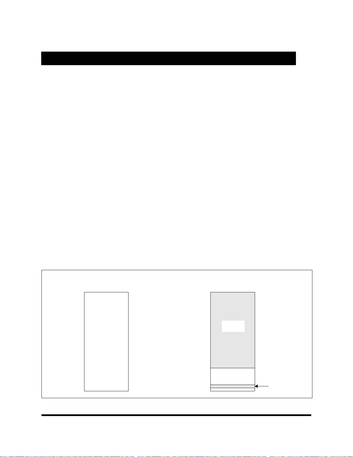
3.4 Address Spaces
The MediaGX processor can directly address
either memory or I/O space. Figure 3-2 illustrates
the range of addresses available for memory
address space and I/O address space. For the
CPU, the addr esses for physical memory range
between 00000000h and FFFFFFFFh
(4 GBytes). The accessible I/O addre sses spa ce
ranges between 00000000h and 0000FFFFh
(64KB). The CPU does not use coprocessor
communication space in upper I/O space between
800000F8h and 800000FFh as do the 386-style
CPUs. The I/O locations 22h and 23h are used for
MediaGX processor configuration register access.
3.4.1 I/O Address Space
The CPU I/O address space is accessed using IN
and OUT instructions to addresses referred to as
“ports.” The accessible I/O address space is 64KB
and can be accessed as 8-bit, 16-bit or 32-bit
ports.
The MediaGX processor configuration registers
reside within the I/O address space at port
Address Spaces
3
addresses 22h and 23h and are accessed using
the standard IN and OUT instructions.
The configuration registers are modifi ed by writi ng
the index of the configuration register to port 22h,
and then transferring the data through port 23h.
Accesses to the on-chip configuration registers do
not generate external I/O cycles. However, each
operation on port 23h must be preceded by a write
to port 22h with a valid index value. Otherwise,
subsequent port 23h operations will communicate
through the I/O port t o produce external I/O cycles
without modifying the on-chip co nfigur ati on regis -
ters. Write operations to port 22h outside of the
CPU index range (C0h-CFh and FEh-FFh) result in
external I/O cycles and do not affect the on-chip
configuration registers. Reading port 22h gener-
ates external I/O cycles.
I/O accesses to port address range 3B0h through
3DFh can be trapped to SMI by the CPU if this
option is enabled in the BC_XMAP_1 register (see
SMIB, SMIC, and SMID bits in Table 4-9 on page
113). Figure 3-2 illustrates the I/O address space.
Accessible
Programmed
I/O Space
Not
Accessible
64KB
CPU General
Configuration
Register I/O
Space
0000 0023h
0000 0022h
FFFF FFFFh
0000 0000h
Physical
Memory Space
FFFF FFFFh
Physical Memory
4GB
0000 FFFFh
0000 0000h
Figure 3-2 Memory and I/O Address Spaces
GXm_db_v2.0 Cyrix Corporation Confidential Page 65
Page 82

Offset, Segment, and Paging Mechanisms
3.4.2 Memory Address Space
The processor directly addresses up to 4GB of
physical memory even though the memory
controller addresses only 128MB of DRAM. Much
of the other 4GB can be on PCI. Memory address
space is accessed as bytes, words (16 bits) or
DWORDs (32 bits). Words and DWORDs are
stored in consecutive memory bytes with the loworder byte located in the lowest address. The physical address of a word or DWORD is the byte
address of the low-order byte.
The processor allows memory to be addressed
using nine different addressing modes. These
addressing modes are used to calculate an offset
address, often referred to as an effective address.
Depending on the operating mode of the CPU, the
offset is then combined, using memory management mechanisms, into a physical address that is
applied to the physical memory devices.
Memory management mechanisms consist of
segmentation and paging. Segmentation allows
each program to use several independent,
protected address spaces. Paging translates a
logical address into a physical address using translation lookup tables. Virtual memory is often implemented using paging. Either or both of these
mechanisms can be used for management of the
MediaGX processor memory address space.
3.5 Offset, Segment, and Paging
Mechanisms
The mapping of address space into a sequence of
memory locations (often cached) is performed by
the offset, segment and paging mechanisms.
In general, the offset, segment and paging mechanisms work in tandem as shown below:
instruction offset ➾
offset address
linear address ➾
As will be explained, the actual operations depend
on several factors such as the current operating
mode and if paging is enabled. Note: the paging
mechanism uses part of the linear address as an
offset on the physical page.
offset mechanism
segment mechanism
➾
paging mechanism
offset address
➾
➾ linear address
➾ physical page.
Page 66 Cyrix Corporation Confidential GXm_db_v2.0
Page 83
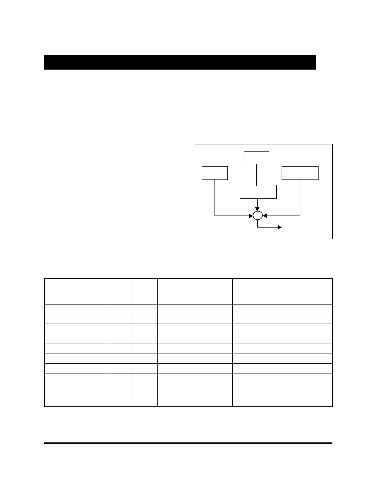
Offset Mechanism
3
3.6 Offset Mechanism
In all operating modes, the offset mechanism
computes an offset (effective) address by adding
together up to three values: a base, an index and a
displacement. The base, if present, is the value in
one of eight general registers at the time of the
execution of the instruction. The index, like the
base, is a value that is contained in one of the
general registers (except the ESP register) when
the instruction is executed. The index differs from
the base in that the index is first multiplied by a
scale factor of 1, 2, 4 or 8 before the summation is
made. The third component added to the memory
address calculation is the displacement that is a
value supplied as part of the instruction. Figure 3-3
illustrates the calculation of the offset address.
Nine valid combinations of the base, index, scale
factor and displacement can be used with the CPU
instruction set. These combinations are listed in
Table 3-18. The base and index both refer to
contents of a register as indicated by [Base] and
[Index].
In real mode operation, the CPU only addresses
the lowest 1MB of memory and the offset contains
16-bits. In protective mode the offset contains 32
bits. Initialization and transition to protective mode
is described in Section 3.13.4 “Initialization and
Transition to Protected Mode” on page 99.
Index
Base
Scaling
x1, x2, x4, x8
+
Displacement
Offset Address
(Effective Address)
Figure 3-3 Offset Address Calculation
Table 3-18 Memory Addressing Modes
Scale
Factor
Addressing Mode Base Index
Direct x OA = DP
Register Indirect x OA = [BASE]
Based x x OA = [BASE] + DP
Index x x OA = [INDEX] + DP
Scaled Index x x x OA = ([INDEX] * SF) + DP
Based Index x x OA = [BASE] + [INDEX]
Based Scaled Index x x x OA = [BASE] + ([INDEX] * SF)
Based Index with
Displacement
Based Scaled Index
with Displacement
x x x OA = [BASE] + [INDEX] + DP
x x x x OA = [BASE] + ([INDEX] * SF) + DP
(SF)
Displacement
(DP)
Offset Address (OA)
Calculation
GXm_db_v2.0 Cyrix Corporation Confidential Page 67
Page 84
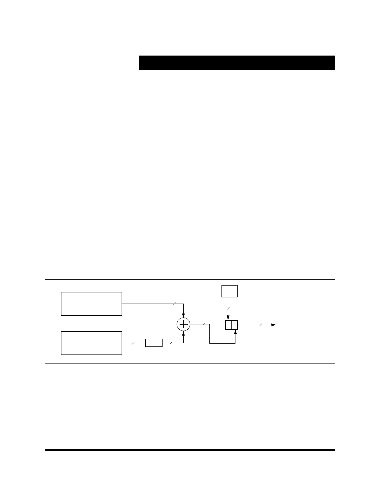
Descriptors and Segment Mechanisms
3.7 Descriptors and Segment
Mechanisms
Memory is divided into contiguous regions called
“segments.” The segments allow the partitioning of
individual elements of a program. Each segment
provides a zero address-based private memory for
such elements as code, data and stack space.
The segment mechanisms select a segment in
memory. Memory is divided into an arbitrary
number of segments, each containing usually
much less than the 2
There are two segment mechanisms, one for Real
and Virtual 8086 Operating Modes, and one for
Protective Mode.
32
byte (4 GByte) maximum.
3.7.1 Real and Virtual 8086 Mode
Segment Mechanisms
Real Mode Segment Mechanism
In real mode operation, the CPU addresses only
the lowest 1MB of memory. In this mode a selector
located in a one of the segment registers is used to
locate a segment.
To calculate a physical memory address, the 16-bit
segment base address located in the selected
segment register is multiplied by 16 and then a 16bit offset address is added. The resulting 20-bit
address is then extended with twelve zeros in the
upper address bits to crate 32-bit physical address.
The value of the selector (the INDEX field) is multiplied by 16 to produce a base address (Figure 3 - 4. )
The base address is summed with the instruction
offset value to produce a physical address.
Virtual 8086 Mode Segment Mechanism
In Virtual 8086 mode the operation is performed as
in real mode except that a paging mechanism is
added. When paging is enabled, the paging
mechanism translates the linear address into a
physical address using cached look-up tables
(refer to Section 3.9 “Paging Mechanism” on page
80).
12 High Order Address Bits
000h
Offset Mechanism
Selected Segment
Register
Page 68 Cyrix Corporation Confidential GXm_db_v2.0
Offset Address
16
X 16
Figure 3-4 Real Mode Address Calculation
16
20
Base Address
12
20
32
(Physical Address)
Linear Address
Page 85
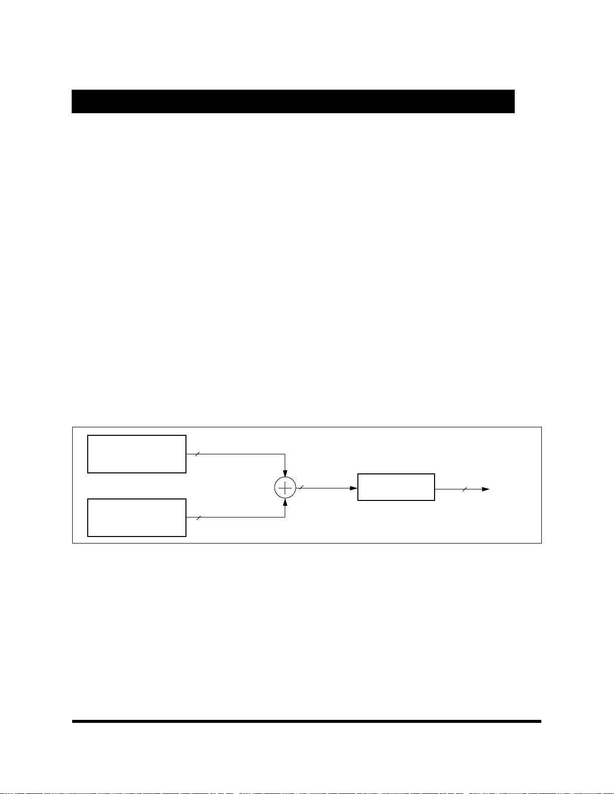
Descriptors and Segment Mechanisms
3
3.7.2 Segment Mechanism in
Protective Mode
The segment mechanism in protective mode is
more complex. Basically as in Real and Virtual
8086 modes the offset address is added to the
segment base address to produce a linear address
(Figure 3-5). However, the calculation of the
segment base address is based on the contents of
descriptor tables.
Again, if paging is enabled the linear address is
further processed by the paging mechanism.
A more detailed look at the segment mechanisms
for real, virtual 8086 and protective modes is illustrated in Figure 3-6. In protective mode, the
segment selector is cached. This is illustrated in
Figure 3-7 on page 71.
3.7.2.1 Segment Selectors
The segment registers are used to store segment
selectors. In protective mode, the segment
selectors are divided in to three fields: the RPL, TI
and INDEX fields as shown in Figure 3-6.
The segments are assigned permission le vels to
prevent applicat ion p rogra m e r ror s f rom dis ru pt ing
opera ti ng p ro gra ms . The Requested Privilege Level
(RPL) determines the E ffective Privilege L evel of a n
instruction. RPL = 0 indicates th e most privileg ed
level, and RPL = 3 indicates the least privileged level.
Refer to Section 3.13 “Protection” on page 97.
Descriptor tables hold descriptors that allow
management of segments and tables in address
space while in protective mode. The Table Indicator Bit (TI) in the selector selects either the
General Descriptor Table (GDT) or one Local
Descriptor Tables (LDT) tables. If TI = 0, GDT is
selected; if TI =1, LDT is selected. The 13-bit
INDEX field in the segment selector is used to
index a GDT or LDT table.
Offset Mechanism
Selector Mechanism
32
Offset Address
Linear
Segment Base
32
Address
32
Address
Optional
Paging Mechanism
Figure 3-5 Protected Mode Address Calculation
32
Physical
Memory
Address
GXm_db_v2.0 Cyrix Corporation Confidential Page 69
Page 86
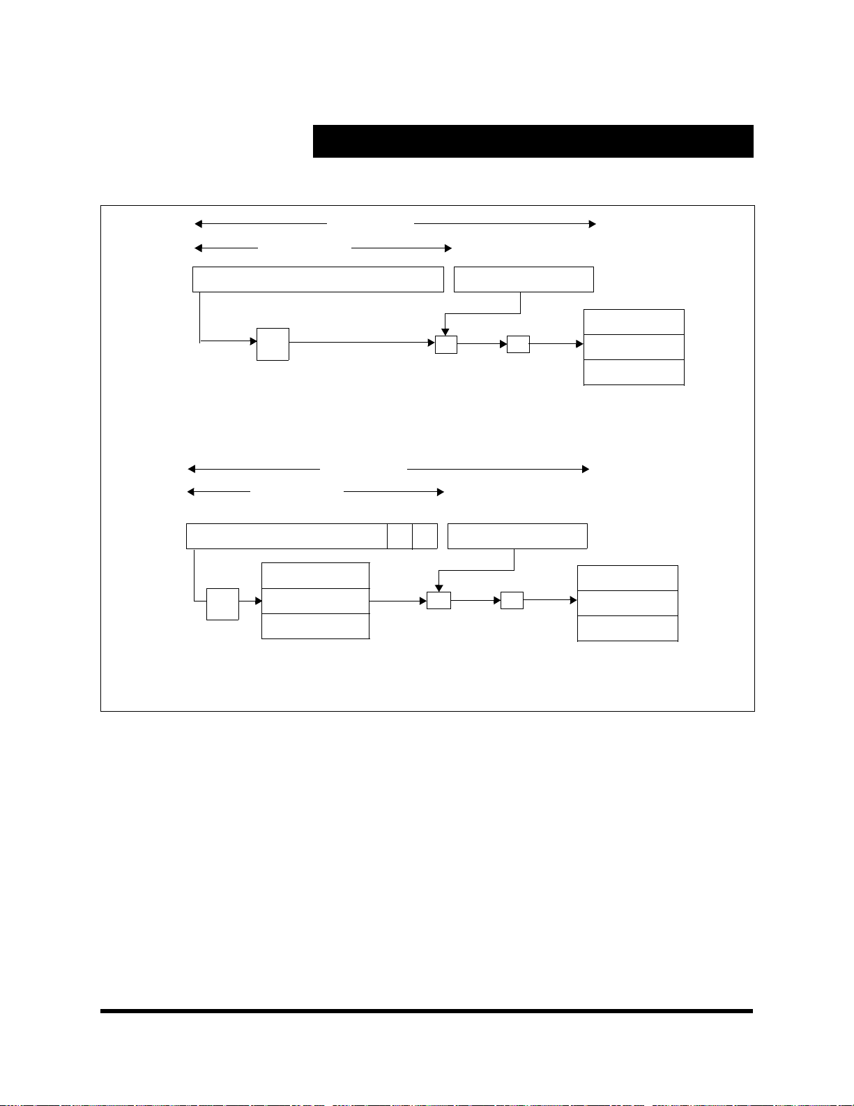
g
g
g
g
Descriptors and Segment Mechanisms
ical Address
Lo
15 0
Lo
Address
p= Paging Mechanism for Virtual 8086 Mode only
15 3 2 1 0
x 8
Segment Selector
INDEX
ical
x 16
Lo
Se
ment Selector
INDEX TI
Segment Descriptor
GDT or LDT Descriptor Table
Base
Address
Real and Virtual 8086 Modes
ical Address
RPL
Base
Address
INSTRUCTION OFFSET
+
Linear
Address
INSTRUCTION OFFSET
+
Linear
Address
p = Paging Mechanism
p
p
Physical
Address
Physical
Address
Segment
Main Memory
Segment
Main Memory
Protective Mode
Figure 3-6 Selector Mechanisms
Page 70 Cyrix Corporation Confidential GXm_db_v2.0
Page 87
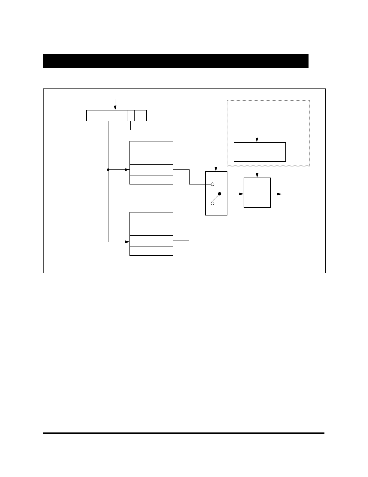
Selector Load Instruction
g
g
g
g
Descriptors and Segment Mechanisms
3
In Se
Selector
ment
ister
Re
15 0
INDEX TI RPL
Segment
Descriptor
Global Descriptor
Segment
Descriptor
Local Descriptor
Table
Table
TI = 0
TI = 1
Segment Register
Selected By Decoded
Instruction
Cached Segment
and Descriptor
Cached
Selector
Used If
Available
Se
ment
Cachin
Segment
Base
Address
Figure 3-7 Selector Mechanism Caching
GXm_db_v2.0 Cyrix Corporation Confidential Page 71
Page 88
Descriptors and Segment Mechanisms
3.7.3 GDTR and LDTR Registers
The GDT, and LDT descriptor tables are defined by
the Global Descriptor Table Register (GDTR) and
the Local Descriptor Table Register (LDTR) respectively. Some texts refer to these registers as GDT,
and LDT descriptors.
The following instructions are used in conjunction
with the GDTR and LDTR registers:
• LGDT - Load memory to GDTR
• LLDT - Load memory to LDTR
• SGDT - Store GDTR to memory
• SLDT - Store LDTR to memory
The GDTR is set up in REAL mode using the
LGDT instruction. This is possible as the LGDT
instructions are one of two instructions that directly
load a linear address (instead of a segment relative
address) in protective mode. (The other instruction
is the Load Interrupt Descriptor Table [LIDT]).
As shown in Table 3-19, the GDTR registers
contain a BASE ADDRESS field and a LIMIT field
to that define the GDT tables. (The IDTR register is
described in Section 3.7.3.2 “Task, Gate and Interrupt Descriptors” on page 73.)
Also shown in Table 3-19, the LDTR is only two
bytes wide as it contains only a SELECTOR field.
The contents of the SELECTOR field points to a
descriptor in the GDT table.
3.7.3.1 Segment Descript o rs
There are several types of descriptors. A segment
descriptor defines the base address, limit and
attributes of a memory segment.
The GDT or LDT table can hold several types of
descriptors. In particular, the segment descriptors
are stored in either of two registers, the GDT , or the
LDT as shown in Table 3-19). Either of these tables
can store as many as 8,192 (2
tors taking as much as 64KB of memory.
The first descriptor in the GDT (location 0) is not
used by the CPU and is referred to as the “null
descriptor.”
Types of Segment Descriptors
The type of memory segments are defined as
defined by corresponding types of segment
descriptors:
• Code Segment Descriptors
• Data Segment Descriptors
• Stack Segment Descriptors
• LDT Segment Descriptors
13
) eight-byte selec-
Table 3-19 GDTR, LDTR and IDTR Registers
47 161514131211109876543210
GDTR Register
BASE LIMIT
IDTR Register
BASE LIMIT
LDTR Register
SELECTOR
Page 72 Cyrix Corporation Confidential GXm_db_v2.0
Page 89
Descriptors and Segment Mechanisms
3
3.7.3.2 Task, Gate and Interrupt
Descriptors
Besides segment descriptors there are descriptors
used in task switching, switching between tasks
with different priority and those used to control
interrupt functions:
• Task State Segment Table Descriptors
• Gate Table Descriptor s
• Interrupt Descriptors.
All descriptors some things in common. They are
all eight bytes in length and have three fields in
(BASE, LIMIT and TYPE). The BASE field defines
the starting location for the table or segment. The
LIMIT field defines the size and the TYPE field
depends on the type of descriptor. One of the main
functions of the TYPE field is to define the access
rights to the associated segment or table.
Interrupt Descriptor Table
The Interrupt Descriptor Table is an array of 256 8byte (4-byte for real mode) interrupt descriptors,
each of which is used to point to an interrupt
service routine. Every interrupt that may occur in
the system must have an associated entry in the
IDT. The contents of the IDTR are completely
visible to the programmer through the use of the
SIDT instruction.
The IDT descriptor table is defined by the Interrupt
Descriptor Table Register (IDTR). Some texts refer
to this register as an IDT descriptor.
The following instructions are used in conjunction
with the IDTR registers:
• LIDT - Load memory to IDTR
• SIDT - Store IDTR to memory
The IDTR is set up in REAL mode using the LIDT
instruction. This is possible as the LIDT instructions is only one of two instructions that directly
load a linear address (instead of a segment relative
address) in protective mode.
As previously shown in Table 3-19, the IDTR
register contains a BASE ADDRESS field and a
LIMIT field that define the IDT tables.
3.7.4 Descriptor Bit Structure
The bit structure for application and system
descriptors is shown in Table 3-20. The explanation of the TYPE field is shown in Table 3-22.
Table 3-20 Application and System Segment Descriptors
31312928272625242322212019181716151413121110987654321 0
Memory Offset +4
BASE[31:24] G D 0 A
Memory Offset +0
BASE[15:0] LIMIT[15:0]
GXm_db_v2.0 Cyrix Corporation Confidential Page 73
LIMIT[19:16] P DPL S TYPE BASE[23:16]
V
L
Page 90
Descriptors and Segment Mechanisms
g
g
g
g
g
g
g
g
g
g
g
g
g
g
g
g
g
g
Table 3-21 Application and System Segment Descriptors Bit Definitions
Memory
Bit
31:24 +4 BASE
7:0 +4
31:16 +0
19:16 +4 LIMIT
15:0 +0
14:13 +4 DPL
11:8 +4 TYPE Se
Offset Nam e Description
23 +4 G
22 +4 D
20 +4 AVL
15 +4 P
12 +4 S
Segment Base Address:
in 4GB physical address space.
Segment Limit:
Granularity Bit.
If G = 1: Limit value interpreted in units of 4KB.
If G = 0: Limit value is interpreted in bytes.
Segment Limit Granularity Bit:
If G = 1: Limit value interpreted in units of 4KB. Se
If G = 0: Limit value is interpreted in bytes. Se
Default Length for Operands and Effective Addresses:
If D = 1: Code se
If D = 0: Code se
If D = 1: Data se
If D = 0: Data se
Segment Available:
Segment Present:
If = 1: Se
If = 0: The BASE and LIMIT fields become available for use by the system. Also, If = 0, a se
not-present exception
virtual memory management.
allowin
Descriptor Privilege Level:
If = 00: Hi
If = 11: Low privile
Descriptor Type:
If = 1: Code or data se
If = 0: System se
ment Type - Refer to Table 3-22 for TYPE bit definitions.
Bit 11 = Executable
Bit 10 = Conformin
Bit 10 = Expand Down if bit 12 = 0
Bit 9 = Readable, if Bit 12 = 1
Bit 9 = Writable, if Bit 12 = 0
Bit 8 = Accessed
Two fields that define the size of the se
ment is memory segment allocated.
hest privilege level
Three fields which collectively define the base location for the se
ment based on the Segment Limit
Defines LIMIT multiplier.
ment size ranges from 1 byte to 1MB.
ment size ranges from 4KB to 4GB.
ment = 32-bit length for operands and effective addresses
ment = 16-bit length for operands and effective addresses
ment = Pushes, calls and pop instructions use 32-bit ESP register
ment = Stack operations use 16-bit SP register
This field is available for use by system software.
enerated when selector for the descriptor is loaded into a segment register
e level
ment
ment
if bit 12 = 1
ment
ment-
Page 74 Cyrix Corporation Confidential GXm_db_v2.0
Page 91
Descriptors and Segment Mechanisms
g
g
g
g
g
g
Table 3-22 Application and System Segment Descriptors TYPE Bit Definitions
TYPE
Bits [11:8]
Num SEWA TYPE (Data Se
0 0000 Reserved Data Read-Only
1 0001 Available 16-Bit TSS Data Read-Only, accessed
2 0010 LDT Data Read/Write
3 0011 Busy 16-Bit TSS Data Read/Write accessed
4 0100 16-Bit Call Gate Data Read-Only, expand down
5 0101 Task Gate Data Read-Only, expand down, accessed
6 0110 16-Bit Interrupt Gate Data Read/Write, expand down
7 0111 16-Bit Trap Gate Data Read/Write, expand down, accessed
Num SCRA TYPE (Code Se
8 1000 Reserved Code Execute-Only
9 1001 Available 32-Bit TSS Code Execute-Only, accessed
A 1010 Reserved Code Execute/Read
B 1011 Busy 32-Bit TSS Code Execute/Read, accessed
C 1100 32-Bit Call Gate Code Execute/Read, conformin
D 1 101 Reserved Code Execute/Read, conforming, accessed
E 1110 32-Bit Interrupt Gate Code Execute/Read-Only, conformin
F 1111 32- Bit Trap G ate Code Execute/Read-Only, conforming accessed
S = Code Se
E = Expand Down
W = Write Enable
ment (not Data Segment)
System Segment and Gate Types
Bit 12 = 0
ments)
ments)
Application Segment Types
A = Accessed
C = Conformin
R = Read Enable
Bit 12 = 1
Code Segment
3
GXm_db_v2.0 Cyrix Corporation Confidential Page 75
Page 92
Descriptors and Segment Mechanisms
3.7.5 Gate Descriptors
Four kinds of gate descriptors are used to provide
protection during control transfers: call gates, trap
gates, interrupt gates and task gates. (For more
information on protection refer to Section 3.13
“Protection” on page 97.)
Call Gate Descriptor (CGD).
to define legal entry points to a procedure with a
higher privilege level. The call gates are used by
CALL and JUMP instructions in much the same
manner as code segment descriptors. When the
CPU decodes an instruction and sees it refers to a
call gate descriptor in the GDT table or a LDT
table, the call gate is used to point to another
descriptor in the table that defines the destination
code segment.
The following privilege levels are tested during the
transfer through the call gate:
• CPL = Current Privilege Level
Call gates are used
• RPL = Segment Selector Field
• DPL = Descriptor Privilege Level in the call gate
descriptor.
• DPL = Descriptor Privilege Level in the destination code segment.
The maximum value of the CPL and RPL must be
equal or less than the gate DPL. For a JMP
instruction the destination DPL equals the CPL.
For a CALL instruction the destination DPL is less
or equals the CPL.
Conforming Code Segments.
Transfer to a
procedure with a higher privilege level can also be
accomplished by bypassing the use of call gates, if
the requested procedure is to be executed in a
conforming code segment. Conforming code
segments have the C bit set in the TYPE field in
their descriptor.
The bit structure and definitions for gate descriptors are shown in Tables 3-23 and 3-24.
Table 3-23 Gate Descriptors
313029282726252423222120191817161514131211109876543210
Memory Offset +4
OFFSET[31:16] P DPL 0 TYPE 0 0 0 PARAMETERS
Memory Offset +0
SELECTOR[15:0] OFFSET[15:0]
Table 3-24 Gate Descriptors Bit Definitions
Bit
31:16 +4 OFFSET
15:0 +0
31:16 +0 SELECTOR
15 +4 P
14:13 +4 DPL
11:8 +4 TYPE
4:0 +4 PARAMETERS
Page 76 Cyrix Corporation Confidential GXm_db_v2.0
Memory
Offset Name Description
Offset used during a call gate to calculate the branch target.
Offset:
Segment Selector
Segment Present
Descriptor Privilege Level
Segment Type:
0100 = 16-bit call gate 1100 = 32-bit call gate
0101 = Task gate 1110 = 32-bit interrupt gate
0110 = 16-bit interrupt gate 1111 = 32-bit trap gate
0111 = 16-bit trap gate
Parameters
dure’s stack.
: Number of parameters to copy from the caller’s stack to the called proce-
Page 93

Multitasking and Task State Segments
3
3.8 Multitasking and Task State
Segments
The CPU enables rapid task switching using JMP
and CALL instructions that refer to Task State
Segments (TSS). During a switch, the complete
task state of the current task is stored in its TSS,
and the task state of the requested task is loaded
from its TSS. The TSSs are defined through
special segment descriptors and gates.
The
Task Register (TR)
that contain the base address and segment limit for
each task state segment. The TR is loaded and
stored via the LTR and STR instructions, respectively. The TR can only be accessed only during
protected mode and can be loaded when the privilege level is 0 (most privileged). When the TR is
loaded, the TR selector field indexes a TSS
descriptor that must reside in the Global Descriptor
Table (GDT).
holds 16-bit descriptors
Only the 16-bit selector of a TSS descriptor in the
TR is accessible. The BASE, TSS LIMT and
ACCESS RIGHT fields are program invisible.
During task switching, the processor saves the
current CPU state in the TSS before starting a new
task. The TSS can be either a 386/486-type 32-bit
TSS (see Table 3-25) or a 286-type 16-bit TSS (see
Table 3-26).
T ask Gate Descriptors.
provides controlled access to the descriptor for a
task switch. The DPL of the task gate is used to
control access. The selector’s RPL and the CPL of
the procedure must be a higher level (numerically
less) than the DPL of the descriptor. The RPL in
the task gate is not used.
The I/O Map Base Address field in the 32-bit TSS
points to an I/O permission bit map that often
follows the TSS at location +68h.
A task gate descriptor
GXm_db_v2.0 Cyrix Corporation Confidential Page 77
Page 94
Multitasking and Task State Segments
Table 3-25 32-Bit Task State Segment (TSS) Table
31 16 15 0
I/O Map Base Address 000000000000000T +64h
0000000000000000 Selector for Task’s LDT +60h
0000000000000000 GS +5Ch
0000000000000000 FS +58h
0000000000000000 DS +54h
0000000000000000 SS +50h
0000000000000000 CS +4Ch
0000000000000000 ES +48h
EDI +44h
ESI +40h
EBP +3Ch
ESP +38h
EBX +34h
EDX +30h
ECX +2Ch
EAX +28h
EFLAGS +24h
EIP +20h
CR3 +1Ch
0000000000000000 SS for CPL = 2 +18h
ESP for CPL = 2 +14h
0000000000000000 SS for CPL = 1 +10h
ESP for CPL = 1 +Ch
0000000000000000 SS for CPL = 0 +8h
ESP for CPL = 0 +4h
0000000000000000 Back Link (Old TSS Selector) +0h
Note:
0 = Reserved
Page 78 Cyrix Corporation Confidential GXm_db_v2.0
Page 95

Multitasking and Task State Segments
g
g
g
g
g
g
Table 3-26 16-Bit Task State Segment (TSS) Table
15 0
Selector for Task’s LDT +2Ah
DS +28h
SS +26h
CS +24h
ES +22h
DI +20h
SI +1Eh
BP +1Ch
SP +1Ah
BX +18h
DX +16h
CX +14h
AX +12h
FLAGS +10h
IP +Eh
SS for Privile
SP for Privile
SS for Privile
SP for Privile
SS for Privile
SP for Privile
Back Link (Old TSS Selector) +0h
e Level 0 +Ch
e Level 1 +Ah
e Level 1 +8h
e Level 1 +6h
e Level 0 +4h
e Level 0 +2h
3
GXm_db_v2.0 Cyrix Corporation Confidential Page 79
Page 96
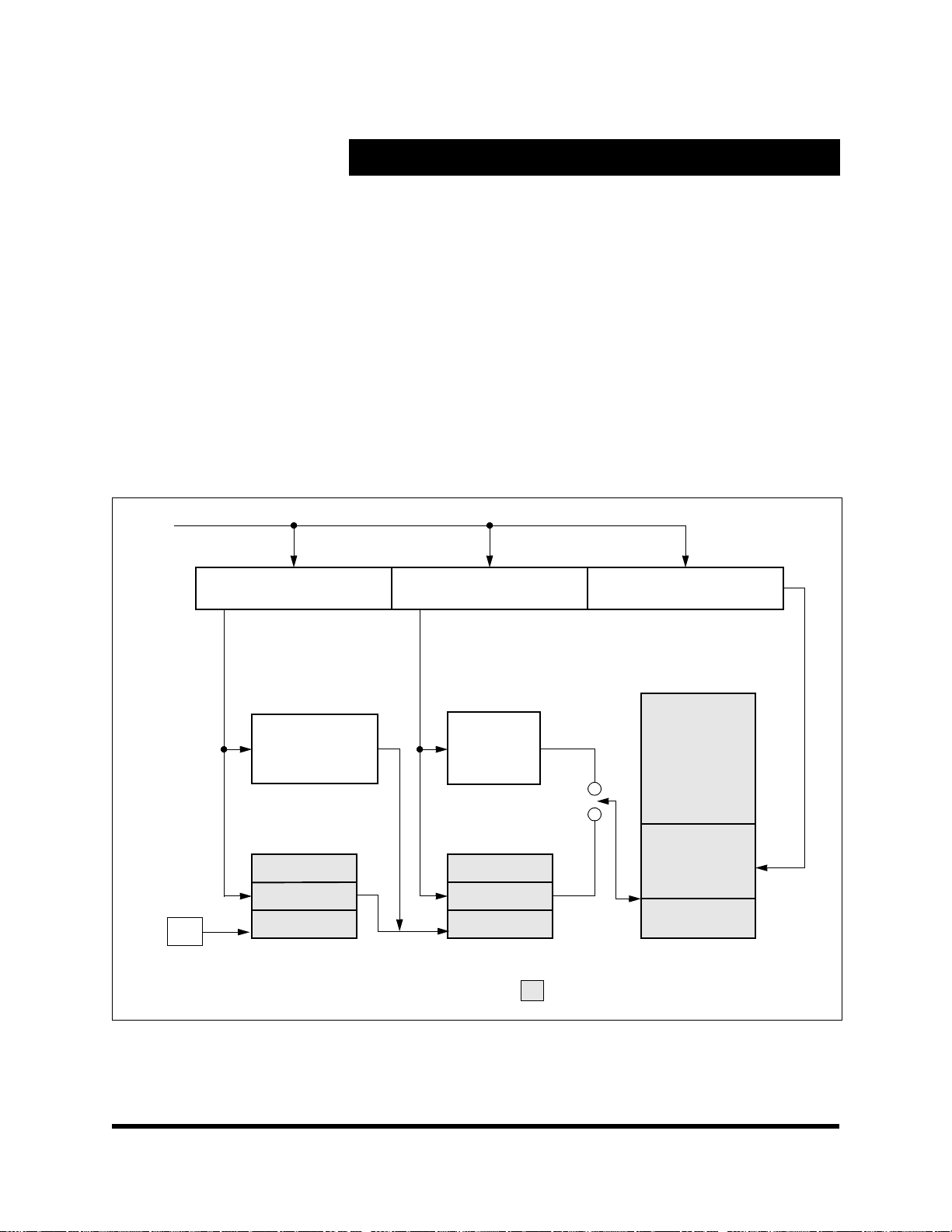
Paging Mechanism
3.9 Paging Mechanism
The paging mechanism either translates a linear
address to its corresponding physical address. If
the required page is not currently present in RAM,
an exception is generated. When the operating
system services the exception, the required page
can be loaded into memory and the instru ct io n
restarted. Pages are either 4KB or 1MB in size.
The CPU defaults to 4KB pages that are aligned to
4KB boundaries.
A page is addressed by using two levels of tables
as illustrated in Figure 3-8. Bits[31:22] of the 32-bit
linear address, the Directory Table Index (DTI) are
Linear
Address
31 22 21 12 11 0
Directory Table Index
(DTI)
Page Table Index
used to locate an entry in the page directory table.
The page directory table acts as a 32-bit master
index to up to 1K individual second-level page
tables. The selected entry in the page directory
table, ref erred to as the dire ctory tabl e entry (D TE),
identifies the starting address of the second-level
page table. The page directory table itself is a page
and is, therefore, aligned to a 4KB boundary. The
physical address of the current page directory table
is stored in the CR3 control register, also referred
to as the Page Directory Base Register (PDBR).
(PTI)
Page Frame Offset
(PFO)
CR3
Control
Register
DTE Cache
2-Entry
Fully Associative
DTE
Directory Table Page Table Memory
1
0
4KB
0
Figure 3-8 Paging Mechanism
Main TLB
32-Entry
4-Way Set
Associative
PTE
31
0
4KB
0
External Memory
Physical Page
4GB
-4KB
-0
0
Page 80 Cyrix Corporation Confidential GXm_db_v2.0
Page 97
Paging Mechanism
3
Bits [21:12] of the 32-bit linear address, referred to
as the Page Table Index (PTI), locate a 32-bit entry
in the second-level page table. This Page Table
Entry (PTE) contains the base address of the
desired page frame. The second-level page table
addresses up to 1K individual page frames. A
second-level page table is 4KB in size and is itself
a page. Bits [11:0] of the 32-bit linear address, the
Page Frame Offset (PFO), locate the desired physical data within the page frame.
Since the page directory table can point to 1K page
tables, and each page table can point to 1K page
frames, a total of 1M page frames can be implemented. Since each page frame contains 4KB, up
to 4GB of virtual memory can be addressed by the
CPU with a single page directory table.
If the present bit (P) is set in the DTE, the page
table is present and the appropriate page table
entry is read. If P = 1 in the corresponding PTE
(indicating that the page is in memory), the
accessed and dirty bits are updated, if necessary,
and the operand is fetched. Both accessed bits are
set (DTE and PTE), if necessary, to indicate that
the table and the page have been used to translate
a linear address. The dirty bit (D) is set before the first
write is made to a page.
The present bits must be set to validate the
remaining bits in the DTE and PTE. If either of the
present bits are not set, a page fault is generated
when the DTE or PTE is accessed. If P = 0, the
remaining DTE/PTE bits are available for use by
the operating system. For example, the operating
system can use these bits to record where on the
Along with the base address of the page table or
the page frame, each directory table entry or page
table entry contains attribute bits and a present bit
hard disk the pages are located. A page fault is
also generated if the memory reference violates
the page protection attributes.
as illustrated in Table 3-27.
Table 3-27 Directory Table Entry (DTE) and Page Table Entry (PTE)
Bit Name Description
31:12 BASE
ADDRESS
11:9 AVAILABLE
8:7 RSVD
6D
5A
4:3 RSVD
2U/S
1W/R
0P
Base Address:
Available:
Reserved:
Dirty Bit:
PTE format — If = 1: Indicates that a write access has occurred to the page.
DTE format — Reserved.
Accessed Flag:
Reserved:
User/Supervisor Attribute:
If = 1: Page is accessible by User at privilege level 3.
If = 0: Page is accessible by Supervisor only when CPL ≤ 2.
Write/Read Attribute:
If = 1: Page is writable.
If = 0: Page is read only.
Present Flag:
If = 1: The page is present in RAM and the remaining DTE/PTE bits are validated
If = 0: The page is not present in RAM and the remaining DTE/PTE bits are available for use by the
programmer.
Specifies the base address of the page or page table.
Undefined and Available to the Programmer
Unavailable to programmer
If set, indicates that a read access or write access has occurred to the page.
Set to 0.
GXm_db_v2.0 Cyrix Corporation Confidential Page 81
Page 98

Interrupts and Exceptions
Translation Look-Aside Buffer
The translation look-aside buffer (TLB) is a cache
for the paging mechanism and replaces the twolevel page table lookup procedure for TLB hits. The
TLB is a four-way set associative 32-entry page
table cache that automatically keeps the most
commonly used page table entries in the
processor. The 32-entry TLB, coupled with a 4K
page size, results in coverage of 128KB of memory
addresses.
The TLB must be flushed when entries in the page
tables are changed. The TLB is flushed whenever
the CR3 register is loaded. An individual entry in
the TLB can be flushed using the INVLPG instruction.
DTE Cache
The DTE cache caches the two most recent DTEs
so that future TLB misses only require a single
page table read to calculate the physical address.
The DTE cache is disabled following reset and can
be enabled by setting the DTE_EN bit in CCR4[4]
(Index E8h).
3.10 Interrupts and Exceptions
The processing of either an interrupt or an exception changes the normal sequential flow of a
program by transferring program control to a
selected service routine. Except for SMM interrupts, the location of the selected service routine is
determined by one of the interrupt vectors stored in
the interrupt descriptor table.
True interrupts are hardware interrupts and are
generated by signal sources external to the CPU.
All exceptions (including so-called software interrupts)
are produced internally by the CPU.
3.10.1 Interrupts
External events can interrupt normal program
execution by using one of the three interrupt pins
on the MediaGX processor:
• Non-maskable Interrupt (NMI pin)
• Maskable Interrupt (INTR pin)
• SMM Interrupt (SMI# pin)
For most interrupts, program transfer to the inter-
rupt routine occurs after the current instruction has
been completed. When the execution returns to the
original program, it begins immediately following
the interrupted instruction.
The
NMI interrupt
and always uses interrupt vector 2 to locate its
service routine. Since the interrupt vector is fixed
and is supplied internally , no interrupt acknowledge
bus cycles are performed. This interrupt is normally
reserved for unusual situations such as parity
errors and has priority over INTR interrupts.
Once NMI processing has started, no additional
NMIs are processed until an IRET instruction is
executed, typically at the end of the NMI service
routine. If NMI is re-asserted before execution of
the IRET instruction, one and only one NMI rising
edge is stored and then processed after execution
of the next IRET.
During the NMI service routine, maskable interrupts may be enabled. If an unmasked INTR
occurs during the NMI service routine, the INTR is
serviced and execution returns to the NMI service
routine following the next IRET. If a HAL T instruction is executed within the NMI service routine, the
CPU restarts execution only in response to
RESET, an unmasked INTR or a System Management Mode (SMM) interrupt. NMI does not restart
CPU execution under this condition.
cannot be masked by software
The
INTR interrupt
rupt Enable Flag (IF, bit 9) in the EFLAGS register
is set to 1. Except for string operations, INTR interrupts are acknowledged between instructions.
Long string operations have interrupt windows
Page 82 Cyrix Corporation Confidential GXm_db_v2.0
is unmasked when the Inter-
between memory moves that allow INTR interrupts
to be acknowledged.
When an INTR interrupt occurs, the CPU performs
an interrupt-acknowledge bus cycle. During this
cycle, the CPU reads an 8-bit vector that is
supplied by an external interrupt controller. This
Page 99

Interrupts and Exceptions
3
vector selects which of the 256 possible interrupt
handlers will be executed in response to the interrupt.
The
SMM interrupt
INTR or NMI. After SMI# is asserted, program
execution is passed to an SMI service routine that
runs in SMM address space reserved for this
purpose. The remainder of this section does not
apply to the SMM interrupts. SMM interrupts are
described in greater detail later in this section.
has higher priority than either
3.10.2 Exceptions
Exceptions are generated by an interrupt instruction or a program error. Exceptions are classified
as traps, faults or aborts depending on the mechanism used to report them and the restartability of
the instruction which first caused the exception.
A
Trap exception
following the instruction that generated the trap
exception. Trap exceptions are generated by
execution of a software interrupt instruction (INTO,
INT3, INTn, BOUND), by a single-step operation or
by a data breakpoint.
Software interrupts can be used to simulate hardware interrupts. For example, an INTn instruction
causes the processor to execute the interrupt
service routine pointed to by the nth vector in the
interrupt table. Execution of the interrupt service
routine occurs regardless of the state of the IF flag
(bit 9) in the EFLAGS register.
is reported immediately
A
Fault exception
the instruction that generated the exception. By
reporting the fault before instruction completion,
the CPU is left in a state that allows the instruction
to be restarted and the effects of the faulting
instruction to be nullified. Fault exceptions include
divide-by-zero errors, invalid opcodes, page faults
and coprocessor errors. Debug exceptions (vector
1) are also handled as faults (except for data
breakpoints and single- s tep oper at ion s). Afte r
execution of the fault service routine, the instruction pointer points to the instruction that caused the
fault.
An
Abort exception
that is severe enough that the CPU cannot restart
the program at the faulting instruction. The double
fault (vector 8) is the only abort exception that
occurs on the CPU.
is reported before completio n of
is a type of fault exception
3.10.3 Interrupt Vectors
When the CPU services an interrupt or exception,
the current program’s instruction pointer and flags
are pushed onto the stack to allow resumption of
execution of the interrupted program. In protected
mode, the processor also saves an error code for
some exceptions. Program control is then transferred to the interrupt handler (also called the interrupt service routine). Upon execution of an IRET at
the end of the service routine, program execution
resumes at the instruction pointer address saved
on the stack when the interrupt was serviced.
The one byte INT3, or breakpoint interrupt (vector
3), is a particular case of the INTn instruction. By
inserting this one byte instruction in a program, the
user can set breakpoints in the code that can be
used during debug.
Single-step operation is enabled by setting the TF
bit (bit 8) in the EFLAGS register. When TF is set,
the CPU generates a debug exception (vector 1)
after the execution of every instruction. Data breakpoints also generate a debug exception and are
specified by loading the debug registers (DR0DR7) with the appropriate values.
GXm_db_v2.0 Cyrix Corporation Confidential Page 83
3.10.3.1 Interrupt Vector Assignments
Each interrupt (except SMI#) and exception is
assigned one of 256 interrupt vector numbers as
shown in Table 3-28. The first 32 interrupt vector
assignments are defined or reserved. INT instructions acting as software interrupts may use any of
interrupt vecto rs, 0 th ro ug h 25 5.
The non-maskable hardware interrupt (NMI) is
assigned vector 2. Illegal opcodes including faulty
FPU instructions will cause an illegal opcode
exception, interrupt vector 6. NMI interrupts are
Page 100
Interrupts and Exceptions
enabled by setting bit 2 of the CCR7 register (Index
EBh[2] = 1, see Table 3-11 on page 54 for register
format).
In response to a maskable hardware interrupt
(INTR), the CPU issues interrupt acknowledge bus
cycles used to read the vector number from external
hardware. These vectors should be in the range 32
to 255 as vector s 0 t o 31 are predefined. In PCs,
vectors 8 through 15 are used.
3.10.3.2 Interrupt Descriptor Table
The interrupt vector number is used by the CPU to
locate an entry in the interrupt descriptor table
(IDT). In real mode, each IDT entry consists of a
four-byte far pointer to the beginning of the corresponding interrupt service routine. In protected
mode, each IDT entry is an 8-byte descriptor. The
Interrupt Descriptor Table Register (IDTR) specifies the beginning address and limit of the IDT.
Following reset, the IDTR contains a base address
of 0h with a limit of 3FFh.
The IDT can be located anywhere in physical
memory as determined by the IDTR register. The
IDT may contain different types of descriptors:
interrupt gates, trap gates and task gates. Interrupt
gates are used primarily to enter a hardware interrupt handler. Trap gates are generally used to
enter an exception handler or software interrupt
handler. If an interrupt gate is used, the Interrupt
Enable Flag (IF) in the EFLAGS register is cleared
before the interrupt handler is entered. Task gates
are used to make the transition to a new task.
Table 3-28 Interrupt Vector Assignments
Interrupt
Vector Function
7 Device not available Fault
8 Double fault Abort
9 Reserved
10 Invalid TSS Fault
11 Segment not present Fault
12 Stack fault Fault
13 General protection fault Trap/Fault
14 Page fault Fault
15 Reserved
16 FPU error Fault
17 Alignment check exception Fault
18:31 Reserved
32:55 Maskable hardware interrupts Trap
0:255 Programmed interrupt Trap
*Data breakpoints and single steps are traps. All
Note:
other debug exceptions are faults.
Exception
Type
Table 3-28 Interrupt Vector Assignments
Interrupt
Vector Function
0 Divide error Fault
1 Debug exception Trap/Fault*
2 NMI interrupt
3 Breakpoint Trap
4 Interrupt on overflow Trap
5 BOUND range exceeded Fault
6 Invalid opcode Fault
Page 84 Cyrix Corporation Confidential GXm_db_v2.0
Exception
Type
 Loading...