

Page 1

PSoCEval User Guide
and Example Projects
Cypress MicroSystems, Inc.
2700 162nd Street SW, Building D
Lynnwood, WA 98037
Phone: 800.669.0557
Fax: 425.787.4641
1
Page 2

2
3
TABLE OF CONTENTS
INTRODUCTION TO PSOCEVAL
Introduction to the PsoCEval.....................................3
What Comes with my PSoCEval? .............................4
PSoCEval Power Supply Options..............................6
Introduction to MiniProg ...........................................7
Specications for MiniProg ....................................... 9
Operating Changes to the PsoCEval..........................9
Introduction to Example Projects.............................10
Example #1 ADC Conversion and LCD Display ......................11
Example #2 Blink an LED.........................................................16
Example #3 Output a SINE Wave..............................................19
Example #4 Dynamically Re-congure a PWM .......................24
Example #5 Combine PWMs using Output Logic ....................29
Cypress Support.......................................................32
Welcome to the new exciting world of the PSoCEval!
PSoCEval allows you to evaluate what PSoC has to offer. The
board includes an LCD module, potentiometer, LEDs, and plenty
of breadboard space. This user guide includes ve different
example projects that can be used with the PSoCEval board. The
MiniProg can program both the PSoC on your PSoCEval board or
on a proto board you might build using a ve-pin header.
The example projects can answer your questions. Want to see how
PSoC can talk with an LCD? Hook up the LCD module and output
your sensor’s data. Curious how PSoC’s dynamic re-conguration
is reshaping how designers do business? Switch back and forth
between different types of PWMs. Test both the digital and analog
resources of our system-on-a-chip in your application.
Use PSoCEval to gain insight into how the PSoC’s breadth of
exibility and functionality can work for you!
Page 3
4
5
WHAT COMES WITH MY PSOCEVAL?
Please conrm that your kit includes the following items:
• PSoCEval Evaluation Board
• MiniProg Programmer
• LCD Module
• CY8C29466-24PXI 28-Pin DIP Sample
• PSoC Designer CD
• USB Cable
• Wire Pack
• User Guide
For additional technical information a schematic is available online
at www.cypress.com/ >> Developer Kits.
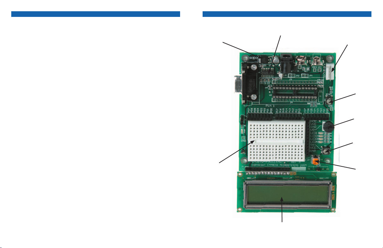
Regulator
Breadboard
RS232
Transceiver
ISSP Header
Reset
Button
POT
Button
LCD
Contrast
LCD Module
Page 4

6
7
PSOCEVAL POWER SUPPLY OPTIONS
INTRODUCTION TO MINIPROG
The following are PSoCEval power supply options:
1. Powered by the MiniProg unit.
2. Powered by a 9-12V DC wall transformer with
positive tip barrel plug and a 100 mA or higher rating.
Recommended model is CUI Inc., EPAS-101W-12.
3. Powered by a 9V battery connected to battery terminals.
4. Powered from the ICE pod in socket.
Only one of the power supplies should be used at a time. Do not
use a power supply that is less than 9V or exceeds 12V.
The Cypress MicroSystems MiniProg gives you the ability to
program PSoC parts quickly and easily.
It is small and compact, and connects to your PC using the
provided USB 2.0 cable.
During prototyping, the MiniProg can be used as an in-system
serial programmer (ISSP) to program PSoC devices on your PCB.
(See Application Notes AN2014 and AN2026 available online at
www.cypress.com for more details.)
For production purposes, it is recommended that you use the
CY3207ISSP programmer or a third-party production programmer.
Once the MiniProg is connected, you can use PSoC Programmer
software to program. (This free software can either be launched
from within PSoC Designer or run as a stand alone program.)
Page 5

8
9
SPECIFICATIONS FOR MINIPROG
OPERATING CHANGES TO THE PSOCEVAL
The operating temperature of the MiniProg is from 0° C to 50° C.
Always plug the USB cable into the MiniProg before attaching it
to the ve-pin header on the board.
When using an ISSP adapter cable with MiniProg, keep the length
under six inches to avoid signal integrity issues.
When using MiniProg, the LEDs blink at a variable rate to track
connection status. The green LED near the USB connector turns
on after MiniProg is plugged into the computer and congured by
the OS. If MiniProg cannot nd the correct driver in the system,
this LED will not turn on. After the device has been congured,
the LED stays on at about a 4-Hz blink rate. This changes during
programming, where the blink duty cycle increases.
The red LED at the bottom turns on when the MiniProg powers the
part. The LED is off when power is provided by the target board.
To use an external 32 kHz crystal oscillator, R8 and R9 on the
PSoCEval board must be removed. C9 and C10 must be added,
with values determined by the type of feedback desired. It is
recommended that you use unbalanced feedback, with C9 at 12
pF and C10 at 100 pF. (See Application Note AN2027 online at
www.cypress.com for complete details.)
To use PSoCEval at 3.3V, two parts will need to be swapped on the
board: the regulator and the RS232 transceiver, shown in Figure 1.
Suitable replacements or their equivalents are as follows:
Regulator:
TI UA78M33CKTPR
(Digikey 296-13425-1-ND)
RS232 Transceiver:
Maxim MAC3232CSE
(Digikey MAX3232CSE-ND)
Page 6

10
11
INTRODUCTION TO EXAMPLE PROJECTS
Four Example Projects are described in the following sections.
Each section is organized as follows:
EXAMPLE PROJECT #1 ADC CONVERSION
AND LCD DISPLAY
Project Name: ASM_Example_ADC_UART_LCD
Project Name: PSoC Designer project name.
Purpose: Overview of the project.
Implementation: Describes the funtionality.
Connections: Pin connections to wire up the PSoCEval board.
Pictures are included to help you verify your wiring for each
project.
Example Code (main.asm): Code to run the project.
The example projects are available in PSoC Designer. To use
them, open PSoC Designer and browse to select the correct
le. The example projects are found in …\Program Files\Cypress
MicroSystems\ PSoC Designer\Examples. Choose the chip type you
desire and open the project’s .soc le (CY8C29x66 comes with the
PSoCEval board).
When using the MiniEval programmer, do not use the “Connect”
and “Download” buttons in PSoC Designer. Theys are for use with
an In-Circuit Emulator (ICE).
Purpose: To demonstrate the 12-bit incremental ADC by
measuring the voltage of the potentiometer, transmitting the
conversion result out the UART, and displaying it on the LCD.
Implementation: This project enables the LCD, UART and
ADCINC12, and then goes into an endless loop.
In the loop, the ADC status (as it monitors the potentiometer) is
checked. If the ADC has completed a conversion, the result is
placed in “iResult” and the HEX value is transmitted out the serial
port and displayed on the LCD as ASCII text.
The clock divider VC1 provides a sample clock of 3 MHz to the
ADCINC12, resulting in a sample rate of 180 samples per second.
The clock divider VC3 generates the baud clock for the UART by
dividing 24 MHz by 156.
The UART internally divides VC3 by 8, resulting in a baud rate of
19,200 bps.
Page 7

12
13
Connections:
P01 -> VR = ADC Input (0-Vdd)
P16 -> RX = Serial RX
P27 -> TX = Serial TX
Example Code (main.asm):
// include m8c specic declarations
include “m8c.inc”
// include User Module API specic declarations
include “psocapi.inc”
export _main:
// inform assembler that variables follow
area bss(RAM)
// ADC result variable
iResult: blk 2
// inform assembler that program code follows
area text(ROM,REL)
_main:
mov A, UART_PARITY_NONE
// Enable UART
lcall UART_1_Start
mov A, >sRomString1
mov X, <sRomString1
// Display example string
lcall UART_1_CPutString
lcall UART_1_PutCRLF
mov A, PGA_1_MEDPOWER
// Turn on PGA power
lcall PGA_1_Start
mov A, ADCINC12_1_MEDPOWER
// Turn on ADC power
lcall ADCINC12_1_Start
Page 8

14
15
mov A, 0
// Sample forever
lcall ADCINC12_1_GetSamples
// Init the LCD
lcall LCD_1_Start
// row
mov A, 0
// column
mov X, 0
lcall LCD_1_Position
mov A, >sRomString2
mov X, <sRomString2
// Display string
lcall LCD_1_PrCString
// Enable Global interrupts
M8C_EnableGInt
loop:
// If conversion complete....
lcall ADCINC12_1_fIsDataAvailable
jz loop
// Get result, convert to unsigned and clear ag
lcall ADCINC12_1_iGetData
mov [iResult+1], A
mov [iResult+0], X
// add 0x0800 to result
add [iResult+0], 0x08
lcall ADCINC12_1_ClearFlag
mov A, [iResult+1]
mov X, [iResult+0]
// Print result to UART
lcall UART_1_PutSHexInt
// Tack on a CR and LF
lcall UART_1_PutCRLF
// row
mov A, 1
// column
mov X, 0
// display result in hex
lcall LCD_1_Position
mov A, [iResult+1]
mov X, [iResult+0]
lcall LCD_1_PrHexInt
jmp loop
area lit
sRomString1:
DS “Example ADC_UART_LCD”
db 00h
sRomString2:
DS “PSoC LCD”
db 00h
area text
Page 9

16
17
EXAMPLE PROJECT #2 BLINK AN LED
Project Name: ASM_Example_Blink_LED
Purpose: To demonstrate blinking an LED at a varying duty cycle
using a hardware PWM.
Implementation: The clock dividers VC1, VC2, and VC3 are used
to divide the 24 MHz system clock by 16, 16 and 256, respectively.
The resulting 366 Hz clock is used as the input to an 8-bit PWM.
This in turn produces an LED blink period of 1.4 Hz.
Connections:
P20 -> LED1
Page 10

18
19
Example Code (main.asm):
EXAMPLE PROJECT #3 OUTPUT A SINE WAVE
// include m8c specic declarations
include “m8c.inc”
// include User Module API specic declarations
include “psocapi.inc”
export _main:
_main:
// Enable PWM
lcall PWM8_1_Start
lcall PWM8_1_EnableInt
// Enable Global interrupts
M8C_EnableGInt
loop:
jmp loop
Project Name: ASM_Example_DAC_ADC
Purpose: To demonstrate a PSoC project that outputs a SINE wave
using a 6-bit DAC. The SINE wave period is based on the current
ADC value of the potentiometer.
Implementation: This project uses a 64-entry SINE look-up table
to generate values used to update a 6-bit DAC. An 8-bit counter is
utilized to generate an interrupt at the DAC update rate (1/64 SINE
wave period). By adjusting the counter period, the DAC frequency
and the resulting SINE frequency may be modied. The counter
period is reloaded with the current ADC conversion value. The
ADC input voltage may be between 0 and Vdd volts depending on
the potentiometer. At higher frequencies, SINE wave jitter may be
observed due to the large timing impact of a one-count change in
the ADC conversion.
Page 11

20
21
Connections:
P01 -> VR = ADC Input (0-Vdd)
P05 -> LED1 -> Scope = DAC Output (0-Vdd)
Example Code (main.asm):
// include m8c specic declarations
include “m8c.inc”
// include User Module API specic declarations
include “psocapi.inc”
export _main
export bADCvalue
export bTablePos
export SINtable
// inform assembler that variables follow
area bss(RAM)
// Store ADC value for debug watch variable
bADCvalue: blk 1
// Stores last table position index
bTablePos: blk 1
// inform assembler that program code follows
area text(ROM,REL)
_main:
// starts DAC value update counter
lcall Counter8_1_Start
lcall Counter8_1_EnableInt
// Turn on PGA power
mov A, PGA_1_MEDPOWER
lcall PGA_1_Start
// Turn on DAC power
mov A, DAC6_1_HIGHPOWER
Page 12

22
23
lcall DAC6_1_Start
// Turn on ADC power
mov A, DELSIG8_1_HIGHPOWER
lcall DELSIG8_1_Start
lcall DELSIG8_1_StartAD
// Enable Global interrupts
M8C_EnableGInt
loop:
// if ADC conversion complete then.....
lcall DELSIG8_1_fIsDataAvailable
jz loop
// get ADC result and convert to offset binary
lcall DELSIG8_1_cGetDataClearFlag
add A, 0x80
// store value for debug watch variable
mov [bADCvalue], A
// counter period less then 0x03 is invalid
cmp A, 0x03
// excessive interrupt servicing
jnc LoadCounter
mov A, 0x03
LoadCounter:
// update DAC update rate
lcall Counter8_1_WritePeriod
jmp loop
area lit
// 64 entry SINE look-up table
SINEtable:
db 31, 33, 36, 39, 41, 44, 46, 49, 51, 53, 55, 56, 58,
59, 59
db 60, 60, 60, 59, 59, 58, 56, 55, 53, 51, 49, 47, 44,
42, 39
db 36, 33, 31, 28, 25, 22, 19, 16, 13, 11, 9, 7, 5, 3,
2, 1, 0
db 0, 0, 0, 1, 2, 3, 4, 6, 7, 10, 12, 14, 17, 20, 23,
26, 29
area text
Page 13

24
25
EXAMPLE PROJECT #4 DYNAMICALLY
RE-CONFIGURE A PWM
The PRS conguration contains a PRS with pulse density
(analogous to pulse width) and shifted bit stream output on LEDs.
Project Name: ASM_Example_Dynamic_PWM_PRS
Purpose: To demonstrate PSoC’s dynamic re-conguration
capability by switching a digital block between a PWM8 and a
PRS8 (Pseudo Random Sequence). This example project also
demonstrates the advantages of using a PRS to generate a pulse
width. A benet of the PRS is that it does not generate the strong
frequency harmonics of an equivalent PWM.
Implementation: The clock dividers VC1, VC2, and VC3 are
used to divide the 24 MHz system clock by 16, 16, and 128,
respectively. The resulting 732 Hz clock becomes the input to an 8bit Counter User Module in the base conguration (this is the rst
conguration in PSoC Designer).
If the SW button connected on the PSoCEval board is released,
conguration PWM_cong is loaded and a period of two is loaded
into the counter.
If the button is pressed and held, conguration PRS_cong is
loaded and a period of 128 is loaded into the counter.
The PWM conguration contains a standard 8-bit PWM with
a duty cycle of 50%. Both the pulse width and terminal count
outputs are displayed on LEDs.
Connections:
P14 -> SW = User Button
P20 -> LED1 = PWM Pulse Width or PRS Pulse Density
P22 -> LED2 = PWM Terminal Count
P23 -> LED3 = PRS Bit Stream
Page 14

26
27
Example Code (main.asm):
// include m8c specic declarations
include “m8c.inc”
// include User Module API specic declarations
include “psocapi.inc”
export _main:
_main:
// congure port pins
and reg[PRT1DR], ~0x10
mov reg[PRT2DR], 0x00
// start clock generator
lcall Counter8_1_Start
// load PRS conguration
lcall LoadCong_PRS_Cong
jmp PWM
PRS:
// stop and unload PWM conguration
lcall PWM8_1_Stop
lcall UnloadCong_PWM_Cong
// then load PRS cong
lcall LoadCong_PRS_Cong
// update clock divider, don’t wait for period
reload
lcall Counter8_1_Stop
mov A, 0x7F
lcall Counter8_1_WritePeriod
lcall Counter8_1_Start
// congure and start PRS
mov A, 0x01
lcall PRS8_1_WriteSeed
mov A, 0xB8
lcall PRS8_1_WritePolynomial
lcall PRS8_1_Start
// load compare value, must be loaded after PRS is
started
mov reg[PRS8_1_SEED_REG], 0x7F
PRSloop:
// wait for button release
tst reg[PRT1DR], 0x10
jnz PRSloop
// simple debounce
tst reg[PRT1DR], 0x10
jnz PRSloop
jmp PWM
PWM:
// stop and unload PRS conguration
lcall PRS8_1_Stop
lcall UnloadCong_PRS_Cong
// then load PWM cong
lcall LoadCong_PWM_Cong
// update clock divider, don’t wait for period
reload
lcall Counter8_1_Stop
Page 15

28
29
mov A, 0x01
lcall Counter8_1_WritePeriod
lcall Counter8_1_Start
// congure and start PWM
mov A, 0xFF
lcall PWM8_1_WritePeriod
mov A, 0x7F
lcall PWM8_1_WritePulseWidth
// enable PWM
lcall PWM8_1_Start
EXAMPLE PROJECT #5 COMBINING PWMS
USING OUTPUT LOGIC
Project Name: ASM_Example_LED_Logic
Purpose: To demonstrate a PSoC project designed to blink an LED
using the output of two PWMs. The outputs are combined using an
AND gate in an output bus logic block. This logical combination
results in a beat frequency of 1.4 Hz.
PWMloop:
// wait for button release
tst reg[PRT1DR], 0x10
jz PWMloop
// simple debounce
tst reg[PRT1DR], 0x10
jz PWMloop
jmp PRS
Implementation: The clock dividers VC1 and VC2 are used to
divide the 24 MHz system clock by 16 and 16, respectively. The
resulting 93.37 kHz clock becomes the input to the two 8-bit
PWM User Modules with respective periods of 256 and 255. This
produces the LED beat frequency of 1.4 Hz.
Page 16

30
31
Connections:
P20 -> LED1
Example Code (main.asm):
// include m8c specic declarations
include “m8c.inc”
// include User Module API specic declarations
include “psocapi.inc”
export _main:
_main:
// Enable PWM1
lcall PWM8_1_Start
// Enable PWM2
lcall PWM8_2_Start
loop:
jmp loop
Page 17

CYPRESS CUSTOMER SUPPORT
We are committed to meeting your every need.
For more information about PSoC, check us out on the web at
www.cypress.com/psoc. There you will nd data sheets, hundreds
of application notes, contact information for local PSoC certied
consultants, and recorded tele-training modules for newcomers to
the PSoC world.
We offer live tele-training sessions regularly. Check online at
www.cypress.com/support/training.ctm for the next scheduled
time.
For application support please contact us online or call between 8
am – 6 pm PST at 1.800.669.0557 ext. 4814. We offer a four-hour
response time at our call center during normal business hours.
http://www.cypress.com/ http://www.cypress.com/support/
Copyright © 2004 Cypress MicroSystems, Inc. All rights reserved.
PSoC™, Programmable System-on-Chip™, and PSoC Designer™
are trademarks of Cypress MicroSystems, Inc. All other trademarks
or registered trademarks referenced herein are the property of their
respective owners. The information contained herein is subject to
change without notice. Made in the U.S.A.
32
mysupport.cfm
 Loading...