

Cypress Semiconductor PALC22V10D-25JI, PALC22V10D-25KMB, PALC22V10D-25LMB, PALC22V10D-25PC, PALC22V10D-25PI Datasheet
...
For new designs, please refer to the PALCE22V10
PALC22V10D
Flash Erasable, Reprogrammable CMOS PAL® Device
Features
• Advanced second-generation PAL architecture
•Low power
—90 mA max. commercial ( 10 ns)
—130 mA max. com me rcial (7.5 n s)
• CMOS Flash EPROM technolog y for electric al erasabil-
ity and reprogrammabilit y
• Variable product terms
—2 x(8 through 16) product terms
• User-programmable macrocell
—Output polarity control
—Individually selectable for registered or combinato-
rial operation
• Up to 22 input terms and 10 outputs
• DIP, LCC, and PLCC available
—7.5 ns commercial ver sion
5 ns t
CO
5 ns t
S
7.5 ns t
133-MHz state machine
—10 ns military and industrial ver sions
6 ns t
6 ns t
10 ns t
110-MHz state machine
—15-ns comme rc ia l an d m ilitary
versions
—25-ns comme rc ia l an d m ilitary
versions
• High reliability
—Proven Flash EPROM technology
100% programming and functional testing
PD
CO
S
PD
Functional Description
The Cypress PALC22V10D is a CMOS Flash Erasable second-generation programmable array logic device. It is implemented with the familiar sum-of-products (AND-OR) logic
structure and the programmable macrocell.
The PALC22V10D is e x e cuted in a 24- pin 300- mil mol ded DIP,
a 300-mil cerDIP, a 28-lead square ceramic leadless chip carrier , a 28-le ad square pl astic leaded chi p carrier, and provides
up to 22 in puts and 10 output s. The 2 2V10D can b e electrical ly
erased and repr ogr ammed. The prog r ammab le m acroc ell provides the capability of defining the archit ecture of each output
individually. Each of the 10 potential outputs may be specified
as “registered” or “combin atorial. ” P o larit y of each out put ma y
also be individually selected, allowing complete flexibility of
output configuration. Further configurability is provided
through “array” configurable “output enable” for each pot ential
output. This feature allows the 10 outputs to be reconfigured
as inputs on an individual basis , or alternatel y used as a combination I/O controlled by the prog rammable array.
PALC22V10D features a variable product term architecture.
There are 5 pair s of pr oduct t erm sums beg innin g at 8 pr oduc t
terms per output and incrementing by 2 to 16 product terms
per output. By providing this variable structure, the PAL C
22V10D is optimized to t he configurations found in a majority
of applications without creating devices that burden the product term structures with unusab le product terms and low er performance.
Additional features of the Cypress PALC22V10D include a
synchronous prese t and an asynchron ous r eset pro duct term.
These product terms are common to all macrocells, eliminating the need to dedicate standard product terms for initial ization function s. T he devi ce autom atically resets upo n powe r-up .
The PALC22V10D, featuring programmable macrocells and
variabl e product terms, provides a device with the flexibility to
implement logic funct ions in the 500- to 800-gate-array complexity. Since each of the 10 output pins may be individually
configured as i nputs on a tempo rary or permanent basi s, func tions requiring up to 21 inputs and only a single output and
down to 12 inputs and 10 outputs are possible. The 10 potential outputs are enabled using product terms. Any output pin
may be permanently selected as an output or arbitrarily enabled as an output and an input through the selective use of
individual product terms associated with each output. Each of
these outputs is achie v ed through an indivi dual progr ammabl e
macrocell. These macrocells are programmable to prov ide a
combinatorial or registe red in verting or non-in ve rting output. In
a registered mode of ope ration, the out put of the regist er is fed
back into t he array, providing current status information to the
array. This information is available for establishing the next result in applicat ions such as control stat e machines. In a combinatorial confi guration, the combinatorial output or, if the output is disabled, the signal present on the I/O pin is made
available to the arr ay. The flexibility provided by both program mable product t erm control of the output s and variab le produc t
terms allows a significan t gain i n functi onal densi ty throu gh the
use of programmable logic.
Along with this increase in functional density, the Cypress
PALC22V10D provides l ower-p ower oper ation t hrough the use
of CMOS technology, and increased testability with Flash reprogrammabili ty.
PAL is a registered trademark of Advanced Micro Devices
Cypress Semiconductor Corporation
• 3901 North First Street • San Jose • CA 95134 • 408-943-2600
July 1991 - Revised October 1995
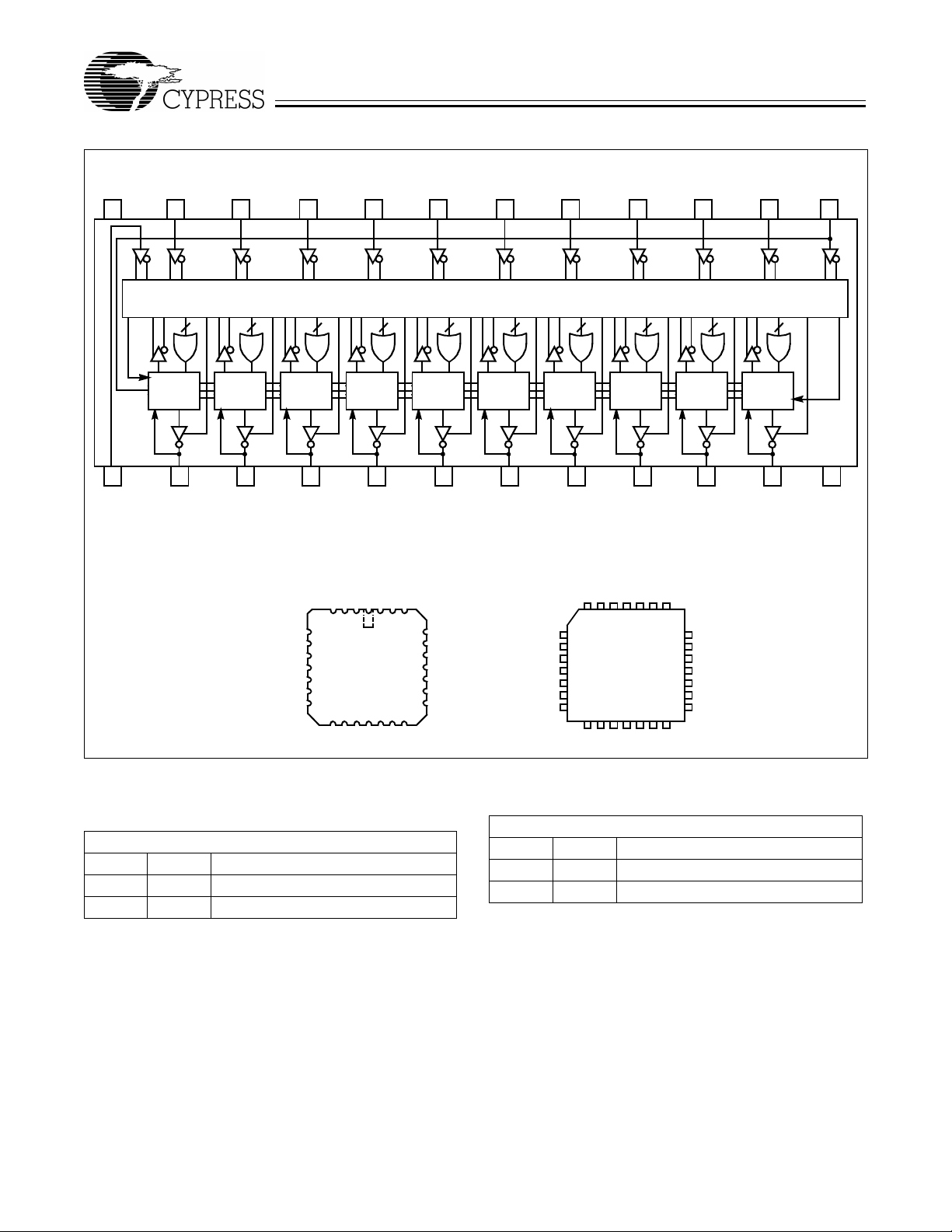
LogicBlockDiagram(PDIP/CDIP)
V
SS
IIIIIIIIIICP/I
1110987 65432112
8
Reset
10 12 14 16 16 14 12 10 8
PROGRAMMABLE
AND ARRAY
(132 X 44)
PALC22V10D
Macrocell
13 14 15 16 17 18 19 20 21 22 23 24
I I/O
Macrocell Macrocell Macrocell Macrocell Macrocell Macrocell Macrocell Macrocell Macrocell
9
I/O
8
I/O
7
I/O
6
I/O
5
I/O
4
I/O
3
I/O
2
I/O
1
I/O
0
PinConfiguration
PLCC
Top View
I9I
CP/I
4 3 2 2827 261
5
6
7
8
9
10
11
121314 1516 1718
I
I
SS
V
NC
NC
0
1
CC
V
I/O
I/O8
I/O
25
2
I/O
24
3
I/O
23
4
N/C
22
I/O
21
5
I/O
20
6
I/O
19
7
I
I/O
I/O
V10D–3
NC
I
I
I
I
I
I
LCC
Top View
I9I
CP/I
4 3 2 282726
5
6
7
8
9
10
11
12131415161718
I
I
SS
V
0
1
CC
V
I/O
I/O
NC
1
25
I/O
NC
2
24
I/O
3
23
I/O
4
22
N/C
21
I/O
5
20
I/O
6
19
I/O
7
I/O
V10D–2
8
I
I/O
NC
I
I
I
I
I
I
Configuration Table
Configuration Table
Registered/Combinatorial
C
1
0 0 Registered/Active LOW
0 1 Registered/Active HIGH
C
0
Configuration
C
1
1 0 Combinatorial/Active LOW
1 1 Combinatorial/Active HIGH
Registered/Combinatorial
C
0
Configuration
Preset
V
CC
V10D–1
2
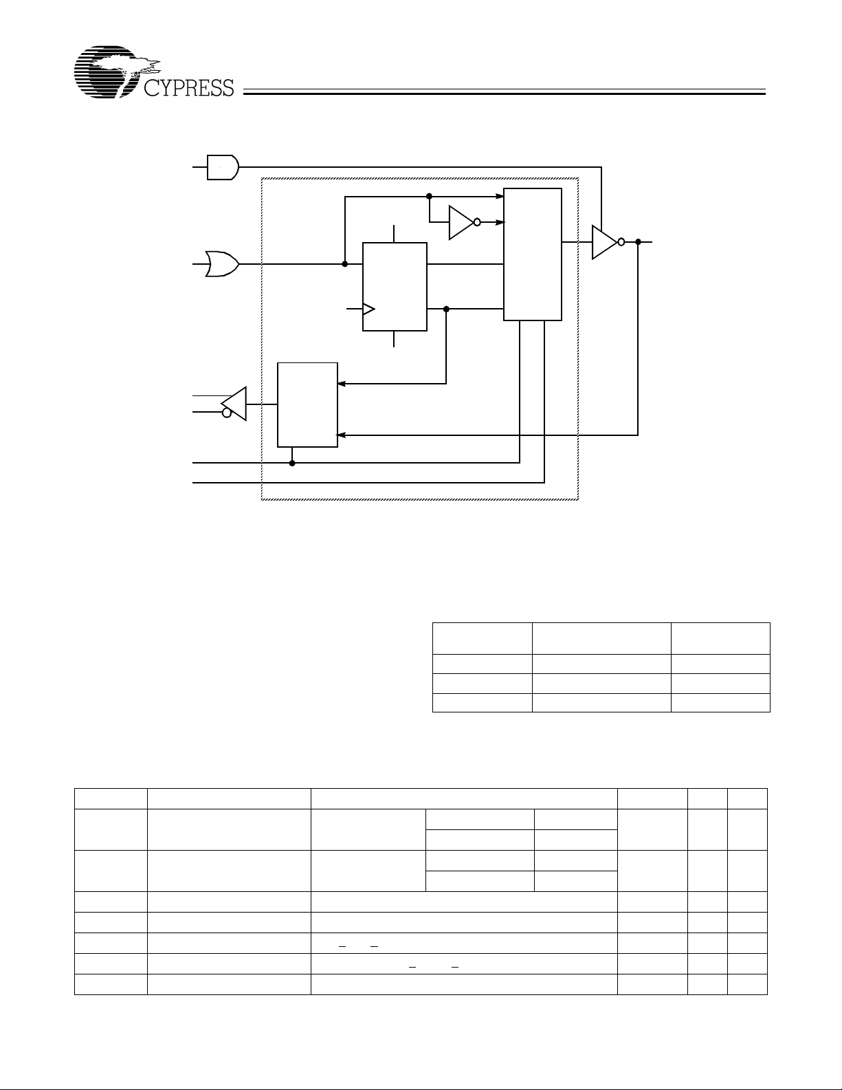
Macrocell
AR
PALC22V10D
OUTPUT
SELECT
QD
MUX
CP
INPUT/
FEEDBACK
MUX
S
1
C
1
C
0
Q
SP
MACROCELL
SS
10
V10D–4
Maximum Ratings
(Abov e which the useful lif e ma y be impai red. F or user guidelines, not tested.)
Storage Temperature .....................................−65
°
C to +150°C
Ambient Te mperature with
Power Applied..................................................−55
°
C to +125°C
Supply Voltage to Ground Potential
(Pin 24 to Pin 12).................................................−0.5V to +7.0V
DC Voltage Applied to Outp uts
in High Z State.....................................................−0.5V to +7.0V
DC Input Voltage............................................. -0.5V to +7.0V
Output C ur re n t in to O u tp u ts (LOW) ..... ................. .......16 mA
DC Programming Voltage .............................................12.5V
Electrical Characteristics
Over the Operating Range
Parameter Description T est Conditions Min. Max. Unit
V
OH
V
OL
V
IH
[2]
V
IL
I
IX
I
OZ
I
SC
Output HIGH Voltage VCC = Min.,
V
= VIH or V
IN
IL
Output LOW Voltage VCC = Min.,
V
= VIH or V
IN
IL
Input HIGH Level Guaranteed Input Logical HIGH Voltage for All Inputs
Input LOW Level Guaranteed Input Logical LOW Voltage for All Inputs
Input Leakage Current VSS < VIN < VCC, VCC = Max. -10 10
Output Leakage Current VCC = Max., VSS < V
Output Short Circuit Current VCC = Max., V
Latch-Up Current .....................................................>200 mA
Static Discharge Voltage
(per MIL-STD-883, Method 3015) .............. ............ ...>2001V
Operating Range
Ambient
Range
Commercial 0°C to +75°C 5V ±5%
[1]
Military
Industrial
Note:
1. T
is the “instant on” case temperature.
A
]]
[2]
IOH = -3.2 mA Com’l 2.4 V
IOH = -2 mA Mil/Ind
IOL = 16 mA Com’l 0.5 V
IOL = 12 mA Mil/Ind
< V
OUT
OUT
= 0.5V
CC
[5,6]
Temperature
−55°
C to +125°C 5V ±10%
−40°
C to +85°C 5V ±10%
[3]
[3]
2.0 V
-0.5 0.8 V
-40 40
-30 -90 mA
V
CC
µA
µA
3
PALC22V10D
Electrical Characteristics
Over the Operating Range
[2]
Parameter Description T est Conditions Min. Max. Unit
I
CC1
[6]
I
CC2
Notes:
2. See the last page of this specification for Group A subgroup testing information.
3. These are absolute values with respect to device ground. All overshoots due to system or tester noise are included.
4. V
IL
5. Not more than one output sho uld be t ested at a ti me. Du r ation of the short ci rcuit should not b e more tha n one sec ond. V
caused by tester g round deg r adation.
6. Tested initially and after any design or process changes that may affect these parameters.
Capacitance
Standby Power Supply
Current
VCC = Max.,
V
= GND,
IN
Outputs Open in
Unprogrammed Device
Operating Power Supply
Current
VCC = Max., VIL =
0V, V
= 3V,
IH
Output Open, Device Program m ed
as a 10-Bit Counter,
f = 25 MHz
(Min.) is equal to -3.0V for pulse durations less than 20 ns.
[6]
10, 15, 25 ns Com’l 90 mA
7.5 ns Com’l 130 mA
15, 25 ns Mil/Ind 120 mA
10 ns Mil/Ind 120 mA
10, 15, 25 ns Com’l 110 mA
7.5 ns Com’l 140 mA
15, 25 ns Mil/Ind 130 mA
10 ns Mil/Ind 130 mA
= 0.5V has been c hosen t o a void tes t prob l ems
OUT
Parameter Description T est Conditions Min. Max. Unit
C
IN
C
OUT
Endurance Characteristics
Input Capacitance VIN = 2.0V @ f = 1 MHz 10 pF
Output Capacitance V
= 2.0V @ f = 1 MHz 10 pF
OUT
[6]
Parameter Description Test Conditions Min. Max. Unit
N Minimum Reprogramming Cycles Normal Programming Conditions 100 Cycles
AC Test Loads and Waveforms
R1238
Ω
5V
OUTPUT
INCLUDING
JIG AND
SCOPE
(319ΩMIL)
C
L
R2170
Ω
(236ΩMIL)
5V
OUTPUT
INCLUDING
JIG AND
SCOPE
(a) (b)
3.0V
GND
<2ns <2ns
Equivalent to: THÉ VENIN EQUIVALENT(Commercial) Equivalent to: THÉ VENIN EQUIVALENT(Military)
99
OUTPUT
Ω
2.08V=V
thc
ALL INPUT PULSES
90%
10%
V10D–6
(319ΩMIL)
(d)
R1238
5pF
Ω
90%
OUTPUT
R2170
Ω
(236ΩMIL)
10%
V10D–5
OUTPUT
136
Ω
2.13V=V
(c)
C
L
thm
V10D–7
750
(1.2K
MIL)
Ω
Ω
4
PALC22V10D
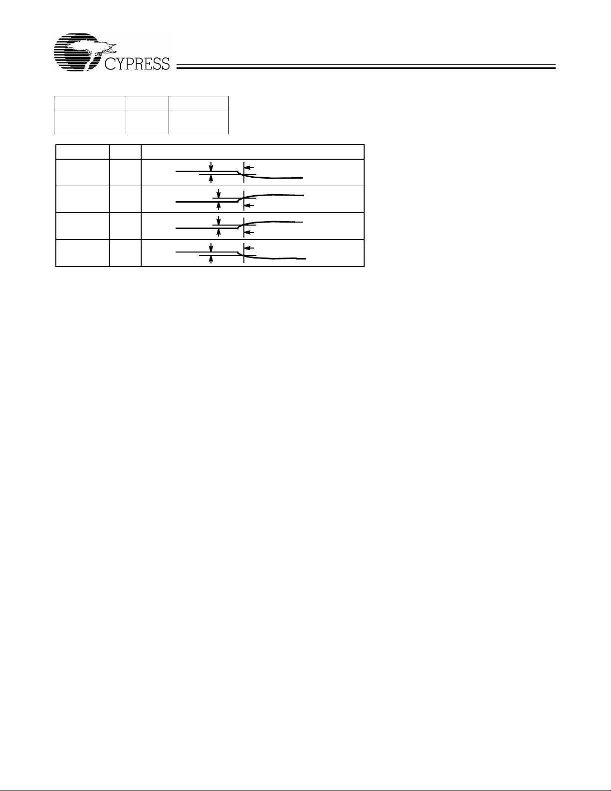
Load Speed C
L
Package
7.5, 10, 15, 25 ns50 pF PDIP, CDIP,
PLCC, LCC
Parameter V
t
ER (- )
t
ER (+)
t
EA (+)
t
EA (- )
1.5V
2.6V
0V
V
X
thc
Output Waveform Measurement Level
V
OH
0.5V
V
OL
V
V
0.5V
1.5V
X
X
0.5V
(e) Test Waveforms
V
X
V10D–8
V
X
V10D–9
V
OH
V10D–10
V
OL
V10D–11
5

PALC22V10D
Commercia l Swi tch i n g C h aracteris ti cs PALC22V10D
[2, 7]
22V10D-7 22V10D-10 22V10D-15 22V10D-25
Parameter Description Min. Max. Min. Max. Min. Max. Min. Max. Unit
t
PD
t
EA
t
ER
t
CO
t
S1
t
S2
t
H
t
P
t
WH
t
WL
f
MAX1
f
MAX2
f
MAX3
t
CF
t
AW
t
AR
t
AP
t
SPR
t
PR
Notes:
7. Part (a) of AC Test Loads and Wav eforms is used for all parameters except t
Loads and Wa veforms is used for t
8. Min. times are tested initially and after any design or process changes that may affect these parameters.
9. This specification is guaranteed for all device outputs changing state in a given access cycle.
10. The test load of part (a) of AC T est Loads and Waveforms is used for measuring t
t
EA(+)
11. This parameter is measured as the time after output disable input that the previous output data state remains stable on the output. This delay is measured to
the point at which a previous HIGH level has fallen to 0.5 volts below V
Test Loads and Waveforms for enable and di sab le tes t wa v e forms and m eas urement r ef erence l e v els .
12. This specification indicates the guaranteed maximum frequency at which a state machine configuration with external feedback can operate.
13. This specification indicates the guaranteed maximum frequency at which the device can operate in data path mode.
14. This specification indicates the guaranteed maximum frequency at which a state machine configuration with internal only feedback can operate.
15. This parameter is calculated from the clock period at f
16. The registers in the PALC22V10D have been designed with the capability to reset during system power-up. Following power-up, all registers will be reset to a
logic LOW state. The output state will depend on the polarity of the output buffer. This feature is useful in establishing state machine initialization. To insure
proper operation, the rise in V
Input to Output
Propagation Delay
[8, 9]
Input to Output Enable Delay
Input to Output Disable Delay
Clock to Output Delay
[8, 9]
[10]
[11]
37.5310315325ns
8 101525ns
8 101525ns
252728215ns
Input or Feedback Set-Up Time 5 6 10 15 ns
Synchronous Preset Set-Up Time 6 7 10 15 ns
Input Hold Time 0000ns
External Clock Period (tCO + tS)10122030 ns
[12]
[6, 13]
CF
[6, 15]
[6]
[6]
+ tS))
[6,14]
3 3 6 13 ns
3 3 6 13 ns
100 76.9 55.5 33.3 MHz
166 142 83.3 35.7 MHz
133 111 68.9 38.5 MHz
2.5 3 4.5 13 ns
Clock Width HIGH
Clock Width LOW
External Maximum Frequency
(1/(t
+ tS))
CO
Data Pa th Maximum F requency
(1/(t
+ tWL))
WH
Internal Feedback Maximum
Fr equency (1/(t
Register Clock to
Feedback Input
Asynchronous Reset Width 8 10 15 25 ns
Asynchronous Reset Recovery
5 6 10 25 ns
Time
Asynchronous Reset to
12 13 20 25 ns
Registered Outpu t Del ay
Synchronous Preset Recovery
6 8 10 15 ns
Time
Power-Up Reset Time
only . P lease see part (e) of A C Test Loads and Waveforms for ena bl e a nd disab l e test w a v ef orms and m easureme nt ref er ence le v e ls.
CC
[6,16]
.
EA(+)
must be monotonic and the t iming c onstr aints depi cted in P o w er-Up Reset W a veform must be satisfied.
1111µs
and t
. Part (b) of AC T es t Loads and Wa vefo rms is used for tER. Part (c) of A C Test
EA(+)
. The test load of part (c) of A C Test Loads and W avef orms is used f or measuring
EA(-)
internal (1/f
MAX
ER
min. or a previous LOW le ve l has risen to 0.5 volts abov e VOL max. Please see part (e) of AC
OH
) as measured (see Not e abo v e) minus tS.
MAX3
6
PALC22V10D
Military and Industrial Switching Characteristics PALC22V10D
[2, 7]
22V10D-10 22V10D-15 22V10D-25
Parameter Description Min. Max. Min. Max. Min. Max. Unit
t
PD
t
EA
t
ER
t
CO
t
S1
t
S2
t
H
t
P
t
WH
t
WL
f
MAX1
f
MAX2
f
MAX3
t
CF
t
AW
t
AR
t
AP
t
SPR
t
PR
Input to Output
Propagation Delay
[8, 9]
Input to Output Enable Delay
Input to Output Disable Delay
Clock to Output Delay
[8, 9]
[10]
[11]
310315325ns
10 15 25 ns
10 15 25 ns
2728215ns
Input or Feedback Set-Up Time 6 10 18 ns
Synchronous Preset Set-Up Time 7 10 18 ns
Input Hold Time 0 0 0 ns
External Clock Period (tCO + tS)12 20 33 ns
[12]
[6, 13]
CF
[6,15]
[6]
[6]
+ tS))
[6,14]
3614ns
3614ns
76.9 50.0 30.3 MHz
142 83.3 35.7 MHz
111 68.9 32.2 MHz
34.513ns
Clock Width HIGH
Clock Width LOW
External Maximum Frequency
(1/(t
+ tS))
CO
Data P ath Maximum F requency
(1/(t
+ tWL))
WH
Internal Feedback Maximum
Fr equency (1/(t
Regi ster Clock to
Feedba ck Input
Asynchronous Reset Width 10 15 25 ns
Asynchronous R eset
61225ns
Recovery Ti m e
Asynchronous R eset to
12 20 25 ns
Registered Output Del ay
Synchronous Preset
82025ns
Recovery Ti m e
Po wer-Up Reset Time
[6, 16]
111µs
7
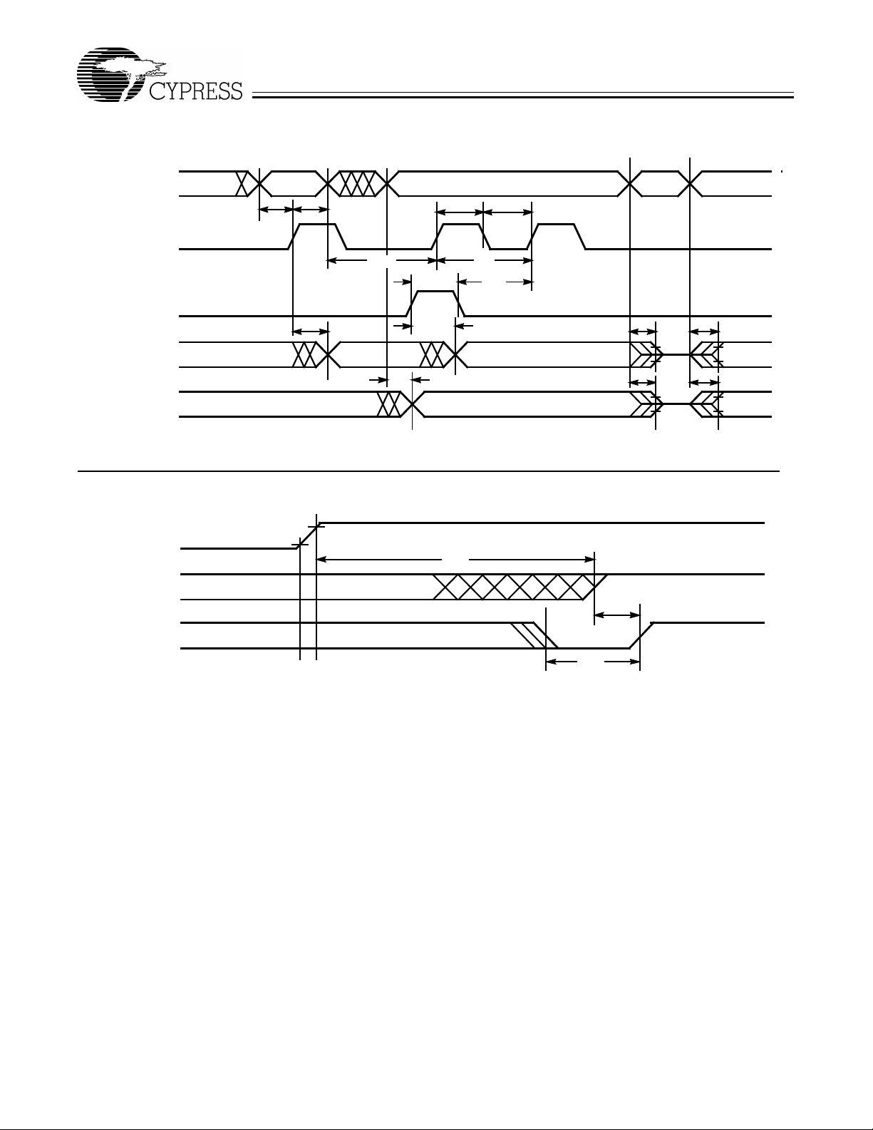
Switching Waveform
INPUTS I/O,
REGISTERED
FEEDBACK
SYNCHRONOUS
PRESET
CP
PALC22V10D
WH
t
WL
t
S
t
H
t
ASYNCHRONOUS
COMBINATORIAL
RESET
REGISTERED
OUTPUTS
OUTPUTS
Pow er-Up Reset Wa veform
SUPPLY VOLTAGE
POWER
REGISTERED
ACTIVE LOW
OUTPUTS
CLOCK
[16]
10%
t
SPR
t
AW
t
CO
t
AP
t
PD
90%
t
MAX= 1µs
PR
t
P
t
AR
[NO TAG]
t
ER
[NO TAG]
t
ER
t
PR
t
S
t
WL
[NO TAG]
t
EA
[NO TAG]
t
EA
V10D–12
V
V10D–13
CC
8

Functional Logic Diagra m for PALC22V10D
PALC22V10D
1
0
AR
OE
0
S
S
S
7
OE
0
S
S
S
OE
OE
OE
OE
9
0
S
S
S
11
0
S
S
S
13
0
S
S
S
15
0
S
S
S
2
3
4
5
4
128
16 20 24 28
32 36 40
Macro–
cell
Macro–
cell
Macro–
cell
Macro–
cell
Macro–
cell
Macro–
cell
23
22
21
20
19
18
10
11
15
6
OE
0
S
S
S
13
7
OE
0
S
S
S
11
8
OE
0
S
S
S
OE
SP
9
0
S
S
S
7
9
Macro–
cell
Macro–
cell
Macro–
cell
Macro–
cell
V10D–14
17
16
15
14
13
9

PALC22V10D
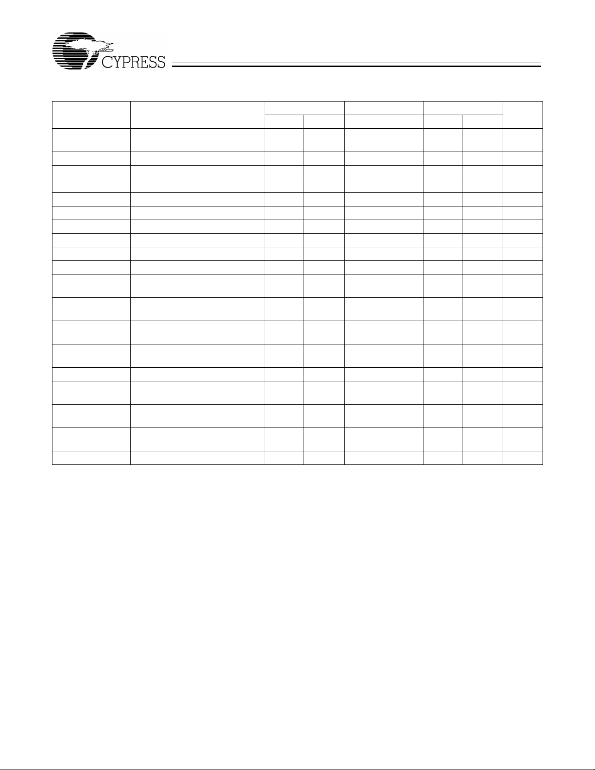
Ordering Information
I
(mA)
(ns)
t
CC
130 7.5 5 5 PALC22V10D-7JC J64 28-Lead Plastic Leaded Chip Carrier Commercial
90 10 6 7 PALC22V10D-10JC J 64 28-Lead Plastic Leaded Chi p Carrier Commercial
150 10 6 7 PALC22V10D-10JI J64 28-Lead Plastic Leaded Chip Carrier Industrial
150 10 6 7 PALC22V10D-10DMB D14 24-Lead (300-Mil) CerDIP Mil it ary
90 15 7.5 10 PALC22V10D-15JC J64 28-Lead Plastic Leaded Chip Carrier Commercial
120 15 7.5 10 PALC22V10D-15JI J64 28-Lead Plastic Leaded Chip Carrier Industrial
120 15 7.5 10 PALC22V10D-15DMB D14 24-Lead (300-Mil) CerDIP Military
90 25 15 15 PALC22V10D-25JC J64 28-Lead Plastic Leaded Chip Carrier Commercial
120 25 15 15 PALC22V10D-25JI J64 28-Lead Pl astic Leaded Chip Carrier Industrial
120 25 15 15 PALC22V10D-25DMB D14 24-Lead (300-Mil) CerDIP Military
PD
t
t
S
(ns)
CO
(ns) Ordering Code
PALC22V10D-7PC P13 24-Lead (300-Mil) Molded DIP
PALC22V10D-10PC P13 24-Lead (300-Mil) Molded DIP
PALC22V10D-10PI P13 24-Lead (300-Mil) Molded DIP
PALC22V10D-10KMB K73 24-Lead Rectangular Cerpack
PALC22V10D-10LMB L64 28-Square Leadless Chip Carrier
PALC22V10D-15PC P13 24-Lead (300-Mil) Molded DIP
PALC22V10D-15PI P13 24-Lead (300-Mil) Molded DIP
PALC22V10D-15KMB K73 24-Lead Rectangular Cerpack
PALC22V10D-15LMB L64 28-Square Leadless Chip Carrier
PALC22V10D-25PC P13 24-Lead (300-Mil) Molded DIP
PALC22V10D-25PI P13 24-Lead (300-Mil) Molded DIP
PALC22V10D-25KMB K73 24-Lead Rectangular Cerpack
PALC22V10D-25LMB L64 28-Square Leadless Chip Carrier
Package
Name Package Type
Operating
Range
MILITARY SPECIFICATIONS Group A Subgroup Testing
DC Characteristic s
Parameter Subgroups
V
OH
V
OL
V
IH
V
IL
I
IX
I
OZ
I
CC
1, 2, 3
1, 2, 3
1, 2, 3
1, 2, 3
1, 2, 3
1, 2, 3
1, 2, 3
Switchin g C h ar acteristi cs
Parameter Subgroups
t
PD
t
CO
t
S
t
H
Document #: 38-00185-H
9, 10, 11
9, 10, 11
9, 10, 11
9, 10, 11
10
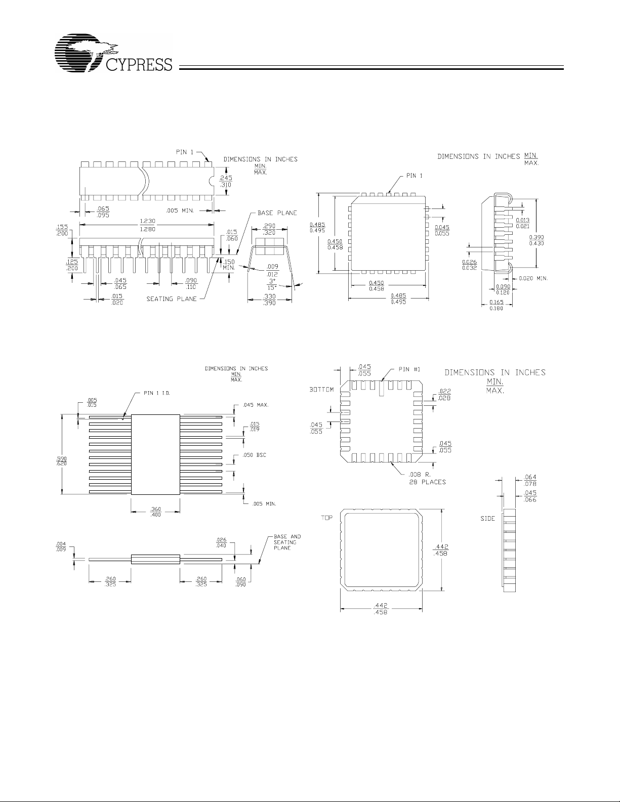
Package Diagrams
PALC22V10D
24–Lead (300–Mil) CerDIP D14
MIL-STD-1835 D-9 Config. A
24–Lead Rectangular Cerpack K73
MIL-STD-1835 F-6 Config. A
28–Lead Plastic Leaded C hip Carrier J64
28–Square Leadless Chip Carrier L64
MIL-STD-1835 C-4
11

PALC22V10D
Package Diagrams
(continue d)
24–Lead (300–Mil) Molded DIP P13/P13A
© Cypress Semiconductor Corporation, 1995. The information contained herein is subject to change without notice. Cypress Semiconductor Corporation assumes no responsibility for the use
of any circuitry other than circuitry embodied in a Cypress Semiconductor product. Nor does it conv ey or imply any lice nse under patent or other rights. Cypress Semicondu ctor does not authorize
its products for use as critical components in life-support systems where a malfunction or failure may reasonably be expected to result in significant injury to the user. The inclusion of Cypress
Semiconductor products in life-support systems application implies that the manufacturer assumes all risk of such use and in doing so indemnifies Cypress Semiconductor against all charges.
 Loading...