

Page 1

F2MC-8FX Family
MCU Board for MB95FV100D-102
MB2146-302A, Operation Manual
Doc. # 002-07488 Rev. *B
Cypress Semiconductor
198 Champion Court
San Jose, CA 95134-1709
Phone (USA): 800.858.1810
Phone (Intnl): +1.408.943.2600
www.cypress.com
Page 2

Copyrights
Copyrights
© Cypress Semiconductor Corporation, 2007-2017. This document is the property of Cypress Semiconductor Corporation
and its subsidiaries, including Spansion LLC ("Cypress"). This document, including any software or firmware included or referenced in this document ("Software"), is owned by Cypress under the intellectual property laws and treaties of the United
States and other countries worldwide. Cypress reserves all rights under such laws and treaties and does not, except as specifically stated in this paragraph, grant any license under its patents, copyrights, trademarks, or other intellectual property
rights. If the Software is not accompanied by a license agreement and you do not otherwise have a written agreement with
Cypress governing the use of the Software, then Cypress hereby grants you a personal, non-exclusive, nontransferable
license (without the right to sublicense) (1) under its copyright rights in the Software (a) for Software provided in source code
form, to modify and reproduce the Software solely for use with Cypress hardware products, only internally within your organization, and (b) to distribute the Software in binary code form externally to end users (either directly or indirectly through
resellers and distributors), solely for use on Cypress hardware product units, and (2) under those claims of Cypress's patents
that are infringed by the Software (as provided by Cypress, unmodified) to make, use, distribute, and import the Software
solely for use with Cypress hardware products. Any other use, reproduction, modification, translation, or compilation of the
Software is prohibited.
TO THE EXTENT PERMITTED BY APPLICABLE LAW, CYPRESS MAKES NO WARRANTY OF ANY KIND, EXPRESS OR
IMPLIED, WITH REGARD TO THIS DOCUMENT OR ANY SOFTWARE OR ACCOMPANYING HARDWARE, INCLUDING,
BUT NOT LIMITED TO, THE IMPLIED WARRANTIES OF MERCHANTABILITY AND FITNESS FOR A PARTICULAR PURPOSE. To the extent permitted by applicable law, Cypress reserves the right to make changes to this document without further notice. Cypress does not assume any liability arising out of the application or use of any product or circuit described in
this document. Any information provided in this document, including any sample design information or programming code, is
provided only for reference purposes. It is the responsibility of the user of this document to properly design, program, and test
the functionality and safety of any application made of this information and any resulting product. Cypress products are not
designed, intended, or authorized for use as critical components in systems designed or intended for the operation of weapons, weapons systems, nuclear installations, life-support devices or systems, other medical devices or systems (including
resuscitation equipment and surgical implants), pollution control or hazardous substances management, or other uses where
the failure of the device or system could cause personal injury, death, or property damage ("Unintended Uses"). A critical
component is any component of a device or system whose failure to perform can be reasonably expected to cause the failure
of the device or system, or to affect its safety or effectiveness. Cypress is not liable, in whole or in part, and you shall and
hereby do release Cypress from any claim, damage, or other liability arising from or related to all Unintended Uses of Cypress
products. You shall indemnify and hold Cypress harmless from and against all claims, costs, damages, and other liabilities,
including claims for personal injury or death, arising from or related to any Unintended Uses of Cypress products.
Cypress, the Cypress logo, Spansion, the Spansion logo, and combinations thereof, WICED, PSoC, CapSense, EZ-USB, FRAM, and Traveo are trademarks or registered trademarks of Cypress in the United States and other countries. For a more
complete list of Cypress trademarks, visit cypress.com. Other names and brands may be claimed as property of their respective owners.
F2MC-8FX Family, MCU BOARD for MB95FV100D-102 MB2146-302A, Operation Manual, Doc. # 002-07488 Rev. *B 2
Page 3

Preface
Thank you for purchasing the MCU board for the F2MC*-8FX family MB95FV100D-102 (model number: MB2146-302A).
The MB2146-302A is a development support tool for developing and evaluating applied products
based on the F
This manual is intended for engineers who use the MB2146-302A (referred to below as the MCU
board) to develop applied products based on Cypress F
ual describes how to handle the MCU board and its functions as well as the setting procedures.
Be sure to read this manual before using the MCU board.
Be sure to read this manual before using the MCU board.
■ Using the product safely
This manual contains important information required for using the MB2146-302A safely. Be sure to
read through the manual before using the product and follow the instructions contained therein to
use it correctly.
In particular, carefully read the “Caution of the products described in this document” at the beginning
of this manual to understand the requirements for safe use of the product before using it.
After reading the manual, keep it handy for future reference.
■ Warranty and liability disclaimers
The specifications of the product are subject to change without notice.
In no event shall Cypress be liable for any loss or damages whatsoever directly or indirectly arising
out of the use of the product.
■ Product operating environment
2
MC-8FX family of microcontrollers manufactured by Cypress.
2
MC-8FX family microcontrollers. The man-
The operating temperature for the product ranges from 5 C to 35 C and the operating relative
humidity from 20% to 80%. Avoid using the product in hot or humid environment and prevent con
densation.
The product is a printed circuit board unit without a chassis such that all of the electronic components are exposed. Therefore, neither put anything on the product nor touch or let an electrically
charged material contact a metal part of it. Once the product has been powered, try to keep those
objects away from it which can short-circuit it or easily catch fire and burn. Use the product as hori
zontal as possible and avoid operating it at a place exposed to strong vibration, dust, or explosive
gas.
Note that using the product not in the above operating environment may unexpectedly cause personal injury to the user (or another person if present near the product) or physical damage to properties around the product.
F2MC-8FX Family, MCU BOARD for MB95FV100D-102 MB2146-302A, Operation Manual, Doc. # 002-07488 Rev. *B 3
-
-
Page 4

Preface
You should also keep the packaging materials used for shipping the product. They work well as they
are when you transport the product again, for example, if it becomes out of order and needs to be
repaired.
■ Related manuals
Refer to the following manuals for additional information:
■ Hardware Manual of the MCU used
■ Data Sheet of the MCU used
■ “MB2146-09 BGM Adapter Instruction Manual”
■ Related “Header Board Instruction Manuals”
■ ““SOFTUNE Workbench Operation Manual”
■ “SOFTUNE Workbench USER’S Manual”
F2MC-8FX Family, MCU BOARD for MB95FV100D-102 MB2146-302A, Operation Manual, Doc. # 002-07488 Rev. *B 4
Page 5

■ Caution of the products described in this document
The following precautions apply to the product described in this manual.
CAUTION
Cuts, Damage
Cuts
Damage
Preface
Indicates a potentially hazardous situation which, if not avoided appropriately, may
result in minor or moderate injury and/or damage to the product or the equipment
to which the product is connected, to software resources such as data, or to other
properties.
Before moving the product, be sure to turn off all the power supplies and unplug the
les. Watch your steps when carrying the product. Do not use the product in an
cab
unstable location such as a place exposed to strong vibration or a sloping surface.
Doing so may let the product fall, resulting in an injury or fault.
The product has some sharp-pointed or edged parts inevitably exposed, such as
jumper plugs. Use meticulous care in handling the product not to get injured with
such pointed parts.
Neither put anything on or apply shock to the product. Once the product has been
po
wered, do not carry it.
Doing either may cause a fault due to overloading or shock.
Damage
Damage
Damage
Damage
Damage
Damage
Since the product contains many electronic components, keep it away from direct
sun
light, high temperature, and high humidity to prevent condensation. Do not use
or store the product where it is exposed to much dust or a strong magnetic or electric field for an extended period of time.
An adverse operating or storage environment can cause a fault.
Use the product within the ranges of
its general specifications.
Operating it outside the range of any general specification may cause a fault.
To prevent electrostatic breakdown, do not let your finger or an object touch any
metal part of the connector. Before handling the product, touch a metal object (such
as a door knob) to discharge static electricity from your body.
Before turning the power on, in particular, be sure to finish making all the required
nections. To set up and use the product, follow the instructions given in this doc-
con
ument.
Using the product incorrectly or inappropriately may cause a fault.
Before plugging or unplugging any cable for this product, be sure to turn the power
ply off. When unplugging a cable, remove it while holding the connector without
sup
pulling the cable itself. Pulling the cable itself or bending it may expose or disconnect the cable core, resulting in a fault.
Because the product has no casing, it is recommended that it be stored in the original packaging. Re-transporting the product m
ay damage it to cause a fault. Keep
the packaging materials used for shipment of the product and use them when retransporting it.
F2MC-8FX Family, MCU BOARD for MB95FV100D-102 MB2146-302A, Operation Manual, Doc. # 002-07488 Rev. *B 5
Page 6

Contents
1. Product Outline 7
1.1 Product configuration...................................................................................................8
1.2 Appearance and part name .........................................................................................9
2. Checking the Delivered Product 10
3. Connections 11
3.1 Connecting the MCU board to the header board.......................................................11
3.2 Note on connection....................................................................................................12
3.3 Disconnection ............................................................................................................12
4. How to Setup 13
4.1 How to the switch and jumper plug on a MCU board setup.......................................13
4.2 How to oscillator mounting on a MCU board .............................................................14
4.3 Handling notes...........................................................................................................14
4.4 Setting of the switch and jumper plug........................................................................15
4.5 Setting of the clock input selector switch (SW2)........................................................17
4.6 Setting of the product selector switch (SW3).............................................................18
4.7 Setting of the sub clock selector jumper plug (S1) ....................................................19
4.8 Setting of the LVD2 detection voltage selector jumper plug (S2) ..............................20
5. Product Specifications 21
5.1 General specifications ...............................................................................................21
5.2 Functional explanation...............................................................................................21
5.3 Clock settings ............................................................................................................23
5.4 Header board specifications ......................................................................................24
5.5 Connector socket specifications ................................................................................24
5.6 Pin assignment of header board I/F connector..........................................................24
Revision History 29
F2MC-8FX Family, MCU BOARD for MB95FV100D-102 MB2146-302A, Operation Manual, Doc. # 002-07488 Rev. *B 6
Page 7

1. Product Outline
BGM adapter
MCU board
Header board
The MB2146-302A is the MCU board (model number: MB2146-302A) mounting an evaluation MCU
for the F
consists of a combination of three products: the header board, MCU board, and BGM adapter
(model number: MB2146-09) as shown in Figure 1-1.
Figure 1-1. System configuration
2
MC-8FX Family of Cypress 8-bit microcontrollers. The F2MC-8FX evaluation environment,
MB2146-09
F2MC-8FX Family, MCU BOARD for MB95FV100D-102 MB2146-302A, Operation Manual, Doc. # 002-07488 Rev. *B 7
Page 8
1.1 Product configuration
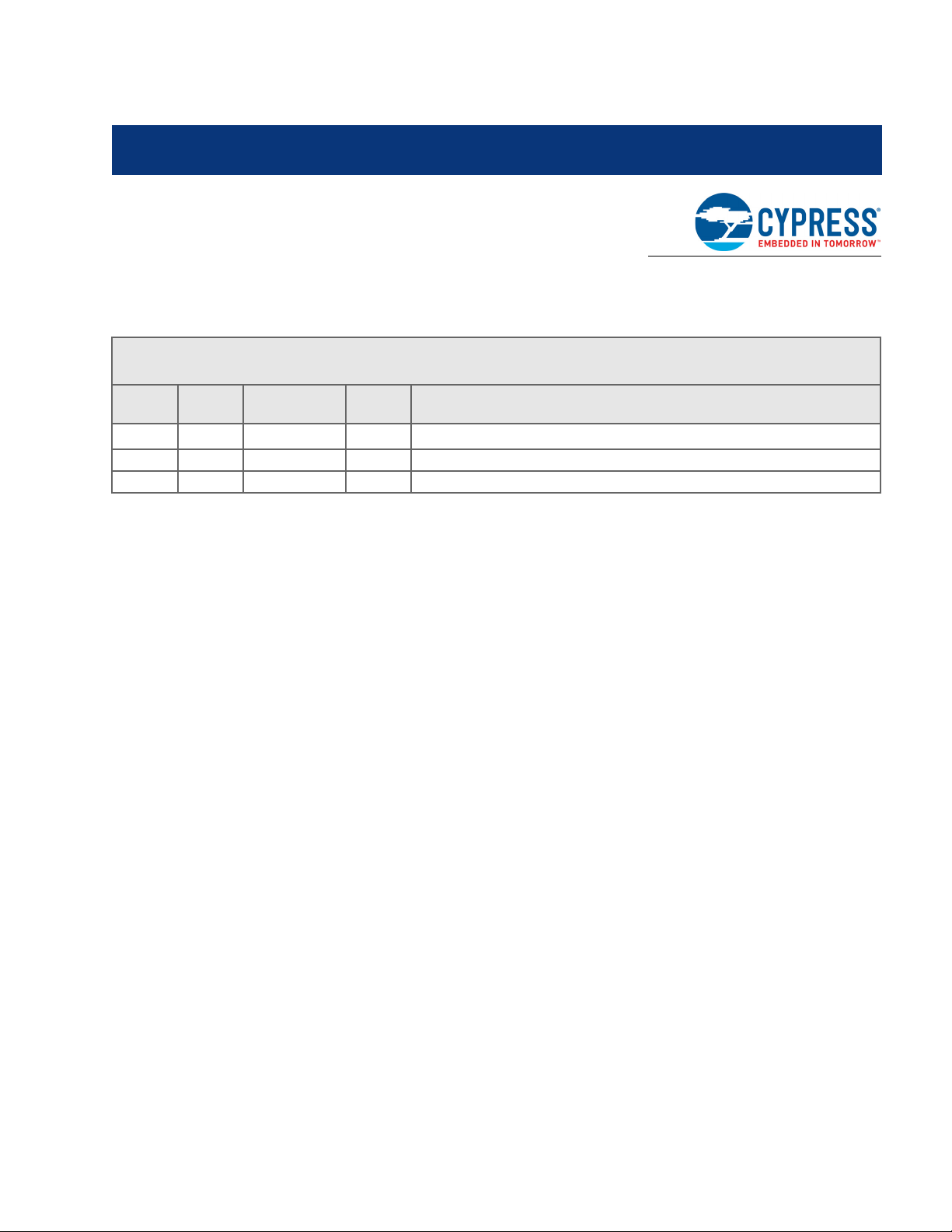
Ta bl e 1-1 lists the product configuration in the MCU board package. Table 1-2 lists optional parts for
the MCU board package that can be purchased separately.
Table 1-1. Product configuration
Name Model number Description
2
F
MC-8FX MCU board*
MB2146-302A
Product Outline
MCU board with built-in MB95FV100D10
2
* Neither the oscillator nor the capac
itor is bundled with the MB2146-302A. Therefore, prepare them
separately.
Table 1-2. Optional parts
Name Model number Description
BGM adapter*
Header board*
1
2
MB2146-09
MB2146-2xx
ICE unit for F
Connector/package conversion header
ard
bo
2
MC-8FX
*1: To use the BGM adapter, you need additional tools such as debugger software.
*2: The header board is an interface board to conn
ect the MCU board to your user system. Choose
and purchase a type of header board which is applicable to the production MCU to be used.
F2MC-8FX Family, MCU BOARD for MB95FV100D-102 MB2146-302A, Operation Manual, Doc. # 002-07488 Rev. *B 8
Page 9

1.2 Appearance and part name
* Note used during debugging.
(1) LVD2 detection voltage selector jumper plug*
(2) Voltage selector switch
(3) Product selector switch
(4) LVD selector switch
(5) Clock selector switch (SW1-1: CLK)
Clock supervisor selector switch (SW1-2 : CLK S.V.)
APB8 bus output selector switch (SW1-3: APB8) (for extension) *
C-pin selector switch (SW1-4: C)
(6) Clock input selector switch (SW2-1: X0, SW2-2: X1, SW2-3: X0A, SW2-4: X1A)
(7) Sub clock crystal oscillator mounting socket
(8) Main clock crystal oscillator mounting socket
(9) Sub clock selector jumper plug
(10) BGM adapter connector
(11) Header board I/F connector A
(12) Header board I/F connector B
(13) Evaluation MCU (MB95FV100D-102)
(14) Incorrect insertion prevention guard
Top view Bottom view
(1)
(5)
(7)
(3)
(9)
(8)
(13)
(14)
(12)
(2)
(4)
(10)
(6)
(11)
The appearance of a MCU board and the part name are shown in Figure 2.
Product Outline
Figure 1-2.
GNDVCC
LVD4
LVD3
LVD2
LVD1
LVD0
8
9
7
A
6
B
5
C
4
D
3
E
2
F
1
0
PRODUCT SELECT
ADAPTER
MCU board appearance figure
3V5V
LVD2OFFLVD1
CLK
CLK S.V.
APB8CX0X1X0A
ON ON
1 2 3 4 1 2 3 4
C B A
SUB CLOCK
BGM
X1A
1
2
MAIN CLOCK
HEADER I/F CONNECTOR A
HEADER I/F CONNECTOR B
F2MC-8FX Family, MCU BOARD for MB95FV100D-102 MB2146-302A, Operation Manual, Doc. # 002-07488 Rev. *B 9
Page 10

2. Checking the Delivered Product
Before using the MCU board, confirm that the following components are included in the box:
■ MCU board: 1
■ Operation manual (English version, this manual) : 1
■ Operation manual (Japanese version) : 1
F2MC-8FX Family, MCU BOARD for MB95FV100D-102 MB2146-302A, Operation Manual, Doc. # 002-07488 Rev. *B 10
Page 11

3. Connections
MCU board
Incorrect insertion
prevention guard
Header board
MB2146-09
MCU board
Index mark LVD2 detection voltage
selector jumper plug (S2) *
BGM adapter
BGM adapter connector (CN3)
*: Be sure to connect the BGM adapter correctly to the BGM adapter connector (CN3) on the MCU board. I
can damage the MCU board if it is accidentally connected to the LVD2 detection voltage selector jumper
plug (S2).
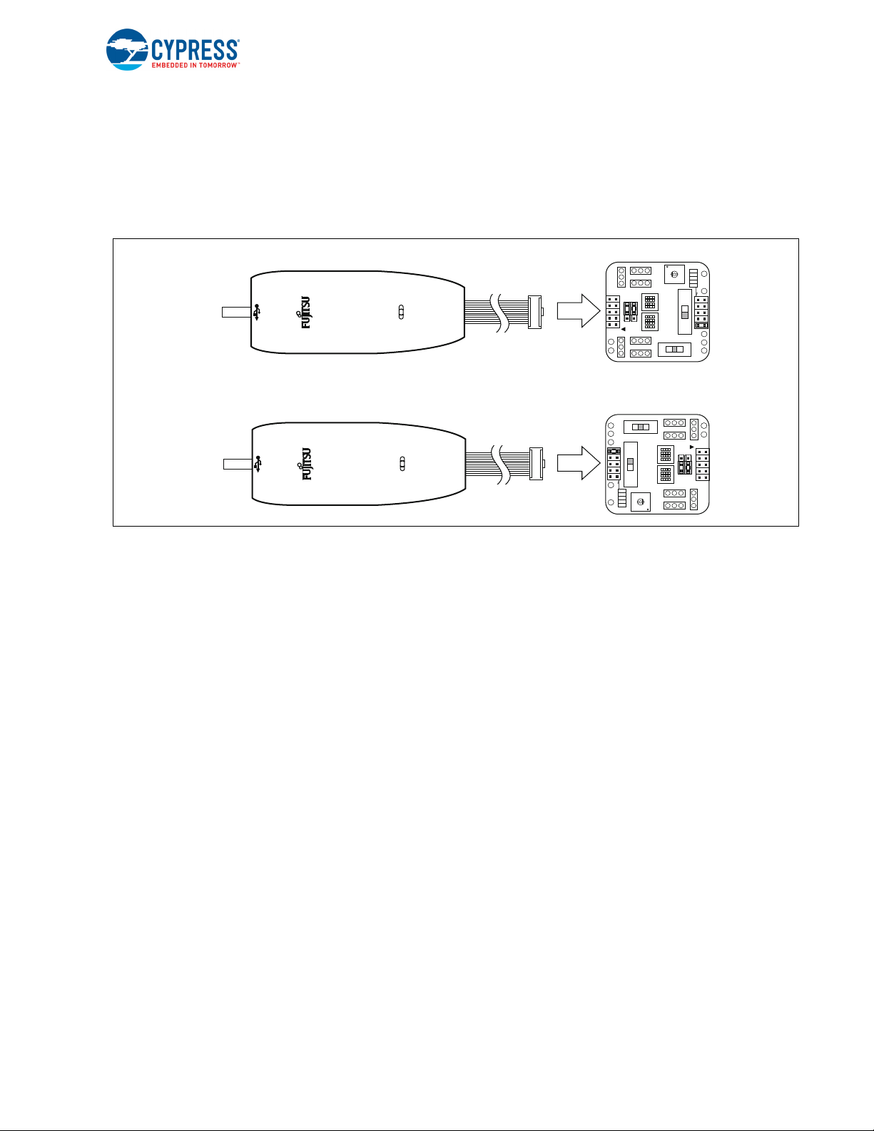
3.1 Connecting the MCU board to the header board
Align the MCU board the header board facing each other, then plug their mating connectors
together. Those connectors are provided with incorrect insertion prevention guards located diagonally. Position the two boards so that the incorrect in
each other and plug the connectors together completely (see “Figure 3-1”).
Figure 3-1.
Connection of MCU board and header board
sertion prevention guards do not interfere with
■ Connecting the MCU board to the BGM adapter
Connect the BGM adapter to the MCU board. Plu
pletely into the BGM adapter conn
ector on the MCU board such that the index marks (▼) aligned
g the BGM adapter's interface connector com-
(see “Figure 3-2”).
Figure 3-2.
Connection of MCU board and BGM adapter
ADAPTER
BGM
SUB CLOCK
C B A
2
MAIN CLOCK
PRODUCT SELECT
4
5
3
6
2
7
LVD4
1
8
0
9
LVD3
F
E
ON ON
1 2 3 4 1 2 3 4
CLK
CLK S.V.
APB8
C
X0
X1
1
X0A
X1A
GND
A
B
LVD2
D
C
VCC
LVD1
LVD0
3V5V
LVD2OFFLVD1
F2MC-8FX Family, MCU BOARD for MB95FV100D-102 MB2146-302A, Operation Manual, Doc. # 002-07488 Rev. *B 11
Page 12
3.2 Note on connection
1. Be sure to connect the BGM adapter connector (CN3). The BGM adapter connector and the
LVD2 detection voltage selector jumper plug have the same shape (see “Figure 3-3”). The MCU
board may break if the BGM adapter co
voltage selector jumper plug (S2) on the other side of the board.
Connections
nnector is accidentally plugged into the LVD2 detection
Figure 3-3.
Connection direction of BGM adapter
2. To supply a main clock signal and sub clock signa
circuit on the user system so that it supplies the clock signal to the MCU board via a buffer
circuit.
3.3 Disconnection
MB2146-09
MB2146-09
PRODUCT SELECT
4
5
3
6
7
2
LVD4
1
8
0
9
LVD3
F
GNDVCC
A
B
E
LVD2
D
OK
NG
ADAPTER
BGM
GNDVCC
SUB CLOCK
C B A
2
MAIN CLOCK
LVD2OFFLVD1
3V5V
LVD0
LVD1
LVD2
LVD3
LVD4
C
LVD1
LVD0
5V
ON ON
1 2 3 4 1 2 3 4
CLK
CLK S.V.
APB8
C
X0
X1
1
X0A
X1A
3V
LVD2OFFLVD1
1 2 3 4 1 2 3 4
ON ON
PRODUCT SELECT
MAIN CLOCK
1
2
C B A
SUB CLOCK
BGM
ADAPTER
X1A
X0A
X1
X0
C
APB8
CLK S.V.
CLK
C
D
B
E
A
F
9
0
8
1
7
2
6
3
5
4
l from the user system, provide an oscillation
a. Remove the BGM adapter from the MCU board. Holding the MCU board firmly, pull the BGM
adapter vertically from the BGM adapter connector on the MCU board.
b. Remove the header board from the MCU board. Remove it with uniform force without applying
force to only one point.
F2MC-8FX Family, MCU BOARD for MB95FV100D-102 MB2146-302A, Operation Manual, Doc. # 002-07488 Rev. *B 12
Page 13

4. How to Setup
4.1 How to the switch and jumper plug on a MCU board setup
Please set the following switches referring to “Figure 6 The switch and jumper plug on a MCU
board”.
1. Set the clock selector switch (SW1-1) to ON or
tively.
2. Set the clock supervisor select
or switch (SW1-2) to OFF.
3. Set the C-pin selector switch (SW1-4) to OFF.
4. Set the clock input selector switch (SW2).
Check that value with “Setting of the clock input
5. Set the product selector switch (SW3) to the valu
production MCU.
Check that value with “Setting of the product select
6. Set the LVD selector switch (SW4) to OFF.
7. Set the power supply selector switch (SW5) to 3V.
8. Set the sub clock selector jumper plug (S1).
OFF to disable or enable the sub clock, respec-
selector switch (SW2)”.
e corresponding to the number of pins on the
or switch (SW3)”.
Check that value with “Setting of the sub clock selector jumper plug (S1)”.
Please use with following settings, because
■ Set the APB8 bus output selector switch (SW1-3) to OFF.
■ Set the LVD2 detection voltage selector jumper plug (S2) to LVD0.
APB8 bus and LVD2 functions are not available.
Check that value with “Setting of the LVD2 detection voltage selector jumper plug (S2)”.
Figure 4-1.
The switch and jumper plug on a MCU board
S2
GND VCC
LVD4
LVD3
LVD2
8
9
7
A
6
B
5
C
4
D
3
E
2
F
1
0
PRODUCT SELECT
SC5 SC6
SC4
ADAPTER
5V
LVD1
LVD0
SW5
SW3
CLK
CLK S.V.
APB8CX0X1X0A
ON ON
1 2 3 4 1 2 3 4
SW1 SW2
S1
C B A
SUB CLOCK
BGM
3V
X1A
1
2
MAIN CLOCK
LVD2OFFLVD1
SW4
SC3 SC2
SC1
F2MC-8FX Family, MCU BOARD for MB95FV100D-102 MB2146-302A, Operation Manual, Doc. # 002-07488 Rev. *B 13
Page 14

4.2 How to oscillator mounting on a MCU board
Ceramic oscillator
Crystal oscillator
Capacitor mounting socket
Crystal oscillator
mounting socket
GND
Capacitor mounting socket
■ For information on the crystal oscillator such as its frequency, refer to the data-
sheet for the evaluation MCU.
■ For the capacitance of the capacitor, refer to the datasheet for the crystal oscilla-
tor, etc.
■ Neither the crystal oscillator nor the capacitor is bundled with this product.
Mount a crystal or ceramic oscillator in the crystal oscillator mounting sockets (for the main clock and
sub clock) on the MCU board.
How to Setup
The MCU board has one crystal oscillator mounting socket
for the main clock and the other for the
sub clock. To distinguish them from each other, the board has the “MAIN CLOCK” and “SUB
CLOCK” labels are printed on the board near the main clock socket and sub clock socket. Mount the
crystal or ceramic oscillator along with the capacitors on the MCU board (see “Figure 4-2”).
Figure 4-2.
The example of mount of crystal or ceramic oscillator
4.3 Handling notes
1. Data can not be written/erased to lower banks (1000H to 3FFFH) in the software development
2
support environment for the F
2. Do not perform a chip erase when using the so
2
MC-8FX (MB95FV100D and MB2146-09).
F
F2MC-8FX Family, MCU BOARD for MB95FV100D-102 MB2146-302A, Operation Manual, Doc. # 002-07488 Rev. *B 14
MC-8FX (MB95FV100D and MB2146-09).
ftware development support environment for the
Page 15

4.4 Setting of the switch and jumper plug
BGM
ADAPTER
SUB CLOCK
C B A
1
2
CLK
CLK S.V.
APB8CX0X1X0A
X1A
7
6
5
4
3
2
1
0
F
E
D
C
B
A
9
8
PRODUCT SELECT
LVD4
LVD3
LVD2
LVD1
LVD0
GNDVCC
3V5V
LVD2OFFLVD1
MAIN CLOCK
1 2 3 4 1 2 3 4
ON
ON
SW5
SW3
SW1 SW2
S1
SC5 SC6
SC4
SC3 SC2
SC1
S2
LVD4
LVD3
LVD2
LVD1
LVD0
SW4
The positions of the switch and jumper plug on the MCU board is shown in Figure 4-3, and specifications are shown in Ta bl e 4-1.
How to Setup
Figure 4-3.
Positions of switches and jumper plugs on the MCU board
Table 4-1. Switch and jumper plug settings
Switch/Jumper plug Settings
Clock selector switch SW1-1
Clock supervisor selector
SW1-2
switch
APB8 bus output se-
lector
SW1-3
switch
ON : Disable the sub clock
OFF : Enable the sub clock
ON : Enable the clock supervisor function
OFF : Disable the clock supe
ON : Enable the APB8 bus
OFF : Disable the APB8 bus
rvisor function
Shipment
setting
OFF
OFF
OFF
ON : Connect the C pin to the on-board
C-pin selector switch SW1-4
Clock input selector
switch
SW2
0.
OFF : Disconnect the C pin from the on-board
1F capacitor
0.
Select the main clock and
sub clock source
on the MCU board or on the user system
(See “Setting of the clock input selector
OFF
OFF
1F capacitor
switch (SW2)”).
Product selector
switch
F2MC-8FX Family, MCU BOARD for MB95FV100D-102 MB2146-302A, Operation Manual, Doc. # 002-07488 Rev. *B 15
SW3
Set this switch depending on the number of
s on the target MCU to be used (See “Set-
pin
ting of the product selector swit
ch (SW3)”).
0
Page 16

How to Setup
Switch/Jumper plug Settings
Select the low-voltage detection function.
LVD selector switch SW4
LVD1 : LVD1 enabled
OFF : LVD function disabled
LVD2 : LVD2 enabled
Select 5V or 3V supply for the operating volt-
Voltage selector switch SW5
age of the evaluation MCU.
5V : 5V supply
3V : 3V supply
Sub clock selector
jumper plug
LVD2 detection voltage selector jumper
plug
S1
S2
Select whether to use the sub clock.
(See Setting of the sub clock selector jumper
plug (S1)”).
Set the LVD2 detection voltage (See “Setting
of the LVD2 detection voltage selector jumper
plug (S2)”).
Shipment
setting
OFF
3V
Jumper of
B-C
LVD0
F2MC-8FX Family, MCU BOARD for MB95FV100D-102 MB2146-302A, Operation Manual, Doc. # 002-07488 Rev. *B 16
Page 17

4.5 Setting of the clock input selector switch (SW2)
Figure 4-4 shows the clock input selector switch. Ta bl e 4-2 lists switch positions for the main clock
supply source. Table 4-3 lists switch positions for the sub clock supply source.
How to Setup
Figure 4-4.
Clock input selector switch (SW2)
X0
X1
X0A
ON
1 2 3 4
Table 4-2. Setting of main clock supply source
Main clock supply source
Clock area OFF OFF
User system ON ON
Table 4-3. Setting of the sub clock supply source
Sub clock supply source
Clock area OFF OFF
User system ON ON
Settings of the clock input selector switch
Settings of the clock input selector switch
X1A
SW2-1 SW2-2
SW2-3 SW2-4
F2MC-8FX Family, MCU BOARD for MB95FV100D-102 MB2146-302A, Operation Manual, Doc. # 002-07488 Rev. *B 17
Page 18

4.6 Setting of the product selector switch (SW3)
Ta bl e 4-4 lists the setting of product selector switch and product type.
Table 4-4. Setting of the product selector switch
Switch setting Product type
0 100-pin package type
1 80-pin package type
2 64-pin package type
3 48-pin, 52-pin package type
4 32-pin package type
5 28-pin package type
6 20-pin package type
7 Setting Prohibited
8 100-pin package, LCD function integrated type
9 80-pin package, LCD function integrated type
A 64-pin package, LCD function integrated type
B 48-pin, 52-pin package, LCD function integrated type
C
D
E
F
Setting Prohibited
How to Setup
F2MC-8FX Family, MCU BOARD for MB95FV100D-102 MB2146-302A, Operation Manual, Doc. # 002-07488 Rev. *B 18
Page 19

4.7 Setting of the sub clock selector jumper plug (S1)
C B A
1
2
C B A
1
2
Example 1 Example 2
Ta bl e 4-5 lists jumper plug positions and sub clock selection. Figure 4-5 shows examples of sub
clock selection.
Table 4-5. Setting of sub clock selector
Settings of the sub
- 1: C
A - 1: B
clock
(S1)
Jumper of
2: B - 2: C
Jumper of
2: A - 2: B
Sub clock
Used Supply source M1 correspondence pin X0A X1A
enable
disable
Clock area
User system*
X0A : R3 pin
X1A : V1 pin
selector jumper plug
Jumper of
1: B
Jumper of
1:
How to Setup
Example of
settings
Example 1
Example 2
* Oscillation is not guaranteed when the c
Figure 4-5.
The example of sub clock selection
rystal oscillator is mounted on the user system.
F2MC-8FX Family, MCU BOARD for MB95FV100D-102 MB2146-302A, Operation Manual, Doc. # 002-07488 Rev. *B 19
Page 20

How to Setup
LVD4
LVD3
LVD2
LVD1
LVD0
4.8 Setting of the LVD2 detection voltage selector jumper plug (S2)
Figure 4-6 shows the setting of the LVD2 detection voltage selector jumper plug (S2). Table 8 lists
jumper plug positions for detection voltages.
These settings cannot be used during debugging. Se
Figure 4-6.
Table 4-6. Setting of the LVD2 detection
The LVD2 detection voltage selector jumper plug (S2)
voltage selector jumper plug
Jumper plug position LVD2 setting value
LVD0 Å{4.17V
LVD1 Å{3.74V
LVD2 Å{3.3V
LVD3 Å{2.9V
LVD4 Å{2.6V
t the jumper to LVD0 to use the debugger.
F2MC-8FX Family, MCU BOARD for MB95FV100D-102 MB2146-302A, Operation Manual, Doc. # 002-07488 Rev. *B 20
Page 21

5. Product Specifications
5.1 General specifications
The general specifications of the MCU board are shown in Tab le 5-1.
Table 5-1. MCU board general specifications
Item Specification
Name
Model number MB2146-302A
Power supply
Frequency of
ration
ope
Operating tem-
perature
Operating humid-
ity
Dimensions 40.0mm (W) 40.0mm (
Weight 13g
MCU board for the F
E
valuation MCU (MB95FV100D-102) : Å{3.3V (UVcc)
MCU board power supply : Å{3.3V (supplied by the user system)
Max. 16.25MHz
5 C to 35 C
20Åì to 80Åì(No condensation is allowed.)
2
MC-8FX MB95FV100D-102
D) 14.6mm (H)
5.2 Functional explanation
The functional specifications of the MCU board are shown inTable 5-2, and a functional block dia-
gram is shown in Figure 5-1.
Table 5-2. MCU board functional specifications
Item Description
MCU board function
Switches
Jumper plugs
Clock mounting
socket
F2MC-8FX Family, MCU BOARD for MB95FV100D-102 MB2146-302A, Operation Manual, Doc. # 002-07488 Rev. *B 21
Serves as the adapter used in combination with the BGM adapter and header board to
e connection between the BGM adapter and
provid
evaluation MCU and between the evaluation MCU and user system.
Serve for clock selection, clock supervisor selection,
selection, C-pin setting, c
and voltage selection.
The jumper plugs on the MCU board can be used to make various
settings for low-voltage detection and clock selection.
The crystal oscillator mounted socket on the MCU b
to the main clock (X0/X1) and sub clock (X0A/X1A) pins on the evaluation MCU from the
MCU board.
lock selection, product selection, low-voltage detection setting,
APB8 bus output
oard is used to supply clock signals
Page 22

Figure 5-1. MCU board functional block diagram
AVcc
AVR
AVss
AVcc3
AVR3
Vcc
C
PG0
SEL4
SEL0
SEL1
SEL2
SEL3
LVR0
LVR1
LVR2
LVR3
LVR4
LVDIN
X0,X1,
X0A,X1A
LVDEN2
LVDEN
LVDREXT
APBEN
CSVEN
Vcc,GND,BRSTX,
BSIN,BSOUT,
BDBMX,BEXCK
0
0
0
0
0
0
0
0
1
2
1
1
1
1
1
1
1
1
4
2
3
1
2
3
4
5
0
1
Header board
I/F
connector
Header board
I/F
connector
Voltage
selector
switch
C-pin
selector
switch
Product
selector
switch
Clock selector
switch
MB95FV100D-102
(Evaluation MCU)
Other pins
LVD2 detection voltage
setting jumper plug
BGM
adapter
connector
Clock
selector
circuit
LVD
selector
switch
APB8 bus output
selector switch
Clock supervisor
selector switch
Product Specifications
F2MC-8FX Family, MCU BOARD for MB95FV100D-102 MB2146-302A, Operation Manual, Doc. # 002-07488 Rev. *B 22
Page 23

5.3 Clock settings
Clock input
selector switch
Crystal oscillator mounting
socket (main clock)
Sub clock selector
jumper plug
Crystal oscillator
mounting socket
(sub clock)
Figure 5-2 shows the clock-related circuit diagram.
Figure 5-2. Clock selector circuit
Product Specifications
(M1)
X0A
X1A
(R1)
X0
T4
X1
U2
R3
V1
GND
GND
CBA
1
2
3
4
1
2
X0
X1
X0A
X1A
F2MC-8FX Family, MCU BOARD for MB95FV100D-102 MB2146-302A, Operation Manual, Doc. # 002-07488 Rev. *B 23
Page 24

5.4 Header board specifications
MCU board I/F
connector B
MCU board I/F connector A
30mm
40mm
20mm
40mm
18mm
20mm
13mm
Incorrect insertion
prevention guard
Figure 5-3 shows recommended dimensions of the header board connected to the MCU board.
Ta bl e 5-3 lists the general specifica
Figure 5-3. Recommended dimensions of the header board (Top view)
tions of the header board.
Product Specifications
1212
119120119120
Table 5-3. General specifications of the header board.
Item Description
120 pin 0.5mm pitch 2 piece connector (Straight) 2
MCU board interface connector
Incorrect insertion prevention guard
Spacing between the MCU and header boards when
aged
eng
Model
number: WR-120SB-VF-N1(Japan Aviation
Electronics Industry, Limited)
2 pin SIP socket
Model number: PCW-3-1-1PW (MAC EIGHT)
Approx. 5.0mm
5.5 Connector socket specifications
The specifications of a connector and a socket is shown in Tab le 5-4
Table 5-4. Connector and socket specifications
Item Description
Header board interface connector Connects the MCU board to the header board.
BGM adapter connector Connects the MCU board to the BGM adapter.
Main clock mounting socket Mounts the main clock crystal oscillator.
Sub clock mounting socket Mounts the sub clock crystal oscillator.
5.6 Pin assignment of header board I/F connector
F2MC-8FX Family, MCU BOARD for MB95FV100D-102 MB2146-302A, Operation Manual, Doc. # 002-07488 Rev. *B 24
Ta bl e 5-5 and Table 5-6 lists the pin assignments of the header board interface connectors on the
MCU board
Page 25

Table 5-5. Pin assignment of header board I/F connector A
Product Specifications
Connector
Pin
Number
1
2 B9 PC1 42 E1 LVSS * 82 P4 BDBMX
3 C9 PC2 43 F4
4 D9 PC3 44 F3
5 A8 PC0 45 F2
6 B8 PB4 46 F1 P22A 86 R4 RSTX
7 C8 PB5 47 GND * 87 T1 ROMS1
8 D8 PB6 48 GND * 88 T2 BSIN
9 A7 PB7 49 G4 P20A 89 T3 Vss *
10 B7 PB2 50 G3 NC1 90 T4 X0
11 C7 PB0 51 G2 P21A 91 U1 BEXCK
12 D7 PB1 52 G1 P23A 92 U2 X1
13 A6 PB3 53 H4 P24A 93 U3 MOD
14 B6 PA 2 54 H3 P25A 94 U4 PF2
15 C6 P95 55 H2 P26A 95 V1 X1A
16 D6 PA0 56 H1 P27A 96 V2 Vcc53 *
17 A5 PA 3 57 J4 P24B 97 GND *
18 B5 P94 58 J3 P50 98 GND *
19 C5 P90 59 J2 P23B 99 V3 PINT0
20 D5 P91 60 J1 P51 100 V4
21 A4 PA 1 61 K1 P52 101 R5 PF1
22 A3 P93 62 K2 P55 102 T5 PF0
23 GND * 63 K3 P54 103 U5 NC2
24 GND * 64 K4 P53 104 V5
25 A2 CSVENX 65 L1 P70 105 R6 APBENX
26 A1 Vss * 66 L2 P74 106 T6 PINT1
27 B4 P92 67 L3 P73 107 U6 PCLK
28 B3 TCLK 68 L4 P72 108 V6 PADDR0
29 B2 LVCC * 69 M1 P71 109 R7
30 B1 LV DIN 70 M2 P76 11 0 T7 PLOCK
31 C4 Cpin 71 M3 P80 111 U7 PWRITE
32 C3 Vcc51 * 72 M4 P77 112 V7 PADDR1
33 C2 LVDENX2 73 GND * 113 R8 PADDR2
34 C1 LVR4 74 GND * 114 T8 PADDR3
35 D4 TESTO 75 N1 P75 11 5 U8 PADDR4
36 D3 LVD OUT 76 N2 P82 116 V8 PADDR5
Evaluation
MCU Pin
Number
A9 PC4 41 E2 LV R3 81 P3 BSOUT
Signal
line
name
Connector
Pin
Number
Evaluation
MCU Pin
Number
Signal
line
name
LVDRE
XT
LVD BGR
LVD EN
X
Connector
Pin
Number
83 R1 P83
84 R2 BRSTX
85 R3 X0A
Evaluation
MCU Pin
Number
Signal
line
name
PSEL_E
XT
PENABLE
PAC -
TIVE
F2MC-8FX Family, MCU BOARD for MB95FV100D-102 MB2146-302A, Operation Manual, Doc. # 002-07488 Rev. *B 25
Page 26

Product Specifications
Connector
Pin
Number
37 D2 LVR2 77 N3 PG0 11 7 R9 PADDR7
38 D1 BGOENX 78 N4 P84 118 T9
39 E4 LV R1 79 P1 P81 119 U9 PADDR6
40 E3 LV R0 80 P2 ROMS0 120 V9
Evaluation
MCU Pin
Number
Signal
line
name
Connector
Pin
Number
Evaluation
MCU Pin
Number
Signal
line
name
Connector
Pin
Number
Evaluation
MCU Pin
Number
Signal
line
name
PRDA-
TA0
PRDA-
TA1
F2MC-8FX Family, MCU BOARD for MB95FV100D-102 MB2146-302A, Operation Manual, Doc. # 002-07488 Rev. *B 26
Page 27

Table 5-6. Pin assignment of header board I/F connector B
Product Specifications
Connector
Pin
Number
1 A10 PC5 41 E17 NC4 81 P16 P34
2 B10 PD0 42 E18 SEL0 82 P15 P35
3 C10 PC6 43 F15 SEL3 83 R18 P44
4 D10 PC7 44 F16 SEL4 84 R17 P36
5 A11 PD1 45 F17 SEL1 85 R16 P31
6 B11 PD2 46 F18 P04C 86 R15 AV cc3
7 C11 PD3 47 GND * 87 T18 P40
8 D11 PD4 48 GND * 88 T17 P32
9 A12 PD5 49 G15 P06C 89 T16 AVs s
10 B12 PD7 50 G16 P07C 90 T15 AV R
11 C12 P61 51 G17 P05C 91 U18 P33
12 D12 P60 52 G18 P00C 92 U17 P30
13 A13 PD6 53 H15 P01C 93 U16 AV R3
14 B13 P64 54 H16 P02C 94 U15 P15
15 C13 P66 55 H17 P03C 95 V18 AVcc
16 D13 P65 56 H18 P07A 96 V17 DA0
17 A14 P62 57 J15 P04A 97 GND *
18 B14 PE0A 58 J16 P05A 98 GND *
19 C14 PE3A 59 J17 P06A 99 V16 P14
20 D14 PE2A 60 J18 P03A 100 V15 P10
21 A15 P63 61 K18 P02A 101 R14 P16
22 A16 P67 62 K17 P07B 102 T14 DA1
23 GND * 63 K16 P01A 103 U14 P13
24 GND * 64 K15 P00A 104 V14
25 A17 PE4A 65 L18 P06B 105 R13 P11
26 A18 Vcc54 * 66 L17 P05B 106 T13 P12
27 B15 PE1A 67 L16 P04B 107 U13 NC3
28 B16 PE5A 68 L15 P03B 108 V13
29 B17 PE7A 69 M18 P02B 109 R12
30 B18 PE3B 70 M17 P00B 110 T12
31 C15 PE6A 71 M16 P46 111 U12
32 C16 Vss * 72 M15 P47 11 2 V12
33 C17 PE2B 73 GND * 113 R11
34 C18 PE7B 74 GND * 114 T11
35 D15 PE1B 75 N18 P01B 11 5 U11
Evaluation
MCU Pin
Number
Signal
line
name
Connector
Pin
Number
Evaluation
MCU Pin
Number
Signal
line
name
Connector
Pin
Number
Evaluation
MCU Pin
Number
Signal
line
name
PWDA-
TA7
PWDA-
TA3
PWDA-
TA5
PWDA-
TA6
PWDA-
TA4
PRDA-
TA7
PWDA-
TA0
PWDA-
TA1
PWDA-
TA2
F2MC-8FX Family, MCU BOARD for MB95FV100D-102 MB2146-302A, Operation Manual, Doc. # 002-07488 Rev. *B 27
Page 28

Product Specifications
Connector
Pin
Number
36 D16 PE0B 76 N17 P43 116 V11
37 D17 PE6B 77 N16 P41 117 R10
38 D18 SEL2 78 N15 P42 118 T10
39 E15 PE5B 79 P18 P45 119 U10
40 E16 PE4B 80 P17 P37 120 V10
Evaluation
MCU Pin
Number
Signal
line
name
Connector
Pin
Number
Evaluation
MCU Pin
Number
Signal
line
name
Connector
Pin
Number
*: About power supply pins (common to connectors A and B)
Connect the Vcc51, Vcc53 and Vcc54 pins to
Connect the Vss pin to GND. Disco
nnect the LVSS pin from GND.
Vcc. Disconnect the LVCC pin from Vcc.
: 3.3V power supply pins
: GND power supply pins
Evaluation
MCU Pin
Number
Signal
line
name
PRDA-
TA6
PRDA-
TA3
PRDA-
TA4
PRDA-
TA5
PRDA-
TA2
F2MC-8FX Family, MCU BOARD for MB95FV100D-102 MB2146-302A, Operation Manual, Doc. # 002-07488 Rev. *B 28
Page 29
Revision History
Document Revision History
Document Title: F2MC-8FX Family, MCU Board for MB95FV100D-102 MB2146-302A, Operation Manual
Document Number: 002-07488
Revision ECN# Issue Date
**
*A 5299269 06/13/2016 HUAL Migrated to Cypress format
*B 5774833 06/15/2017 NIBK Updated Cypress Logo and Copyright.
03/13/2007 HUAL Initial release
Origin of
Change
Description of Change
F2MC-8FX Family, MCU BOARD for MB95FV100D-102 MB2146-302A, Operation Manual, Doc. # 002-07488 Rev. *B 29
 Loading...