

Cypress Semiconductor GVT71512D18TA-6.7, GVT71512D18TA-6, GVT71512D18TA-5, GVT71512D18TA-4.4, GVT71512D18T-6.7 Datasheet
...
256K x 36/512K x 18 Pipelined SRAM
CY7C1360A/GVT71256D36
CY7C1362A/GVT71512D18
PRELIMINARY
Cypress Semiconductor Corporation • 3901 North First Street • San Jose • CA 95134 • 408-943-2600
May 9, 2001
1CY7C1329
Features
• Fast access times: 2.5 ns, 3.0 ns, and 3.5 ns
• Fast clock speed: 225, 200, 166, and 150 MHz
•Fast OE
access times: 2.5 ns, 3.0 ns, and 3.5 ns
• Optimal for depth expansion (one cycle chip deselect
to eliminate bus contention)
• 3.3V –5% and +10% power supply
• 3.3V or 2.5V I/O supply
• 5V tolerant inputs except I/Os
• Clamp diodes to V
SS
at all inputs and outputs
• Common data inputs and data outputs
• Byte Write Enable and Global Write contr ol
• Multiple chip enables for depth expansion:
three chip enables f or T A package ver sion and two chip
enables for B and T packa ge ver s ions
• Address pipeline capability
• Address, data, and control registers
• Internally self-timed Write Cycle
• Burst control pins (interleaved or linear burst sequence)
• Automatic po wer-down for portable applications
• JTAG boundary scan for B and T package version
• Low profile 11 9-bump, 14-mm x 22-mm PBGA (Ball Grid
Array) and 100-pin TQFP packages
Functional Description
The Cypress Synchronous Burst SRAM family employs
high-speed, low-power CMOS designs using advanced triple-layer polysilicon, double-layer metal technology. Each
memory cell consists of four transistors and two high-valued
resistors.
The CY7C1360A/GVT71256D36 and CY7C1362A/
GVT71512D18 SRAMs in tegrate 262 ,144x36 and 524,28 8x18
SRAM cells with advanced synchronous peripheral circuitry
and a 2-bit counter for inter nal burst operation. All synchronous inputs are gated by registers controlled by a positive-edge-triggered Clock Input (CLK). The synchronous inputs include all addresses, all data inputs, address-pipelining
Chip Enable (CE
), depth-expansion Chip Enables (CE2 and
CE2), burst control inpu ts (ADSC, ADSP, and ADV), Write Enables (BWa
, BWb, BWc, BWd , and BWE), and global write
(GW
). However, the CE2 chip enable input i s only available for
the TA package version.
Asynchronous inputs include the Output Enable (OE
) and
burst mode cont rol (MODE). Th e data outp uts (Q), enab led b y
OE
, are also asynchronous.
Addresses and chip enables are registered with either Address Status Processor (ADSP
) or Address Status Controller
(ADSC
) input pins. Subsequen t burst addresses can be inter-
nally generated as co ntrolled b y the Burst Advanc e Pin (AD V).
Address, data in puts, an d write contro ls are registere d on-chip
to initiate self-timed WRITE cycle. WRITE cycles can be one
to four bytes wide as controlled by the write control inputs.
Individual byte write allows individual byte to be written. BWa
controls DQa. BWb controls DQb. BWc controls DQc. BWd
controls DQd. BWa, BW b, BWc, and BWd can be active only
with BWE
being LOW. GW being LOW causes all bytes to be
written. The x18 v ersion on ly has 18 data inpu ts/outputs (DQa
and DQb) along with BW a
and BWb (no BWc, BWd, DQc , and
DQd).
For the B a nd T pac kage v ers ions, four pins are used to imple-
ment JTAG test capabilitie s: Test Mode Select (TM S), Test Data-In (TDI), Test Clock (TCK), and Test Data-Out (TDO). The
JTAG circuitry is used to serially shift data to and from the
device. JTAG inputs use LVTTL/LVCMOS levels to shift data
during this testing mo de of oper ation . The TA pac kage v ersio n
does not offer the JTAG capability.
The CY7C1360A/GVT71256D36 and CY7C1362A/
GVT71512D18 operate from a +3.3V power supply. All inputs
and outputs are LVTTL compatible.
Selection Guide
7C1360A-225
71256D36-4.4
7C1362A-225
71512D18-4.4
7C1360A-200
71256D36-5
7C1362A-200
71512D18-5
7C1360A-166
71256D36-6
7C1362A-166
71512D18-6
7C1360A-150
71256D36-6.7
7C1362A-150
71512D18-6.7
Maximum Access Time (ns) 2.5 3.0 3.5 3.5
Maximum Operating Current (mA) Commercial 570 510 425 380
Maximum CMOS Standby Curren t (mA) 10 10 10 10
CY7C1360A/GVT71256D36
CY7C1362A/GVT71512D18
PRELIMINARY
2
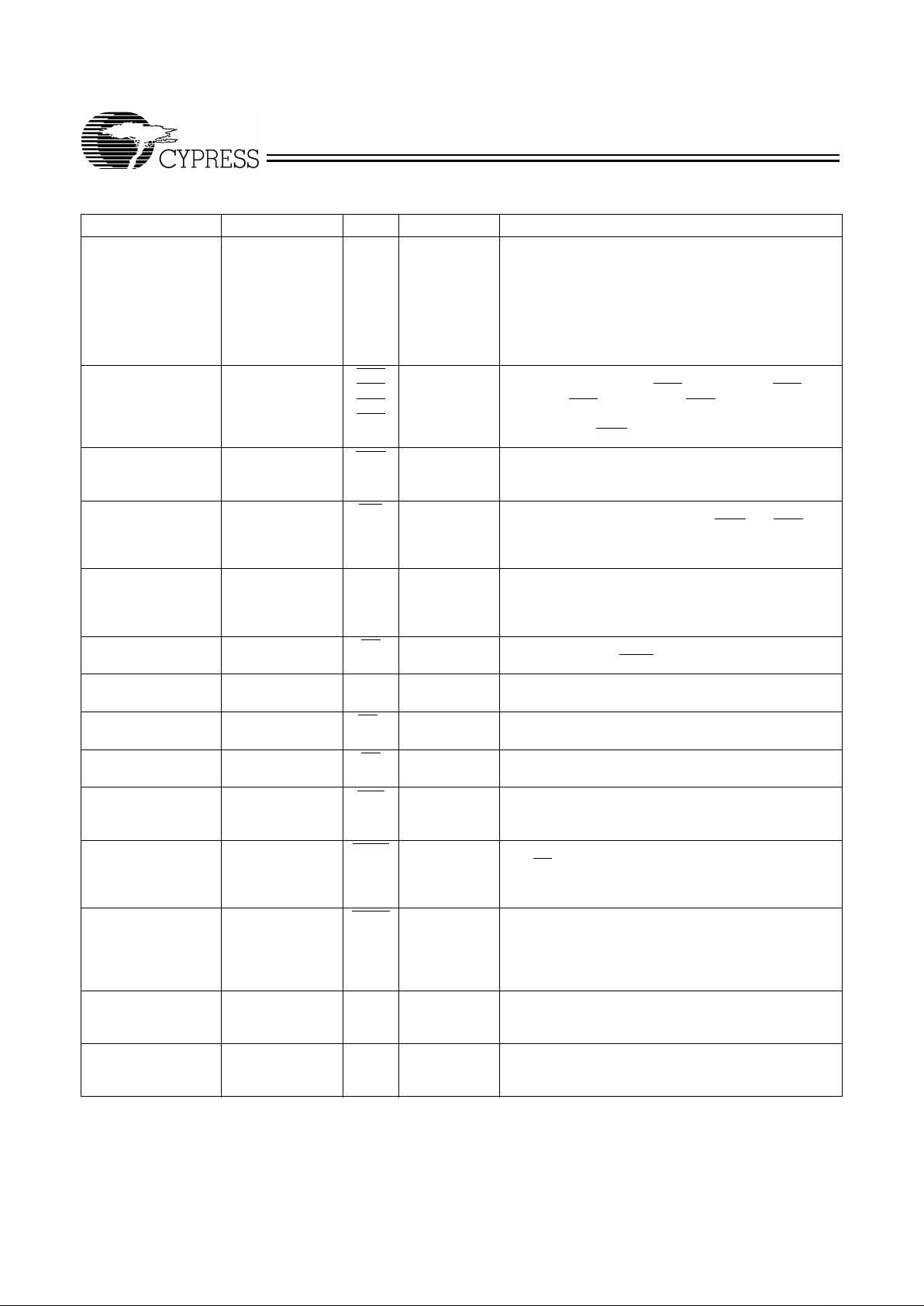
Notes:
1. The Functional Block Diagram illustrates simplified device operation. See Truth Table, pin descriptions and timing diagrams for detailed information.
2. CE
2
is for TA version only.
DQ
DQ
BWb#
BWE#
BWa#
GW#
BYTE b
WRITE
BYTE a
WRITE
OUTPUT
REGISTER
OE#
byte b write
ADSP#
ADSC#
Address
Register
Binary
Counter
& Logic
CLR
A
A1-A0
ADV#
MODE
512K x 9 x 2
SRAM Array
Output Buffers
Input
Register
byte a write
DQa,DQb
DQ DQ
DQ
ENABLE
Power Down LogicZZ
17
CE#
CE2
CE2#
DQ
DQ
BWc#
BWE#
BWd#
BYTE c WRITE
BYTE d WRITE
OUTPUT
REGISTER
OE#
byte c write
ADSP#
ADSC#
Address
Register
Binary
Counter
& Logic
CLR
A
A1-A0
ADV#
MODE
256K x 9 x 4
SRAM Array
Output Buffers
Input
Register
byte d write
DQa,DQb
DQc,DQd
DQ
DQ
DQ
BWa#
BWb#
GW#
BYTE a WRITE
BYTE b WRITE
CLK
byte b write
byte a write
DQ
DQ
ENABLE
Power Down LogicZZ
16
CE#
CE2
CE2#
Functional Block Diagram—256K x 36
[1]
Functional Block Diagram—512K x 18
[1]
[2]
[2]
CY7C1360A/GVT71256D36
CY7C1362A/GVT71512D18
PRELIMINARY
3
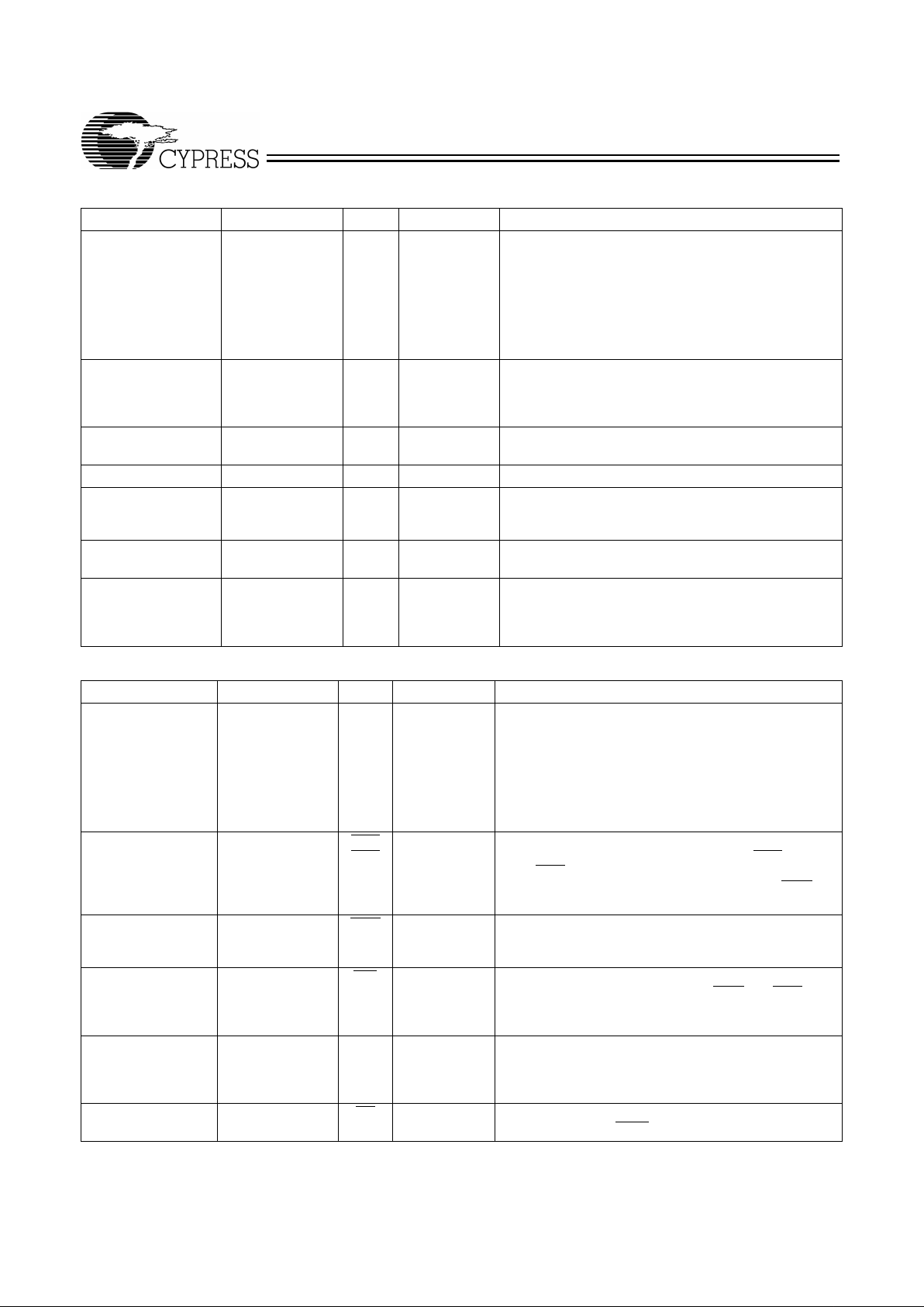
Pin Configurations
AAA
A
A1
A0
TMS
TDI
V
SS
V
CC
TDO
TCK
AAAAAAA
DQb
DQb
DQb
V
CCQ
V
SS
DQb
DQb
DQb
DQb
V
SS
V
CCQ
DQb
DQb
V
SS
NC
V
CC
ZZ
DQa
DQa
V
CCQ
V
SS
DQa
DQa
DQa
DQa
V
SS
V
CCQ
DQa
DQa
DQa
DQc
DQc
DQc
V
CCQ
V
SS
DQc
DQc
DQc
DQc
V
SS
V
CCQ
DQc
DQc
V
CC
NC
V
SS
DQd
DQd
V
CCQ
V
SS
DQd
DQd
DQd
DQd
V
SS
V
CCQ
DQd
DQd
DQd
A
A
CE
CE
2
BWd
BWc
BWb
BWa
A
VCCV
SS
CLKGWBWEOEADSC
ADSP
ADV
A
A
1
2
3
4
5
6
7
8
9
10
11
12
13
14
15
16
17
18
19
20
21
22
23
24
25
26
27
28
29
30
31323334353637383940414243444546474849
50
80
79
78
77
76
75
74
73
72
71
70
69
68
67
66
65
64
63
62
61
60
59
58
57
56
55
54
53
52
51
100999897969594939291908988878685848382
81
MODE
CY7C1360A/GVT71256D36
(256K X 36)
NC
A
NC
NC
V
CCQ
V
SS
NC
DPa
DQa
DQa
V
SS
V
CCQ
DQa
DQa
V
SS
NC
V
CC
ZZ
DQa
DQa
V
CCQ
V
SS
DQa
DQa
NC
NC
V
SS
V
DDQ
NC
NC
NC
NC
NC
NC
V
CCQ
V
SS
NC
NC
DQb
DQb
V
SS
V
CCQ
DQb
DQb
V
CC
NC
V
SS
DQb
DQb
V
CCQ
V
SS
DQb
DQb
DQb
NC
V
SS
V
CCQ
NC
NC
NC
AACE
CE2NCNCBWb
BWaAVCCV
SS
CLKGWBWEOEADSC
ADSP
ADV
A
A
1
2
3
4
5
6
7
8
9
10
11
12
13
14
15
16
17
18
19
20
21
22
23
24
25
26
27
28
29
30
31323334353637383940414243444546474849
50
80
79
78
77
76
75
74
73
72
71
70
69
68
67
66
65
64
63
62
61
60
59
58
57
56
55
54
53
52
51
100999897969594939291908988878685848382
81
CY7C1362A/GVT71512D18
(512K x 18)
NC
100-Pin TQFP
Top View
AAA
A
A1
A0
NC
NC
V
SS
V
CC
NC
AAAAAAA
A
DQb
DQb
DQb
V
CCQ
V
SS
DQb
DQb
DQb
DQb
V
SS
V
CCQ
DQb
DQb
V
SS
NC
V
CC
ZZ
DQa
DQa
V
CCQ
V
SS
DQa
DQa
DQa
DQa
V
SS
V
CCQ
DQa
DQa
DQa
DQc
DQc
DQc
V
CCQ
V
SS
DQc
DQc
DQc
DQc
V
SS
V
CCQ
DQc
DQc
V
CC
NC
V
SS
DQd
DQd
V
CCQ
V
SS
DQd
DQd
DQd
DQd
V
SS
V
CCQ
DQd
DQd
DQd
A
A
CE
CE
2
BWd
BWc
BWb
BWa
CE2VCCV
SS
CLKGWBWEOEADSC
ADSP
ADV
A
A
1
2
3
4
5
6
7
8
9
10
11
12
13
14
15
16
17
18
19
20
21
22
23
24
25
26
27
28
29
30
31323334353637383940414243444546474849
50
80
79
78
77
76
75
74
73
72
71
70
69
68
67
66
65
64
63
62
61
60
59
58
57
56
55
54
53
52
51
100999897969594939291908988878685848382
81
MODE
CY7C1360A/GVT71256D36
(256K X 36)
NC
A
NC
NC
V
CCQ
V
SS
NC
DQa
DQa
DQa
V
SS
V
CCQ
DQa
DQa
V
SS
NC
V
CC
ZZ
DQa
DQa
V
CCQ
V
SS
DQa
DQa
NC
NC
V
SS
V
CCQ
NC
NC
NC
NC
NC
NC
V
CCQ
V
SS
NC
NC
DQb
DQb
V
SS
V
CCQ
DQb
DQb
V
CC
NC
V
SS
DQb
DQb
V
CCQ
V
SS
DQb
DQb
DQb
NC
V
SS
V
CCQ
NC
NC
NC
AACE
CE2NCNCBWb
BWa
CE2VCCV
SS
CLKGWBWEOEADSC
ADSP
ADV
A
A
1
2
3
4
5
6
7
8
9
10
11
12
13
14
15
16
17
18
19
20
21
22
23
24
25
26
27
28
29
30
31323334353637383940414243444546474849
50
80
79
78
77
76
75
74
73
72
71
70
69
68
67
66
65
64
63
62
61
60
59
58
57
56
55
54
53
52
51
100999897969594939291908988878685848382
81
CY7C1362A/GVT71512D18
(512K x 18)
NC
TA Package Version
TA Package Version
T Package Version
T Package Version
AAA
A
A1
A0
TMS
TDI
V
SS
V
CC
TDO
TCK
AAAAAAA
MODE
AAA
A
A1
A0
NC
NC
V
SS
V
CC
NC
AAAAAAA
A
MODE
CY7C1360A/GVT71256D36
CY7C1362A/GVT71512D18
PRELIMINARY
4
Pin Configurations
(continued)
119-Ball BGA
1234567
A V
CCQ
A A ADSP AAV
CCQ
B NC CE
2
AADSCAANC
C NC A A V
CC
AANC
D DQc DQc V
SS
NC V
SS
DQb DQb
E DQc DQc V
SS
CE V
SS
DQb DQb
F V
CCQ
DQc V
SS
OE V
SS
DQb V
CCQ
G DQc DQc BWc
ADV BWb DQb DQb
H DQc DQc V
SS
GW V
SS
DQb DQb
J V
CCQ
V
CC
NC V
CC
NC V
CC
V
CCQ
K DQd DQd V
SS
CLK V
SS
DQa DQa
L DQd DQd BWd
NC BWa DQa DQa
M V
CCQ
DQd V
SS
BWE V
SS
DQa V
CCQ
N DQd DQd V
SS
A1 V
SS
DQa DQa
P DQd DQd V
SS
A0 V
SS
DQa DQa
R NC A MODE V
CC
NC A NC
T NC NC A A A NC ZZ
U V
CCQ
TMS TDI TCK TDO NC V
CCQ
Top View
1234567
A V
CCQ
A A ADSP AAV
CCQ
B NC CE
2
AADSCACE2NC
C NC A A V
CC
AANC
D DQb NC V
SS
NC V
SS
DQa NC
E NC DQb V
SS
CE V
SS
NC DQa
F V
CCQ
NC V
SS
OE V
SS
DQa V
CCQ
G NC DQb BWb
ADV V
SS
NC DQa
H DQb NC V
SS
GW V
SS
DQa NC
J V
CCQ
V
CC
NC V
CC
NC V
CC
V
CCQ
K NC DQb V
SS
CLK V
SS
NC DQa
L DQb NC V
SS
NC BWa DQa NC
M V
CCQ
DQb V
SS
BWE V
SS
NC V
CCQ
N DQb NC V
SS
A1 V
SS
DQa NC
P NC DQb V
SS
A0 V
SS
NC DQa
R NC A MODE V
CC
NC A NC
T NC A A NC A A ZZ
U V
CCQ
TMS TDI TCK TDO NC V
CCQ
256Kx36
512Kx18
CY7C1360A/GVT71256D36
CY7C1362A/GVT71512D18
PRELIMINARY
5
256K X 36 Pin Descriptions
X36 PBGA Pins X36 QFP Pins Name Type Description
4P
4N
2A, 3A, 5A, 6A, 3B,
5B, 6B, 2C, 3C, 5C,
6C, 2R, 6R, 3T, 4T, 5T
37
36
35, 34, 33, 32,
100, 99, 82, 81,
44, 45, 46, 47, 48,
49, 50
92 (T Version)
43 (TA Version)
A0
A1
A
Input-
Synchronous
Addresses: These inpu ts a re regis tered a nd m ust me et
the set-up and hold times arou nd the rising edge of CLK.
The burst counter generates internal addresses associated with A0 and A1, during burst cycle and wait cycle.
5L
5G
3G
3L
93
94
95
96
BWa
BWb
BWc
BWd
Input-
Synchronous
Byte Write: A byte write is LOW for a WRITE cycle and
HIGH for a READ cycle. BWa
controls DQa. BWb controls DQb. BWc c ontrols D Qc. BW d controls DQd. Data
I/O are high impedanc e if either of these in puts are LOW ,
conditioned by BWE
being LOW.
4M 87 BWE
Input-
Synchronous
Write Enable: This active LOW input gates byte write
operations and must meet the set-up and hold times
around the rising edge of CLK.
4H 88 GW
Input-
Synchronous
Global Write: This active LOW input allows a full 36-bit
WRITE to occur independ ent of the BWE
and BWn lines
and must meet the set-up and hold times around the
rising edge of CLK.
4K 89 CLK Input-
Synchronous
Clock: This signal registers the addresses, data, chip
enables , write control, and burst c ontrol inputs on its rising edge. All synchron ous inp uts m ust m eet set-u p and
hold times around the clock’s rising edge.
4E 98 CE
Input-
Synchronous
Chip Enable: Th is active LO W input is used to enable the
device and to gate ADSP
.
2B 97 CE
2
Input-
Synchronous
Chip Enable: This active HIGH input is used to enable
the device.
- (not availab le for
PBGA)
92 (for TA Version
only)
CE
2
Input-
Synchronous
Chip Enable: Th is active LO W input is used to enable the
device. Not available for B and T package versions.
4F 86 OE
Input Output Enable: This a ctive LO W asynch ronous input en-
ables the data output drivers.
4G 83 ADV
Input-
Synchronous
Address Advance : This activ e LO W input is us ed to control the internal burst co unter. A HIGH on this pin generates wait cycle (no address advance).
4A 84 ADSP
Input-
Synchronous
Address Status Processo r: This active LO W input, along
with CE
being LOW, causes a new external address to
be registered and a READ cycle i s initiated using the new
address.
4B 85 ADSC
Input-
Synchronous
Address Status Controller: This active LOW input causes the device to be deselected or selected along with
new external address to be registered. A READ or
WRITE cycle is initiated depending upon write control
inputs.
3R 31 MODE Input-
Static
Mode: This input sele cts the b urst seq uence. A L OW on
this pin selects Linear Burst. A NC or HIGH on this pin
selects Interleaved Burst.
7T 64 ZZ Input-
Asynchronous
Snooze: This active HIGH input puts the device in low
power consumption standby mode. For normal operation, this input has to be e ither LOW or NC (N o Connect).
CY7C1360A/GVT71256D36
CY7C1362A/GVT71512D18
PRELIMINARY
6
(a) 6P, 7P, 7N, 6N,
6M, 6L, 7L, 6K, 7K,
(b) 7H, 6H, 7G, 6G,
6F, 6E, 7E, 7D, 6D,
(c) 2D , 1D, 1E, 2E, 2F,
1G, 2G, 1H, 2H,
(d) 1K, 2K, 1L, 2L,
2M, 1N, 2N, 1P, 2P
(a) 51, 52, 53, 56,
57, 58, 59, 62, 63
(b) 68, 69, 72, 73,
74, 75, 78, 79, 80
(c) 1, 2, 3, 6, 7, 8,
9, 12, 13
(d) 18, 19, 22, 23,
24, 25, 28, 29, 30
DQa
DQb
DQc
DQd
Input/
Output
Data Inputs/Outputs: First By te i s DQa. Se co nd By te i s
DQb. Third Byt e is DQc. F ourth Byte is DQd. Input data
must meet set-up and hol d times around the rising edge
of CLK.
2U
3U
4U
38
39
43
for B and T v ersion
TMS
TDI
TCK
Input IEEE 1149.1 test inputs. LVTTL-level inputs. Not avail-
able for TA package version.
5U 42
for B and T v ersion
TDO Output IEEE 1149.1 test output. LVTTL-level output. Not avail-
able for TA package version.
4C, 2J, 4J, 6J, 4R 15, 41, 65, 91 V
CC
Supply Core power Supply: +3.3V –5% and +10%
3D , 5D, 3E, 5E, 3F , 5F,
3H, 5H, 3K, 5K, 3M,
5M, 3N, 5N, 3P, 5P
5, 10, 17, 21, 26,
40, 55, 60, 67, 71,
76, 90
V
SS
Ground Ground: GND.
1A, 7A, 1F, 7F , 1J , 7J,
1M, 7M, 1U, 7U
4, 11, 20, 27, 54,
61, 70, 77
V
CCQ
I/O Supply Output Buffer Supply: +2.5V or +3.3V.
1B, 7B, 1C, 7C, 4D,
3J, 5J, 4L, 1R, 5R,
7R, 1T, 2T, 6T, 6U
14, 16, 66
38, 39, 42 for TA
Version
NC - No Connect: These sig nals are not internally conne cted.
User can leave it floating or connect it to V
CC
or VSS.
256K X 36 Pin Descriptions
(continued)
X36 PBGA Pins X36 QFP Pins Name Type Description
512K X 18 Pin Descriptions
X18 PBGA Pins X18 QFP Pins Name Type Description
4P
4N
2A, 3A, 5A, 6A, 3B,
5B, 6B, 2C, 3C, 5C,
6C, 2R, 6R, 2T, 3T,
5T, 6T
37
36
35, 34, 33, 32,
100, 99, 82, 81,
80, 48, 47, 46, 45,
44, 49, 50
92 (T Version)
43 (TA Version)
A0
A1
A
Input-
Synchronous
Addresses: These inputs are registered and must meet
the set up and hold t imes ar ound the rising ed ge of C LK.
The burst counter generates internal addresses associated with A0 and A1, during burst cycle and wait cycle.
5L
3G
93
94
BWa
BWb
Input-
Synchronous
Byte Write Enables: A byte write enable is LOW for a
WRITE cycle and HIGH for a READ cycle. BW a
controls
DQa. BWb controls DQb . Data I/O ar e high impedanc e if
either of these inputs are LOW, conditioned by BWE
be-
ing LOW.
4M 87 BWE
Input-
Synchronous
Write Enable: This active LOW input gates byte write operations and mus t meet the set-up and hold times aro und
the rising edge of CLK.
4H 88 GW
Input-
Synchronous
Global Write: This active LOW input allows a full 18-bit
WRITE to occur inde pendent o f the BWE
and WEn lines
and must meet the set-up and hold times around the rising edge of CLK.
4K 89 CLK Input-
Synchronous
Clock: This signa l registers the addres ses, data, ch ip enables, write control and burst control inputs on its rising
edge. All sync hronous inputs m ust mee t set- up and h old
times around the clock’s rising edge.
4E 98 CE
Input-
Synchronous
Chip Enable: This active LOW input is used to enable the
device and to gate ADSP
.
CY7C1360A/GVT71256D36
CY7C1362A/GVT71512D18
PRELIMINARY
7
2B 97 CE2 Input-
Synchronous
Chip Enable: This active HIGH input is use d to enable the
device.
- (not available for
PBGA)
92 (for TA Versio n
only)
CE2 Input-
Synchronous
Chip Enable: This active LOW input is used to enable the
device. Not available for B and T package versions.
4F 86 OE
Input Output Enable: Thi s activ e LOW asynchronous input en-
ables the data output drivers.
4G 83 ADV
Input-
Synchronous
Address Adva nc e: T his ac tive LOW input is used to c ontrol the internal burst counter. A HIGH on this pin generates wait cycle (no address advance).
4A 84 ADSP
Input-
Synchronous
Address Status Processor: This act ive LO W in put, along
with CE
being LOW , ca uses a new ex ternal address to be
registered and a READ cycle is initiated using the new
address.
4B 85 ADSC
Input-
Synchronous
Address Status Cont roller: This activ e LOW input causes
device to be de selected or se lected along with ne w e xternal address to be registere d. A READ or WRI TE cycle i s
initiated depending upon write control inputs.
3R 31 MODE Input-
Static
Mode: This inpu t se lec ts th e burst sequence. A LOW on
this pin selects Linear Burst. An NC or HIGH on this pi n
selects Interleaved Burst.
7T 64 ZZ Input-
Asynchronous
Snooze: This active HIGH input puts the device in low
power consump tion standby mode. F or normal operation,
this input has to be either LOW or NC (No Connect).
(a) 6D, 7E, 6F, 7G,
6H, 7K, 6L, 6N, 7P
(b) 1D, 2E, 2G, 1H,
2K, 1L, 2M, 1N, 2P
(a) 58, 59, 62, 63,
68, 69, 72, 73, 74
(b) 8, 9, 12, 13, 18,
19, 22, 23, 24
DQa
DQb
Input/
Output
Data Inputs/Outputs: Lo w Byte is DQa. High Byte is DQb.
Input data must meet set up and hold times around the
rising edge of CLK.
2U
3U
4U
38
39
43
for B and T v ersion
TMS
TDI
TCK
Input IEEE 1149.1 test inputs. LVTTL-level inputs . Not available
for TA package version.
5U 42
for B and T v ersion
TDO Output IEEE 1149.1 test output. LVTTL-level output. Not avail-
able for TA package version.
4C, 2J, 4J, 6J, 4R 15, 41,65, 91 V
CC
Supply Core power Supply: +3.3V –5% and +10%
3D, 5D, 3E, 5E, 3F,
5F, 5G, 3H, 5H, 3K,
5K, 3L, 3M, 5M, 3N,
5N, 3P, 5P
5, 10, 17, 21, 26,
40, 55, 60, 67, 71,
76, 90
V
SS
Ground Ground: GND.
1A, 7A, 1F , 7 F , 1J, 7J ,
1M, 7M, 1U, 7U
4, 11, 20, 27, 54,
61, 70, 77
V
CCQ
I/O Supply Output Buffer Supply: +2.5V or +3.3V.
1B, 7B, 1C, 7C, 2D,
4D, 7D, 1E, 6E, 2F,
1G, 6G, 2H, 7H, 3J,
5J, 1K, 6K, 2L, 4L,
7L, 6M, 2N, 7N, 1P,
6P, 1R, 5R, 7R, 1T,
4T, 6U
1–3, 6, 7, 14, 16,
25, 28–30, 51–53,
56, 57, 66, 75, 78,
79, 80, 95, 96
38, 39, 42 for TA
Version
NC - No Connect: These signals are not internally connected.
User can leave it floating or connect it to V
CC
or VSS.
512K X 18 Pin Descriptions
(continued)
X18 PBGA Pins X18 QFP Pins Name Type Description
CY7C1360A/GVT71256D36
CY7C1362A/GVT71512D18
PRELIMINARY
8
Notes:
3. X = “Don’t Care.” H = logic HIGH. L = logic LOW.
For X36 product, WRITE
= L means [BWE + BWa*BWb*BWc*BWd]*GW equals LOW. WRITE = H means [BWE + BWa*BWb*BWc*BWd]*GW equals HIGH.
For X18 product, WRITE = L means [BWE + BWa*BWb]*GW equals LOW. WRITE = H means [BWE + BWa*BWb]*GW equals HIGH.
4. BWa
enables write to DQa. BWb enables write to DQb. BWc enables write to DQ c. BWd ena bles wri te to DQd.
5. All inputs except OE must meet set up and hold times around the rising edge (LOW to HIGH) of CLK.
6. Suspending burst generates wait cycle.l
7. For a write operation following a read operation, OE
must be HI GH befo re the in put data re quired set -up time plus High- Z time f or OE and staying HIGH throughout
the input data hold time.
8. This device contains circuitry that will ensure the outputs will be in High-Z during power-up.
9. ADSP
LOW along with chip being selected always initiates a READ cycle at the L-H edge of CLK. A WRITE cycle can be performed by setting WRITE LOW for
the CLK L-H edge of the subsequent wait cycle. Refer to WRITE timing diagram for clarification.
Burst Address Table (MODE = NC/VCC)
First
Address
(external)
Second
Address
(internal)
Third
Address
(internal)
Fourth
Address
(internal)
A...A00 A...A01 A...A10 A...A11
A...A01 A...A00 A...A11 A...A10
A...A10 A...A11 A...A00 A...A01
A...A11 A...A10 A...A01 A...A00
Burst Address Table (MODE = GND)
First
Address
(external)
Second
Address
(internal)
Third
Address
(internal)
Fourth
Address
(internal)
A...A00 A...A01 A...A10 A...A11
A...A01 A...A10 A...A11 A...A00
A...A10 A...A11 A...A00 A...A01
A...A11 A...A00 A...A01 A...A10
Truth Table
[3, 4, 5, 6, 7, 8, 9]
Operation Address Used CE CE2 CE2 ADSP ADSC ADV WRITE OE CLK DQ
Deselected Cycle, Power Down None H X X X L X X X L-H High-Z
Deselected Cycle, Power Down None L X L L X X X X L-H High-Z
Deselected Cycle, Power Down None L H X L X X X X L-H High-Z
Deselected Cycle, Power Down None L X L H L X X X L-H High-Z
Deselected Cycle, Power Down None L H X H L X X X L-H High-Z
READ Cycle, Begin Burst External L L H L X X X L L-H Q
READ Cycle, Begin Burst External L L H L X X X H L-H High-Z
WRITE Cycle, Begin Burst External L L H H L X L X L-H D
READ Cycle, Begin Burst External L L H H L X H L L-H Q
READ Cycle, Begin Burst External L L H H L X H H L-H High-Z
READ Cycle, Continue Burst Next X X X H H L H L L-H Q
READ Cycle, Continue Burst Next X X X H H L H H L-H High-Z
READ Cycle, Continue Burst Next H X X X H L H L L-H Q
READ Cycle, Continue Burst Next H X X X H L H H L-H High-Z
WRITE Cycle, Continue Burst Next X X X H H L L X L-H D
WRITE Cycle, Continue Burst Next H X X X H L L X L-H D
READ Cycle, Suspend Burst Current X X X H H H H L L-H Q
READ Cycle, Suspend Burst Current X X X H H H H H L-H High-Z
READ Cycle, Suspend Burst Current H X X X H H H L L-H Q
READ Cycle, Suspend Burst Current H X X X H H H H L-H High-Z
WRITE Cycle, Suspend Burst Current X X X H H H L X L-H D
WRITE Cycle, Suspend Burst Current H X X X H H L X L-H D

CY7C1360A/GVT71256D36
CY7C1362A/GVT71512D18
PRELIMINARY
9
IEEE 1149.1 Serial Boundary Scan (JTAG)
Overview
This device incorporates a serial boundary scan access port
(TAP). This port is designed to operate in a man ner consi stent
with IEEE Standard 1149.1-1990 (commonly referred to as
JTAG), but d oes not im plement al l of th e func tions re quired for
IEEE 1149.1 compliance. Certain functions have been modified or eliminated because their implementation places extra
delays in the critical speed path of the device. Nevertheless,
the device supports the standard TAP controller architecture
(the TAP controller is the state m achin e tha t cont rols t he TAPs
operation) and can be expected to function in a manner that
does not conflict with the o pera tion of de vice s with IEEE Standard 1149.1 compliant TAPs. The TAP operates using LVTTL/
LVCMOS logic level signaling.
Disabling the JTAG Feature
It is possib le to use this de v ice witho ut using the JTAG feature .
To disable t he TAP contro ller without i nterfering with no rmal
operation of the de vice , TCK shou ld be tied LO W (V
SS
) to prevent cloc king the d e vice . TDI and TMS ar e internally pulled up
and may be unconnected. They may alternately be pulled up
to V
CC
through a resistor. TDO should be left unconnected.
Upon power-up the device will come up in a reset state which
will not interfere w ith the ope r ati on of the device.
Test Access Port (TAP)
TCK - Test Clock (INPUT)
Clocks all TAP events. All inputs are captured on the rising
edge of TCK and all outp uts propagate fr om the f alling edge of
TCK.
TMS - Test Mode Select (INPUT)
The TMS input is sampled on the rising edge of TCK. This is
the command input for the TAP controller state machine. It is
allowab le to lea ve this pin unconnected if the TAP is not used.
The pin is pulled up internally, resulting in a logic HIGH level.
TDI - Test Data In (INPUT)
The TDI input is samp led on the rising edge o f TCK. This is the
input side of the se rial registers pl aced betwe en TDI and TDO .
The register placed between TDI and TDO is determined by
the state of the TAP controller state machine and the instruction that is currentl y loaded in the TAP instruction register (ref er
to Figure 1, TAP Controller State Diagram). It is allowable to
leave this pin unconnected if it is not used in an application.
The pin is pulled up inter nally, resulting in a logic HIGH level.
TDI is connected to th e M ost Si gn ific an t Bi t (M SB) o f a n y re gister. (See Figure 2.)
TDO - Test Data Out (OUTPUT)
The TDO output pin i s use d to seri all y clo ck data-out from the
registers. The output that is active depending on the state of
the TAP state machine (ref er to Figure 1, TAP Controller State
Diagram). Output changes in response to the falling edge of
TCK. This is the output side of the serial regi sters placed between TDI and TDO . TDO is conne cted to the Least Significa nt
Bit (LSB) of any register. (See Figure 2.)
Performing a TAP Reset
The TAP circuitry does not have a reset pin (TRST
, which is
optional in the IEEE 1149.1 specification). A RESET can be
performed for the TAP controller by forcing TMS HIGH (V
CC
)
for five rising edges of TCK and pre-loads the instruction register with the IDCODE command. This type of reset does not
affect the operation of the system logic. The reset affects test
logic only.
At power-up, the TAP is reset internally to ensure that TDO is
in a High-Z state.
Test Access Port (TAP) Registers
Overview
The various TAP registers are selected (one at a time) via the
sequences of ones and z eros inpu t to the TMS pin a s the TC K
is strobed. Each of the TAPs registers are serial shift register s
that capture serial input data on the rising edge of TCK and
push serial data out on subseque nt f alling edge of TCK. Whe n
a register is selected, it is connected between the TDI and
TDO pins.
Instruction Register
The instruction register holds the instructions that are executed by the TAP controller when it is moved into the run test/idl e
or the various data register states. The instructions are three
bits long. The register c an be loaded when it is placed between
the TDI and TDO pins. The parallel outputs of the instruction
register are automaticall y preloaded with th e IDCODE instruction upon powe r-up or whenever the controller is placed in th e
test-logic reset state. When the TAP controller is in the Capture-IR state, the two least si gnifican t bits of the serial instruction register are loaded with a binary “01” pattern to allow for
fault isolation of the board-level serial test data path.
Bypass Register
The bypass register is a single-bit register that can be placed
between TDI and TDO. It allows serial test data to be passed
through the device TAP to another device in the scan chain
with minimum del ay. The bypass register is set LOW (V
SS
)
when the BYPASS instruction is executed.
Note:
10. For the X18 product, there are only BWa
and BWb.
Partial Truth Table for READ/WRITE
[10]
Function GW BWE BWa BWb BWc BWd
READ H H X X X X
READ H L H H H H
WRITE one byte H L L H H H
WRITE all bytes H L L L L L
WRITE all bytes L X X X X X

CY7C1360A/GVT71256D36
CY7C1362A/GVT71512D18
PRELIMINARY
10
Boundary Scan Register
The Boundary Scan register is connected to all the input and
bidirectional I/O pins (not counting the TAP pins) on the device.
This also incl udes a number of NC pins th at are r eser ved for
future needs. Ther e are a total of 70 bits f or the x36 de vice and
51 bits for the x18 device. The boundary scan register, under
the control of the TAP controller, is loaded with the conten ts of
the device I/O ring when the controller is in Capture-DR state
and then is placed between the TDI and TDO pins when the
controller is moved to Shift-DR state. The EXTEST, SAMPLE/PRELOAD and SAMPLE-Z instructions can be used to
capture the contents of the I/O ring.
The Boundary Scan Order table describes the order in which
the bits are connecte d. Th e fir st c olu mn defi nes the bit’s position in the boundary scan register. The MSB of the register is
connected to TDI, and LSB is connected to TDO. The second
column is the signal name, the third column is the TQFP pin
number, and the fourth column is the BGA bump number.
Identification (ID) Register
The ID Register is a 32-bi t register that is loaded with a de vice
and vendor specific 32-bit code when the controller is put in
Capture-DR state with the IDCODE command loaded in the
instruction register. The register is then placed between the
TDI and TDO pins when the controller is moved into Shift-DR
state. Bit 0 in the r egister i s the LSB an d the fi rst to rea ch TDO
when shifting b egins . The c ode is loaded from a 32-b it on- chip
ROM. It desc ribes various att ributes of the de vice as desc ribed
in the Identification Register Definitions table.
TAP Controller Instruction Set
Overview
There are two clas ses of instructions defined in the I EEE Standard 1149.1 -1990; the standard ( public) ins tructio ns and device specific (private) instructions. Some public instructions
are mandatory for IEEE 1149.1 compliance. Optional public
instructions must be implemented in prescribed ways.
Although the TAP controller in this device follows the IEEE
1149.1 conventions, it is not IEEE 1149.1 compliant because
some of the manda tory instructions are no t fully im plemente d.
The TAP on this device may be used to monitor all input and
I/O pads, b u t can not b e us ed to load addres s , data, or co ntrol
signals into the device or to preload the I/O buffers. In other
words, the device will not perform IEEE 1149.1 EXTEST, INTEST, or the preload portion of the SAMPLE/PRELOAD command.
When the TAP controller is place d in Capture-IR state, the two
least significant bits of the instruction register are loaded with
01. When the controller is moved to the Shift-IR state the instruction is serially loaded through the TDI input (while the
previous c ontents are shifted out at TDO). F or a ll ins tructions,
the T AP e xecutes ne wly loaded instruction s only when the controller is moved to Update-IR state. The TAP instruction sets
for this device are listed in the following tables.
EXTEST
EXTEST is an IEEE 1149.1 mandatory public instruction. It is
to be ex ecuted w hene ver th e instruction register is lo aded with
all 0s. EXTEST is not implemented in this device.
The TAP controller does recognize an all-0 instruction. When
an EXTEST instruction is loaded into the instruction register,
the device responds as if a SAMPLE/PRELOAD instruction
has been loaded. There is one diff erence between tw o instructions. Unlike SAMPLE/PRELO AD instruction, EXTEST places
the device outputs in a High-Z state.
IDCODE
The IDCODE instruction c auses a vend or-specific , 32-bit code
to be loaded into th e ID re gis ter when the controller is in Ca pture-DR mode and places the ID register betw een the TDI and
TDO pins in Shift-DR mode. The IDCODE instruction is the
default in struction loaded in the instruction upon po wer-up and
at any time the TAP controller is placed in the test-logic reset
state.
SAMPLE-Z
If the High-Z instructio n is l oaded in th e inst ruction reg ister, all
output pins are f orced to a High-Z state a nd the boundary scan
register is connected between TDI and TDO pins when the
TAP controller is in a Shift-DR state.
SAMPLE/PRELOAD
SAMPLE/PRELOAD is an IEEE 1149.1 man datory instruction.
The PRELOAD portion of the command is not imple mented in
this device, so the device TAP controller is not fully IEEE
1149.1-compliant.
When the SAMPLE/PRELOAD instruction is loaded in the in-
struction register and the TAP controller is in the Capture-DR
state, a snap shot of the data in the device’s input and I/O
buff ers is loa ded into the boundary scan reg ister. Because the
device system clock(s) are independent from the TAP clock
(TCK), it is possib le for the TAP to attempt to capture the inp ut
and I/O ring contents while the buffers are in trans ition (i.e., in
a metastable state). Although allowing the TAP to sample
metastable inputs will not harm the device, repeatable results
can not be expected. To guarantee that the boundary scan
register will capture the correct value of a signal, the device
input signals must be stabilized long enough to meet the TAP
controller’s capture set up plus hold time (t
CS
plus tCH). The
device clock input(s) need not be paused for any other TAP
operation e xcept c apturing the input and I/O ring content s into
the boundary scan register.
Moving the controller to Shift-DR state then places the boundary scan register betwee n the TDI and TDO pins . Because th e
PRELOAD portion of the command i s n ot i mp lemen ted in thi s
device, moving the controller to the Update-DR state with the
SAMPLE/PRELOAD instruction loaded in the instruction register has the same effect as the Pause-DR command.
BYPASS
When the BYPASS instruction is loaded in the instruction register and the TAP controller is in the Shift-D R state, the b ypass
register is placed betwe en TDI and TDO . This allows the boa rd
level scan path to be shortened to facilitate testing of other
devices in the scan pat h.
Reserved
Do not use these instructions. They are reserved for future
use.

CY7C1360A/GVT71256D36
CY7C1362A/GVT71512D18
PRELIMINARY
11
Note:
11. The 0/1 next to each state represents the value at TMS at the rising edge of TCK.
Figure 1. TAP Controller State Diagram
[11]
TEST-LOGIC
RESET
REUN-TEST/
IDLE
SELECT
DR-SCAN
CAPTURE-DR
SHIFT-DR
EXIT1-DR
PAUSE-DR
EXIT2-DR
UPDATE-DR
SELECT
IR-SCAN
CAPTURE-IR
SHIFT-IR
EXIT1-IR
PAUSE-IR
EXIT2-IR
UPDATE-IR
1
0
1
1
0
1
0
1
0
0
0
1
1
1
0
1
0
1
0
0
0
1
0
1
1
0
1
0
0
1
1
0

CY7C1360A/GVT71256D36
CY7C1362A/GVT71512D18
PRELIMINARY
12
Figure 2. TAP Controller Block Diagram
0
012..
29
3031
Boundary Scan Register
Identification Register
012..
.
.x
012
Instruction Register
Bypass Register
Selection
Circuitry
Selection
Circuitry
TAP Controller
TDI
TDO
TDI
TDI
[12]
TAP Electrical Characteristics (20°C < T
j
< 110°C; VCC = 3.3V –0.2V and +0.3V unless otherwise noted)
Parameter Description Test Conditions Min. Max. Unit
V
IH
Input High (Logic 1) Voltage
[13, 14]
2.0 VCC + 0.3 V
V
Il
Input Low (Logic 0) Voltage
[13, 14]
–0.3 0.8 V
IL
I
Input Leakage Current 0V < VIN < VCC –5.0 5.0 µA
IL
I
TMS and TDI Input Leakage Current 0V < VIN < VCC –30 30 µA
IL
O
Output Leakage Current Output disabled,
0V < VIN < V
CCQ
–5.0 5.0 µA
V
OLC
LVCMOS Output Low Voltage
[13, 15]
I
OLC
= 100 µA 0.2 V
V
OHC
LVCMOS Output High Voltage
[13, 15]
I
OHC
= 100 µA VCC – 0.2 V
V
OLT
LVTTL Output Low Voltage
[13]
I
OLT
= 8.0 mA 0.4 V
V
OHT
LVTTL Output High Voltage
[13]
I
OHT
= 8.0 mA 2.4 V
Notes:
12. X = 69 for the x36 configuration;
X = 50 for the x18 configuration.
13. All Voltage referenced to V
SS
(GND).
14. Overshoot: V
IH
(AC)<V
CC
+1.5V for t<
t
KHKH
/2, Undershoot: VIL(AC)<–0.5V for t<t
KHKH
/2, Power-up: VIH<3.6V and VCC<3.135V and V
CCQ
<1.4V for t<200 ms.
During normal operation, V
CCQ
must not exceed VCC. Control input signals (such as R/W, ADV/LD, etc.) may not have pulse widths less than t
KHKL
(min.).
15. This parameter is sampled.

CY7C1360A/GVT71256D36
CY7C1362A/GVT71512D18
PRELIMINARY
13
TAP AC Switching Characteristics
Over the Oper at ing Rang e
[16, 17]
Parameter Description Min. Max Unit
Clock
t
THTH
Clock Cycle Time 20 ns
f
TF
Clock Frequency 50 MHz
t
THTL
Clock HIGH Time 8 ns
t
TLTH
Clock LOW Time 8 ns
Output Times
t
TLQX
TCK LOW to TDO Unknown 0 ns
t
TLQV
TCK LOW to TDO Valid 10 ns
t
DVTH
TDI Valid to TCK HIGH 5 ns
t
THDX
TCK HIGH to TDI Invalid 5 ns
Set-up Times
t
MVTH
TMS Set-up 5 ns
t
CS
Capture Set-up 5 ns
Hold Times
t
THMX
TMS Hold 5 ns
t
CH
Capture Hold 5 ns
Notes:
16. t
CS
and tCH refer to the set-up and hold time requirements of latching data from the boundary scan register.
17. Test conditions are specified using the load in TAP A C test conditions.

CY7C1360A/GVT71256D36
CY7C1362A/GVT71512D18
PRELIMINARY
14
TAP Timing and Test Conditions
(a)
3.0V
V
SS
ALL INPUT PULSES
1.5V
(b)
1.5 ns
1.5 ns
TEST CLOCK
(TCK)
t
THTH
t
THTL
t
TLTH
TEST MODE SELECT
(TMS)
TEST DATA IN
(TDI)
TEST DATA OUT
(TDO)
t
MVTHtTHMX
t
DVTH
t
THDX
t
TLQX
t
TLQV
Vt = 1.5V
TDO
Z
0
= 50
Ω
50
Ω
20 pF

CY7C1360A/GVT71256D36
CY7C1362A/GVT71512D18
PRELIMINARY
15
Identification Register Definiti ons
Instruction Field 256K x 36 512K x 18 Description
REVISION NUMBER
(31:28)
XXXX XXXX Reserved for revision number.
DEVICE DEPTH
(27:23)
00110 00111 Defines depth of 256K or 512K words.
DEVICE WIDTH
(22:18)
00100 00011 Defines width of x36 or x18 bits.
RESERVED
(17:12)
XXXXXX XXXXXX Reserved for future use.
CYPRESS JEDEC ID
CODE (11:1)
00011100100 00011100100 Allows unique identification of DEVICE vendor.
ID Register Presence
Indicator (0)
1 1 Indicates the presence of an ID register.
Scan Register Sizes
Register Name Bit Size (x36) Bit Size (x18)
Instruction 3 3
Bypass 1 1
ID 32 32
Boundary Scan 70 51
Instruction Codes
Instruction Code Description
EXTEST 000 Captures I/O ring contents. Place s the bounda ry scan register betw een TDI
and TDO. Forces all device outputs to High-Z state. This instruction is not
IEEE 1149.1-compliant.
IDCODE 001 Preloads ID register with vendor ID code and places it between TDI and
TDO. This instruction does not affect device operations.
SAMPLE-Z 010 Captures I/O ring contents. Place s the bounda ry scan register betw een TDI
and TDO. Forces all device outputs to High-Z state.
RESERVED 011 Do not use these instructions; they are reserved for future use.
SAMPLE/PRELOAD 100 Captures I/O ring contents. Place s the bounda ry scan register betw een TDI
and TDO. This instruction do es not aff ect de vice oper ations. Thi s instruction
does not implement IEEE 1149.1 PRELOAD function and is therefore not
1149.1-compliant.
RESERVED 101 Do not use these instructions; they are reserved for future use.
RESERVED 110 Do not use these instructions; they are reserved for future use.
BYPASS 111 Places the by pass registe r between TDI and TDO . Thi s instruction doe s not
affect device operations.

CY7C1360A/GVT71256D36
CY7C1362A/GVT71512D18
PRELIMINARY
16
Boundary Scan Order (256K x 36)
Bit#
Signal
Name TQFP Bump ID
1 A 44 2R
2 A 45 3T
3 A 46 4T
4 A 47 5T
5 A 48 6R
6 A 49 3B
7 A 50 5B
8 DQa 51 6P
9 DQa 52 7N
10DQa536M
11 DQa 56 7L
12 DQa 57 6K
13 DQa 58 7P
14 DQa 59 6N
15 DQa 62 6L
16 DQa 63 7K
17 ZZ 64 7T
18 DQb 68 6H
19 DQb 69 7G
20 DQb 72 6F
21 DQb 73 7E
22 DQb 74 6D
23 DQb 75 7H
24 DQb 78 6G
25 DQb 79 6E
26 DQb 80 7D
27 A 81 6A
28 A 82 5A
29 ADV
83 4G
30 ADSP
84 4A
31 ADSC
85 4B
32 OE
86 4F
33 BWE
87 4M
34 GW
88 4H
35 CLK 89 4K
36 A 92 6B
37 BWa
93 5L
38 BWb
94 5G
39 BWc
95 3G
40 BWd
96 3L
41 CE
2
97 2B
42 CE
98 4E
43 A 99 3A
44 A 100 2A
45 DQc 1 2D
46 DQc 2 1E
47 DQc 3 2F
48 DQc 6 1G
49 DQc 7 2H
50 DQc 8 1D
51 DQc 9 2E
52 DQc 12 2G
53 DQc 13 1H
54 NC 14 5R
55 DQd 18 2K
56 DQd 19 1L
57DQd222M
58 DQd 23 1N
59 DQd 24 2P
60 DQd 25 1K
61 DQd 28 2L
62 DQd 29 2N
63 DQd 30 1P
64 MODE 31 3R
65 A 32 2C
66 A 33 3C
67 A 34 5C
68 A 35 6C
69 A1 36 4N
70 A0 37 4P
Boundary Scan Order (256K x 36)
(continued)
Bit#
Signal
Name TQFP Bump ID

CY7C1360A/GVT71256D36
CY7C1362A/GVT71512D18
PRELIMINARY
17
Boundary Scan Order (512K x 18)
Bit#
Signal
Name TQFP Bump ID
1 A 44 2R
2 A 45 2T
3 A 46 3T
4 A 47 5T
5 A 48 6R
6 A 49 3B
7 A 50 5B
8 DQa 58 7P
9 DQa 59 6N
10 DQa 62 6L
11 DQa 63 7K
12 ZZ 64 7T
13 DQa 68 6H
14 DQa 69 7G
15 DQa 72 6F
16 DQa 73 7E
17 DQa 74 6D
18 A 80 6T
19 A 81 6A
20 A 82 5A
21 ADV
83 4G
22 ADSP
84 4A
23 ADSC
85 4B
24 OE
86 4F
25 BWE
87 4M
26 GW
88 4H
27 CLK 89 4K
28 A 92 6B
29 BWa
93 5L
30 BWb
94 3G
31 CE
2
97 2B
32 CE
98 4E
33 A 99 3A
34 A 100 2A
35 DQb 8 1D
36 DQb 9 2E
37 DQb 12 2G
38 DQb 13 1H
39 NC 14 5R
40 DQb 18 2K
41 DQb 19 1L
42DQb222M
43 DQb 23 1N
44 DQb 24 2P
45 MODE 31 3R
46 A 32 2C
47 A 33 3C
48 A 34 5C
49 A 35 6C
50 A1 36 4N
51 A0 37 4P
Boundary Scan Order (512K x 18)
(continued)
Bit#
Signal
Name TQFP Bump ID

CY7C1360A/GVT71256D36
CY7C1362A/GVT71512D18
PRELIMINARY
18
Maximum Ratings
(Above which the useful life may be impaired. For user guidelines, not tested.)
Voltage on VCC Supply Relative to VSS.........–0.5V to +4.6V
V
IN
...........................................................–0.5V to VCC+0.5V
Storage Temperature (plastic) .......................–55°C to +150°
Junction Temperature ...................................................+150°
Po w er Di ssip ati on ..................................................... ....1.0W
Short Circuit Output Current........................................ 50 mA
Operating Range
Range
Ambient
Temperature
[18]
V
CC
Com’l 0°C to +70°C 3.3V –5% / +10%
Electrical Characteristics
Over the Operating Range
Parameter Description Test Conditions Min. Max. Unit
V
IHD
Input High (Logic 1) Voltage
[13, 19]
Data Inputs (DQx) 2.0 VCC+0.3 V
V
IH
All Other Inputs 2.0 4.6 V
V
Il
Input Low (Logic 0) Voltage
[13, 19]
–0.5 0.8 V
IL
I
Input Leakage Current 0V < VIN < V
CC
–5 5 µA
IL
I
MODE and ZZ Inpu t Leak age Cu rrent
[20]
0V < VIN < V
CC
–30 30 µA
IL
O
Output Leakage Current Output(s) disabled,
0V <
V
OUT
< V
CC
–5 5 µA
V
OH
Output High Voltage
[13]
IOH = –5.0 mA 2.4 V
V
OL
Output Low Voltage
[13]
IOL = 8.0 mA 0.4 V
V
CC
Supply Voltage
[13]
3.135 3.6 V
V
CCQ
I/O Supply Voltage (3.3V)
[13]
3.135 V
CC
V
V
CCQ
I/O Supply Voltage (2.5V)
[13]
2.375 V
CC
V
Parameter Description Conditions Typ. -4.4 -5 -6 -6.7 Unit
I
CC
Power Supply Current:
Operating
[21, 22, 23]
Device selected; all inputs < VILor >
V
IH
; cycle time > tKC min.; VCC = Max.;
outputs open
150 570 510 425 380 mA
I
SB2
CMOS Standby
[22, 23]
Device deselected; VCC = Max.;
all inputs <
VSS + 0.2 or > VCC – 0.2;
all inputs static; CLK freq uency = 0
5 10101010mA
I
SB3
TTL Standby
[22, 23]
Device deselected; all inputs < VIL
or > VIH; all inputs static;
V
CC
= Max. CLK frequency = 0
15 30 30 30 30 mA
I
SB4
Clock Running
[22, 23]
Device deselected;
all inputs <
VIL or > VIH; VCC = Max.;
CLK cycle time > tKC Min.
40 125 110 90 80 mA
Capacitance
[15]
Parameter Description Test Conditions Typ. Max. Unit
C
I
Input Capacitance TA = 25°C, f = 1 MHz,
V
CC
= 3.3V
5 7 pF
C
O
Input/Output Capacitance (DQ) 7 8 pF
Notes:
18. T
A
is the case temperature.
19. Overshoot: V
IH
< +6.0V for t < tKC /2
Undershoot:V
IL
< –2.0V for t < tKC /2.
20. Output loading is specified with C
L
=5 pF as in AC Test Loads.
21. I
CC
is given with no output current. ICC increases with greater output loading and faster cycle times.
22. “Device Deselected” means the device is in Power-Down mode as defined in the truth table. “Device Selected” means the device is active.
23. Typical values are measured at 3.3V, 25°C, and 20 ns cycle time.

CY7C1360A/GVT71256D36
CY7C1362A/GVT71512D18
PRELIMINARY
19
Thermal Resistance
Description Test Conditions Symbol TQFP Typ. Units
Thermal Resistance (Junction to Ambient) Still Air, soldered on a 4.25 x 1.125 inch,
4-layer PCB
Θ
JA
25 °C/W
Thermal Resistance (Junction to Case) Θ
JC
9 °C/W
DQ
317
Ω
351
Ω
5pF
(a) (b)
DQ
50
Ω
Z
0
=50
Ω
V
t
= 1.5V
3.3V
ALL INPUT PULSES
3.0V
0V
90%
10%
90%
10%
≤
1.0 ns
≤
1.0 ns
(c)
AC Test Loads and Waveforms for 3.3V I/O
(a)
DQ
50
Ω
Z
0
=50
Ω
V
t
= 1.25V
ALL INPUT PULSES
2.5V
0V
90%
10%
90%
10%
≤
1.0 ns
≤
1.0 ns
(c)
AC Test Loads and Waveforms for 2.5V I/O

CY7C1360A/GVT71256D36
CY7C1362A/GVT71512D18
PRELIMINARY
20
Switching Characteristics
Over the Operat ing Range
[24]
Description
-4.4
225 MHz
-5
200 MHz
-6
166 MHz
-6.7
150 MHz
Parameter Min. Max. Min. Max. Min. Max. Min. Max. Unit
Clock
t
KC
Clock Cycle Time 4.4 5.0 6.0 6.7 ns
t
KH
Clock HIGH Time 1.7 2.0 2.4 2.6 ns
t
KL
Clock LOW Time 1.7 2.0 2.4 2.6 ns
Output Times
t
KQ
Clock to Output Valid V
CCQ
= 3.3V 2.5 3.0 3.5 3.5 ns
V
CCQ
= 2.5V 3.0 3.5 4.0 4.5
t
KQX
Clock to Output Invalid 1.25 1.25 1.25 1.25 ns
t
KQLZ
Clock to Output in Low-Z
[15, 25, 26]
0 0 0 0 ns
t
KQHZ
Clock to Output in High-Z
[15, 25, 26]
1.25 3.0 1.25 3.0 1.25 4.0 1.25 4.0 ns
t
OEQ
OE to Output Valid
[27]
V
CCQ
= 3.3V 2.5 3.0 3.5 3.5 ns
V
CCQ
= 2.5V 3.0 3.5 4.0 4.5
t
OELZ
OE to Output in Low-Z
[15, 25, 26]
0 0 0 0 ns
t
OEHZ
OE to Output in High-Z
[15, 25, 26]
2.5 2.5 3.5 3.5 ns
Set-up Times
t
S
Address, Controls, and Data In
[28]
1.5 1.5 1.5 2.0 ns
Hold Times
t
H
Address, Controls, and Data In
[28]
0.5 0.5 0.5 0.5 ns
Typical Output Buffer Characteristics
Output High Voltage Pull-Up Current Output Low Voltage Pull-Down Current
V
OH
(V) IOH (mA) Min. I
OH
(mA) Max. VOL (V) IOL (mA) Min. I
OL
(mA) Max.
–0.5 –38 –105 –0.5 0 0
0 –38 –105 0 0 0
0.8 –38 –105 0.4 10 20
1.25 –26 –83 0.8 20 40
1.5 –20 –70 1.25 31 63
2.3 0 –30 1.6 40 80
2.7 0 –10 2.8 40 80
2.9 0 0 3.2 40 80
3.4 0 0 3.4 40 80
Notes:
24. Test conditions as specified with the output loading as shown in part (a) of AC Test Loads unless otherwise noted.
25. Output loading is specified with C
L
=5 pF as in part (a) of AC Test Loads.
26. At any given temperature and voltage condition, t
KQHZ
is less than t
KQLZ
and t
OEHZ
is less than t
OELZ
.
27. OE
is a “Don’t Care” when a byte write enable is sampled LOW.
28. This is a synchronous device. All synchronous inputs must meet specified set up and hold time, except for “Don’t Care” as defined in the truth table.

CY7C1360A/GVT71256D36
CY7C1362A/GVT71512D18
PRELIMINARY
21
Switching Waveforms
Read Timing
[29, 30]
Notes:
29. CE
active in this timing diagram means that all chip enables CE, CE2, and CE2 are active. CE2 is only available for TA package version.
30. For the X18 product, there are only BWa
and BWb for byte write control.
CLK
ADSP#
ADSC#
ADDRESS
BWa#, BWb#,
BWc#, BWd#
BWE#, GW#
CE#
ADV#
OE#
DQ
A1 A2
Q(A1) Q(A2) Q(A2+1) Q(A2+2) Q(A2+3) Q(A2) Q(A2+1)
t
KQ
t
KQLZ
t
OELZ
t
KQ
t
S
t
H
t
KH
t
KL
t
KC
t
OEQ
SINGLE READ BURST READ
t
H
t
H
t
S
t
S
t
S

CY7C1360A/GVT71256D36
CY7C1362A/GVT71512D18
PRELIMINARY
22
Write Timing
[29, 30]
Switching Waveforms
(continued)
CLK
ADSP#
ADSC#
ADDRESS
CE#
ADV#
OE#
DQ
A1 A2
D(A2) D(A2+2) D(A2+3) D(A3) D(A3+1) D(A3+2)
t
S
t
H
GW#
A3
D(A1) D(A2+1)
t
KQX
t
OEHZ
Q D(A2+1)
SINGLE WRITE
BURST WRITE
BURST WRITE
t
H
t
H
t
S
t
S
BWa#, BWb#,
BWc#, BWd#,
BWE#

CY7C1360A/GVT71256D36
CY7C1362A/GVT71512D18
PRELIMINARY
23
Read/Write Timing
[29, 30]
Switching Waveforms
(continued)
CLK
ADSP#
ADSC#
ADDRESS
CE#
ADV#
OE#
DQ
A1
A2 A3
Q(A1) Q(A2)
t
S
t
H
t
S
t
H
A4
D(A3) Q(A4) Q(A4+1) Q(A4+2) D(A5) D(A5+1)
Single Write Burst Read Burst WriteSingle Reads
A5
BWa#, BWb#,
BWc#, BWd#,
BWE#, GW#

CY7C1360A/GVT71256D36
CY7C1362A/GVT71512D18
PRELIMINARY
24
Ordering Information
Speed
(MHz) Ordering C ode
Package
Name Package Type
Operating
Range
225 CY7C1360A-225AJC/
GVT71256D36T-4.4
A101 100-Lead 1 4 x 20 x 1.4 mm Th in Quad Flat P ac k Commercial
CY7C1360A-225AC/
GVT71256D36TA-4.4
A101 100-Lead 1 4 x 20 x 1.4 mm Th in Quad Flat P ac k
CY7C1360A-225BGC/
GVT71256D36B-4.4
BG119 119-Lead FBGA (14 x 22 x 2.4 mm)
200 CY7C1360A-200AJC/
GVT71256D36T-5
A101 100-Lead 1 4 x 20 x 1.4 mm Th in Quad Flat P ac k
CY7C1360A-200AC/
GVT71256D36TA-5
A101 100-Lead 1 4 x 20 x 1.4 mm Th in Quad Flat P ac k
CY7C1360A-200BGC/
GVT71256D36B-5
BG119 119-Lead FBGA (14 x 22 x 2.4 mm)
166 CY7C1360A-166AJC/
GVT71256D36T-6
A101 100-Lead 1 4 x 20 x 1.4 mm Th in Quad Flat P ac k
CY7C1360A-166AC/
GVT71256D36TA-6
A101 100-Lead 1 4 x 20 x 1.4 mm Th in Quad Flat P ac k
CY7C1360A-166BGC/
GVT71256D36B-6
BG119 119-Lead FBGA (14 x 22 x 2.4 mm)
150 CY7C1360A-150AJC/
GVT71256D36T-6.7
A101 100-Lead 1 4 x 20 x 1.4 mm Th in Quad Flat P ac k
CY7C1360A-150AC/
GVT71256D36TA-6.7
A101 100-Lead 1 4 x 20 x 1.4 mm Th in Quad Flat P ac k
CY7C1360A-150BGC/
GVT71256D36B-6.7
BG119 119-Lead FBGA (14 x 22 x 2.4 mm)

CY7C1360A/GVT71256D36
CY7C1362A/GVT71512D18
PRELIMINARY
25
225 CY7C1362A-225AJC/
GVT71512D18T-4.4
A101 100-Lead 1 4 x 20 x 1.4 mm Th in Quad Flat P ac k Commercial
CY7C1362A-225AC/
GVT71512D18TA-4.4
A101 100-Lead 1 4 x 20 x 1.4 mm Th in Quad Flat P ac k
CY7C1362A-225BGC/
GVT71512D18B-4.4
BG119 119-Lead FBGA (14 x 22 x 2.4 mm)
200 CY7C1362A-200AJC/
GVT71512D18T-5
A101 100-Lead 1 4 x 20 x 1.4 mm Th in Quad Flat P ac k
CY7C1362A-200AC/
GVT71512D18TA-5
A101 100-Lead 1 4 x 20 x 1.4 mm Th in Quad Flat P ac k
CY7C1362A-200BGC/
GVT71512D18B-5
BG119 119-Lead FBGA (14 x 22 x 2.4 mm)
166 CY7C1362A-166AJC/
GVT71512D18T-6
A101 100-Lead 1 4 x 20 x 1.4 mm Th in Quad Flat P ac k
CY7C1362A-166AC/
GVT71512D18TA-6
A101 100-Lead 1 4 x 20 x 1.4 mm Th in Quad Flat P ac k
CY7C1362A-166BGC/
GVT71512D18B-6
BG119 119-Lead FBGA (14 x 22 x 2.4 mm)
150 CY7C1362A-150AJC/
GVT71512D18T-6.7
A101 100-Lead 1 4 x 20 x 1.4 mm Th in Quad Flat P ac k
CY7C1362A-150AC/
GVT71512D18TA-6.7
A101 100-Lead 1 4 x 20 x 1.4 mm Th in Quad Flat P ac k
CY7C1362A-150BGC/
GVT71512D18B-6.7
BG119 119-Lead FBGA (14 x 22 x 2.4 mm)
Document #: 38-00990-*A
Ordering Information
(continued )
Speed
(MHz) Ordering C ode
Package
Name Package Type
Operating
Range

CY7C1360A/GVT71256D36
CY7C1362A/GVT71512D18
PRELIMINARY
26
Package Diagram s
100-Pin Thin Plastic Quad Flatpack (14 x 20 x 1.4 mm) A101
51-85050-A

CY7C1360A/GVT71256D36
CY7C1362A/GVT71512D18
PRELIMINARY
© Cypress Semiconductor Corporation, 2001. The information contained herein is subject to change without notice. Cypress Semiconductor Corporation assumes no responsibility for the use
of any circuitry other than circui try embodied in a Cypress S emiconductor p roduct. Nor does i t conv ey or imply an y license under pa tent or other rights. Cypress S emiconductor doe s not authorize
its products for use as critical components in life-support systems where a malfunction or failure may reasonably be expected to result in significant injury to the user. The inclusion of Cypress
Semiconductor products in life-support systems application implies that the manufacturer assumes all risk of such use and in doing so indemnifies Cypress Semiconductor against all charges.
Package Diagram s
(continued)
119-Lead FBGA (14 x 22 x 2.4 mm) BG119
51-85115
 Loading...