

PRELIMINARY
Intel® 82430NX Chipset
Level II Cache Module Family
CYM74BP54
CYM74P54/55
CYM74SP54/55
Cypress Semiconductor Corporation • 3901 North First Street • San Jose • CA 95134 • 408-943-2600
May 1994 – Revised October 1995
1CYM74S P54/55
Features
• Pin-compatible secondary cache module family
• Asynchronous (CYM74BP54), synchronous pipelined
(CYM74P54, CYM74P55), or synchronous
(CYM74SP54, CYM74SP55) configurations with presence and configuration detect pins
• Ideal for Intel® P54C-based systems with th e 82430 N X
(Neptune) chipset
• Operates at 60 and 66 MHz
• Uses cost-effective CMOS asynchronous SRAMs or
high-performance synchronous SRAMs
• 160-position Burndy DIMM CELP2X80SC3Z48
connector
• 3.3V inputs/outputs
Functional Descriptio n
This family of secondary cache modules is designed for Intel
P54C systems with the 82430NX (Neptune) chipset.
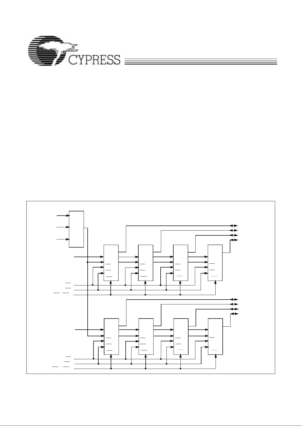
CYM74BP54 is an asynchronous 256-Kbyte cache module
that provides a low-cost, high-performance solution with in-
dustry standard 5V SRAMs and 3.3V level t ranslators for CPU
bus speeds up to 66 MHz. The CYM74BP54 is organized as
32K by 64-bits.
The synchronous modules are available with low-cost synchronous pipelined RAMs or h igher performance sync h ronous
burst RAMs. The synchronous pipelined modules are based
on a 16Kx64 RAM. The CYM74P54 is a 256-KB module while
the CYM74P55 is a 512-KB module. Both are modules without
byte parity.
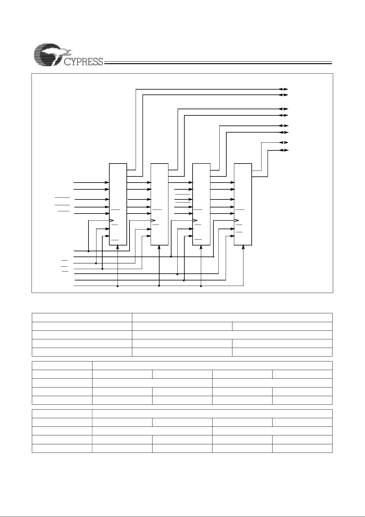
The CYM74SP54 and CYM74SP55 are synchronous burst
cache modules that provide zero wait-state performance at a
bus speed of 66 MHz. The CYM74SP54 is a 256-Kby te cache
module with byte parity. The CYM74SP55 is a 512-Kbyte
cache module with byte parity.
Multiple ground pins and on-board decoupling capacitors ensure high performance with maximum noise immunity.
All components on the cache modules are surface mounted
on a multi-layer epoxy laminate (multifunctional) substrate.
The contact pins are plated with 150 micro-inches of nickel
covered by 10 micro-inches of gold flash.
Intel is a registered trademark of Intel Corporation.
A
Logic Block Diagram -
CYM74BP54
LA17-LA
5
WE
0
WE
1
WE
2
WE
3
AAA
D
DD
D
CE
OE
CE
OE
CE
OE
CE
OE
WE
4
WE
5
WE
6
WE
7
AAAA
D
DD
D
CE
OE
CE
OE
CE
OE
CE
OE
CE
0
OE
0
WE0-WE
3
OE
1
WE4-WE
7
D0-D
7
D8-D
15
D16-D
23
D24-D
31
D32-D
39
D40-D
47
D48-D
55
D56-D
63
32K x 8
32K x 8
32K x 8 32K x 8
32K x 8
32K x 8 32K x 8 32K x
8
A
4–0-A3–0
A
4–1-A3–1
A17-A
7
ADDRESS LATCH
LE
CALE
A
74BP54–1
A
6–0-A5–0
CE
1
CYM74BP54
CYM74P54/55
CYM74SP54/55
PRELIMINARY
2
Block Diagram: 5V to 3.3V Level Conversion (CYM74BP54)
5VSRAM
64BitBusSwitch
5.0Volts
Vcc
(uses7CYBUS3384)
BE
[2:1]
B
D
3.3VcompliantI/O
GND
4.3Vzener
5%tolerance
100ohms
74BP54–2
D
CS
0
OE
CE
0
OE
0
WE7-WE
0
A
A16-A
7
ADV0 ADV
ADSC0 ADSC
ADSP
CLK0
8
BE0-BE
7
CK
A
17
CYM74P55 (A
18
)
CS
1
CS2CS
3
CS
4
V
CC
V
CC
D
CS
0
OE
A
ADV
ADSC
ADSP
CK
CS
1
CS2CS
3
CS
4
V
CC
D
CS
0
OE
A
ADV
ADSC
ADSP
BE0-BE
7
CK
CS
1
CS2CS
3
CS
4
V
CC
D
CS
0
OE
A
ADV
ADSC
ADSP
CK
CS
1
CS2CS
3
CS
4
D63-D
0
GND
GND
GND
GND
CYM74P55ONLY
16Kx64 16Kx64 16Kx64 16Kx64
CYM74P54(GND)
BE0-BE
7
BE0-BE
7
PD2PD1PD
0
CYM74P54
CYM74P55
ADSP0
TBD TBD TBD
TBD TBD TBD
ADV1
ADSC1
ADSP1
CE
1
OE
1
A
6–0-A3–
0
A
6–1-A3–
1
CLK1
74BP54–3
AAAA
Logic Block Diagram - CYM74P54, CYM74P55
CYM74BP54
CYM74P54/55
CYM74SP54/55
PRELIMINARY
3
WE0/1
WE2/3
WE4/5
WE6/7
AAA
D
DD
D
CE
OE
CE
OE
CE
OE
CE
OE
CE
0
OE
0
WE0-WE
7
D0-D
15
D16-D
31
D32-D
47
D48-D
63
A
6–0-A3–0
A
A
18-A7
DP2-DP
3
DP0-DP
1
DP4-DP
5
DP6-DP
7
ADV0
ADV ADV ADV ADV
ADSC0
ADSC ADSC ADSC ADSCADSC ADSC ADSC ADSC
ADSP0
ADSP ADSP ADSP ADSP
CLK0
74BP54–4
(CYM74SP54)32Kx 18
(CYM74SP55)64Kx18
Note:A
18
isnotusedbyCYM74SP54
CLK1
CE
1
OE
1
ADSP1
ADSC1
ADV1
A
6–1-A3–1
Logic Block Diagram - CYM74SP54/CYM74SP55
Selection G uide
Asynchronous Cache Modules
Part Number CYM74BP54-60 CYM74BP54-66
Cache Size (KB) 256
System Clock (MHz) 60 66
RAM Speed tAA=15 ns tAA=12 ns
Synchronous Pipelined Cache Modules
Part Number CYM74P54-60 CYM74P54-66 CYM74P55-60 CYM74P55-66
Cache Size (KB) 256 512
System Clock (MHz) 60 66 60 66
RAM Speed t
CDV
=10.5 ns t
CDV
=8.5 ns t
CDV
=10.5 ns t
CDV
=8.5 ns
Synchornous Burst Cache Modules
Part Number CYM74SP54-60 CYM74SP54-66 CYM74SP55-60 CYM74SP55-66
Cache Size (KB) 256 512
System Clock (MHz) 60 66 60 66
RAM Speed t
CDV
=10.5 ns t
CDV
=8.5 ns t
CDV
=10.5 ns t
CDV
=8.5 ns
 Loading...