

PRELIMINARY
OPTi Viper Chip Set Level II
Cache Module Family
CYM74B550
CYM74P550A
CYM74S550, CYM74S551
Cypress Semiconductor Corporation • 3901 North First Street • San Jose • CA 95134 • 408-943-2600
July 1995 - Revised October 1996
1CYM74S 550,
CYM74S551
Features
• Pin-compatible secondary cache module family
• Asynchronous (CYM74B550), synchronous pipelined
(CYM74P550A), or synchronous burst (CYM74S550,
CYM74S551) modules
• Ideal for Intel P54C/P55C systems with the OPTi Viper
chipset
• Operates at 50, 60, and 66 MHz
• Uses cost-effective CMOS asynchronous SRAMs or
high-performance synchronous SRAMs
• 160-position Burndy DIMM CELP2X80SC3Z48 connector
• 3.3V inputs/ data outputs
Functional Descriptio n
This family of secondary cache modules is designed for Intel
P54C/P55C systems with the OPTi Viper chip set.
CYM74B550 is a low cost a synchronous cache module that
provides 256-Kbytes of cache with industry standard 32Kx8 5
volt SRAMs and 3.3 volt level translators. These modules offer
3-2-2-2 performance at CPU bus speeds up to 66 MHz.
The synchronous modules are available with low cost synchronous pipelined RAMs or high performance synchronous bur st
RAMs.
The CYM74P550A is a high performance synchronous pipelined burst 256 KB module and is based on industry standard
32Kx32 pipelined BSRAM. The CYM74P550A has series
damping resistors on the data lines.
The CYM74S550 and CYM74S551 are high performanc e syn chronous burst cache modules that provide 256-Kbytes and
512-Kbytes of cache respectively. These modules support
3-1-1-1 performance at 66 MHz.
All of these modules include stor age for 8-bits of tag and one
dirty bit. Multiple ground pins and on-board decou pl ing capac itors ensure high performance with maximum noise immunity.
All components on the cache modules are surface mounted on
a multi-layer epoxy laminate (FR-4) substrate. The contact
pins are plated with 100 micro-inches of nickel covered by 10
micro-inches of gold flash.
Intel is a trademark of Intel Corporation. OPTi is a trademark of OPTi, Inc.
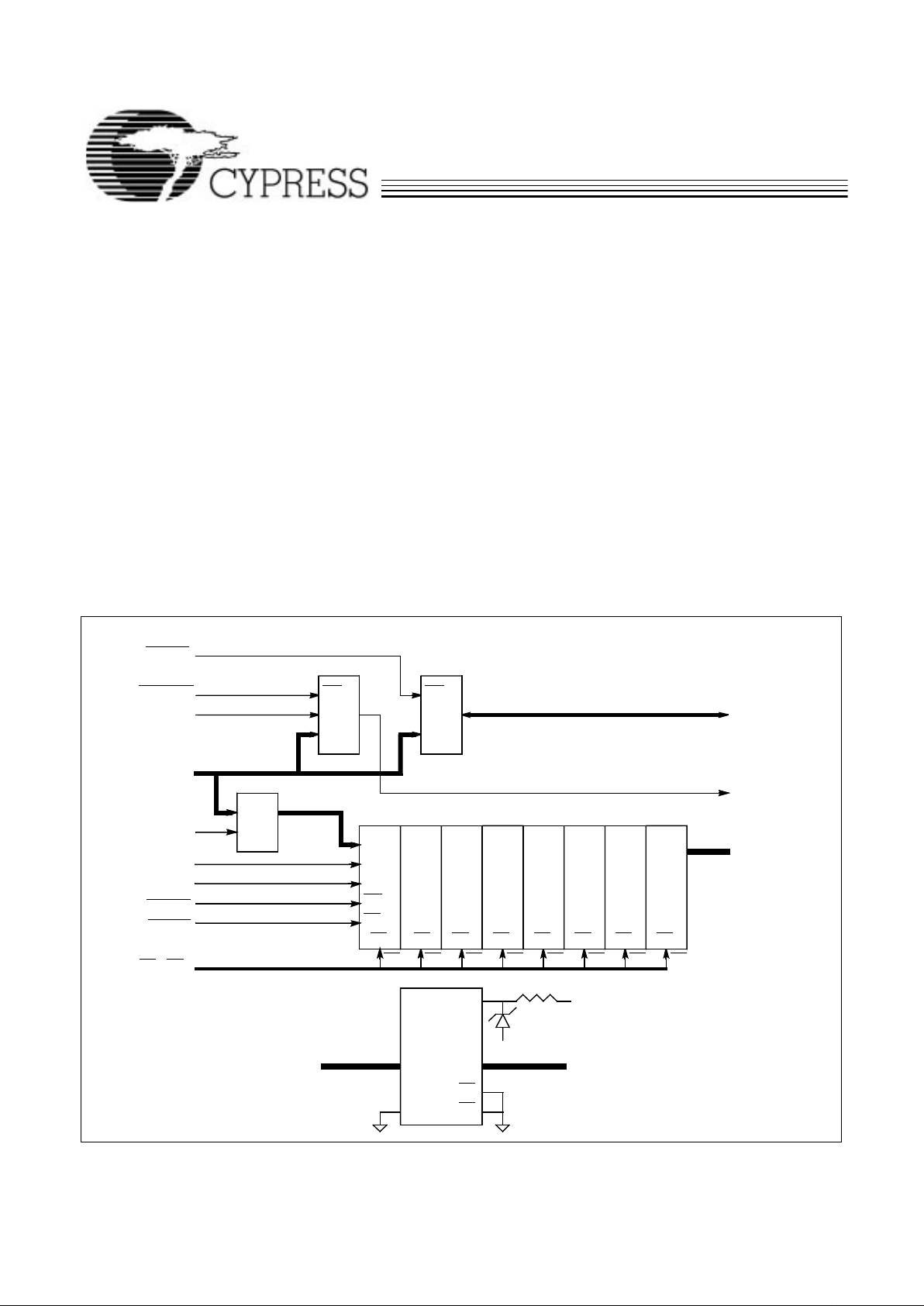
LogicBlockDiagram
-
CYM74B550
CE
D
WE
OE
32Kx 8
A
17–A5
LEHACALE
A
0
CE CE CE CE CE CE CE
A
1
A
14:2
ECA
4
ECAWE
ECDOE
A
17–A5
CS7–CS
0
373C
TAGWE
DIRTYWE
DIRTYI
DIRTYO
TAG
7
–TAG
0
WEWE
16Kx1
8Kx8
D
A
13:0
A
13:0
DQ
CD
63
–CD
0
CS7CS6CS5CS4CS3CS2CS1CS
0
LSB
LA
17
–LA
5
OCA
4
PD3PD2PD1PD
0
GNDGNDNC NCCYM74B550
2X
5V only SRAMs
4.3V zener
5% toler an ce
100 ohms
V
CC5
GND
V
CC
GND
CD
63
–CD
0
D63–D
0
module 3.3V compliant databus
BE
2
BE
1
CYBUS3384
7X
AB
LA
17
–LA
5
A
17–A5
74b550-1
CYM74B550
CYM74P550A
CYM74S550, CYM74S551
PRELIMINARY
2
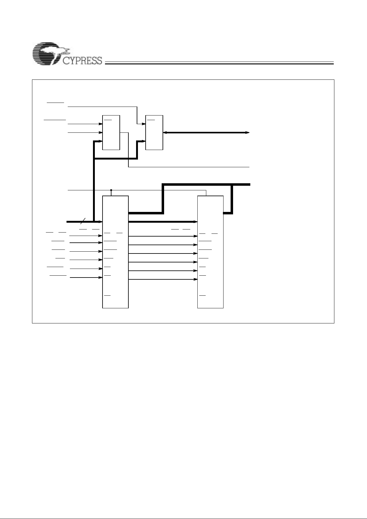
LogicBlock Diagram – CYM74P550A
D
CE
1
OE
SYNCS
0
ECDOE
WE7–WE
0
A
ADV
ADV
ADSC ADSC
ADSP
CLK
15
BE3–BE
0
CK
CE
2
CE
3
D
CE
1
OE
A
ADV
ADSC
ADSP
CK
CE
3
V
SS
32Kx32 32Kx32
BE3–BE
0
TAGWE
DIRTYWE
DIRTYI
DIRTYO
TAG7–TAG
0
WEWE
16Kx1
8Kx8 (CYM74P550A)
D
A
13:0
A
13:0
DQ
PD3PD2PD1PD
0
NCNC NCCYM74P550A GND
ADSP
D63–D
0
D
31–D0
D63–D
32
V
SS
V
CC3
V
CC3
CE
2
WE3–WE
0
WE7–WE
4
A
17–A5
A
17–A3
A
17–A5
74b550-2
CYM74B550
CYM74P550A
CYM74S550, CYM74S551
PRELIMINARY
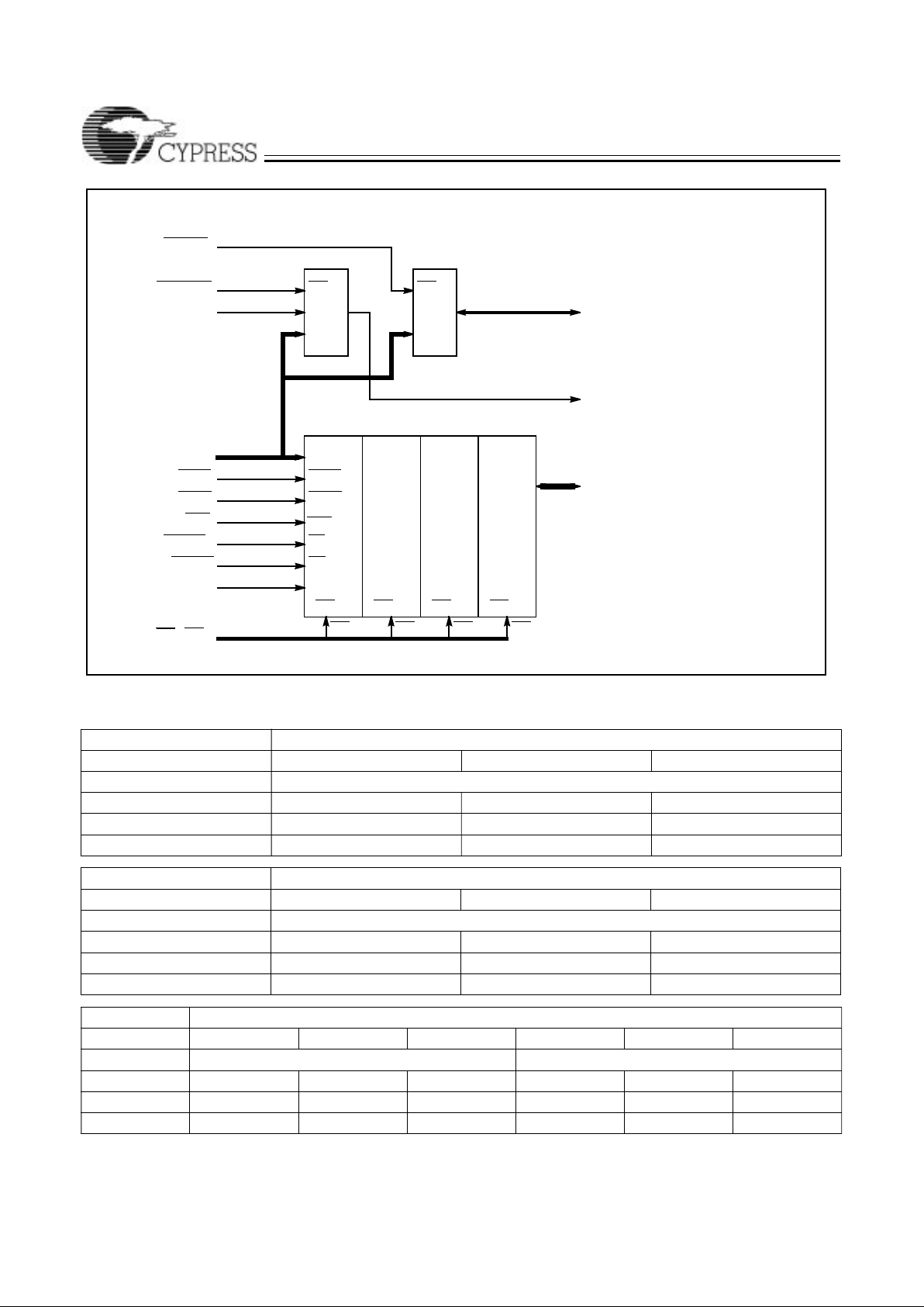
3
WE
1:0
A
15:0
CE
OE
ADV
ADSC
ADSP
Note: A18is not used by CYM74S550
CLK
D
WE
1:0
WE
1:0
WE
1:0
WE
7
–
WE
0
CLK
ECDOE
SYNCS
0
ADV
ADSC
DP Pullup to V
CC3
D63–D
0
WE
1:0
WE
3:2
WE
5:4
WE
7:6
32Kx18(CYM74S550)
64Kx18(CYM74S551)
A
18
–A
3
TAGWE
DIRTYWE
DIRTYI
DIRTYO
TAG7–TAG
0
WEWE
16Kx1
8Kx8 (CYM74S550)
32Kx8 (CYM74S551 )
D
A
13:0
A
13:0
DQ
A
18–A5
A18–A
5
PD3PD2PD1PD
0
NC
NCGND
NCNCNCCYM74S550
CYM74S551
GND
GND
LSBMSB
ADSP
Logic Bl ock Diagram - CYM74S550, CYM74S55 1
74b550-3
Selection G uide
Asynchronous Cache Modules
Part Number 74B550-50 74B550-60 74B550-66
Cache Size 256 KB
System Clock 50 MHz 60 MHz 66 MHz
Data SRAM t
AA
25 ns 15 ns 15 ns
Tag SRAM t
AA
20 ns 15 ns 12 ns
Synchronous Pipelined Cache Modules
Part Number 74P550A-50 74P550A-60 74P550A-66
Cache Size 256 KB
System Clock 50 MHz 60 MHz 66 MHz
Data SRAM t
CO
12 ns 9 ns 9 ns
Tag SRAM t
AA
20 ns 15 ns 12 ns
Synchronous Burst Cache Modules
Part Number 74S550-50 74S550-60 74S550-66 74S551-50 74S551-60 74S551-66
Cache Size 256 KB 512 KB
System Clock 50 MHz 60 MHz 66 MHz 50 MHz 60 MHz 66 MHz
Data SRAM t
CO
12 ns 9 ns 9 ns 12 ns 9 ns 9 ns
Tag SRAM t
AA
20 ns 15 ns 12 ns 20 ns 15 ns 12 ns

CYM74B550
CYM74P550A
CYM74S550, CYM74S551
PRELIMINARY
4
Top View
Pin Configuration
Dual Read-Out SIMM (DIMM)
10
9
5
6
7
8
4
1
2
GND
D
63
GND
D
62
NC (74B550) / V
CC3
(74P550A, 74S55X)
D
58
GND
D
54
V
CC5
D
61
V
CC5
D
59
D
55
D
57
GND
D
56
D
60
3
90
89
85
86
87
88
84
81
82
83
20
19
15
16
17
18
14
11
12
D
52
D
50
D
46
D
44
GND
D40
D
42
GND
D
48
13
30
29
25
26
27
28
24
21
22
D
38
D
36
D
32
D
30
D
26
D
24
GND
D
28
D
34
GND
23
39
35
36
37
38
34
31
32
D
22
D
18
GND
D
14
D
12
D
16
D
20
33
40
41
42
GND
D
10
52
51
47
48
49
50
46
43
44
D
8
D
6
D
4
D
0
GND
D
2
45
57
58
59
60
56
53
54
GND
A
10
A
14
A
12
A
8
55
69
65
66
67
68
64
61
62
A
16
PD
3
CS1(74B550) / WE1(74P550A, 74S55X)
GND
PD
1
63
70
79
75
76
77
78
74
71
72
OCDOE
73
80
D
53
D
51
GND
D
49
D
47
D
45
D
41
D
43
GND
100
99
95
96
97
98
94
91
92
93
D
39
D
37
D
35
GND
D
33
D
31
D
25
GND
D
29
D
27
110
109
105
106
107
108
104
101
102
103
D
23
D
21
V
CC5
D
19
GND
D
15
D
13
D
17
V
CC5
120
119
115
116
117
118
114
111
112
113
GND
D
11
121
122
V
CC5
D
9
V
CC5
D
7
D
5
D
3
D
1
127
128
129
130
126
123
124
125
GND
A
7
A
11
A
13
GND
(74P550A, 74S55X) A
3
/ (74B550) NC
140
139
135
136
137
138
134
131
132
133
A
15
A
17
GND
ECDOE
PD
2
(74P550A, 74S55X) CLK / (74B550) NC
(74P550A, 74S55X) WE
0
/ (74B550) CS
0
150
149
145
146
147
148
144
141
142
143
GND
(74P550A, 74S55X) ADSC
/ (74B550) ECA
4
160
159
155
156
157
158
154
151
152
153
(74P550A, 74S55X) SYNCS
0
/ (74B550) ECAWE
PD
0
TAG
6
TAG
4
TAG
2
V
CC5
TAG
0
DIRTYI
GND
(Reserved A
19
)NC
V
CC5
(74P550A, 74S55X) WE2/ (74B550) CS
2
(74P550A, 74S55X) WE4/ (74B550) CS
4
V
CC5
(74P550A, 74S55X) WE6/ (74B550) CS
6
DIRTYWE
A
5
A
9
V
CC5
OCA4(74B550) / ADV(74P550A, 74S55X)
OCAWE
(74B550) / SYNCS1(74P550A, 74S55X)
CS
3
(74B550) / WE3(74P550A, 74S55X)
CS
5
(74B550) / WE5(74P550A, 74S55X)
CS
7
(74B550) / WE7(74P550A, 74S55X)
HACALE(74B550) / ADSP
(74P550A, 74S55X)
TAGWE
NC (74B550) / A4(74P550A, 74S55X)
A
6
NC (ReservedA20)
GND
DIRTYO
TAG
1
TAG
3
TAG
5
GND
TAG
7
NC (74B550) / V
CC3
(74P550A, 74S55X)
NC (74B550) / V
CC3
(74P550A, 74S55X)
NC (74B550) / V
CC3
(74P550A, 74S55X)
NC (74B550) / V
CC3
(74P550A, 74S55X)
NC (74B550) / V
CC3
(74P550A, 74S55X)
NC (74B550) / V
CC3
(74P550A, 74S55X)
NC (74B550) / V
CC3
(74P550A, 74S55X)
NC (74B550) / V
CC3
(74P550A, 74S55X)
NC (74B550) / V
CC3
(74P550A, 74S55X)
A
18
74b550-4

CYM74B550
CYM74P550A
CYM74S550, CYM74S551
PRELIMINARY
5
Pin Definitions
Common Signals Description
V
CC5
5V Supply
V
CC3
3.3V Supply are CYM74P550A and CYM74S55X only
GND Ground
A18–A
5
Addresses from processor
D63–D
0
64-bit Data bus from processor
ECDOE Even bank output enable input
TAG7–TAG
0
8-bit Ta g RAM bidirectional bus
TAGWE Tag RAM write enable input
DIRTYI 1-bit Dirty RAM input
DIRTYO 1-bit Dirty RAM output
DIRTYWE Dirty RAM write enable input
PD3–PD
0
Presence Detect pins
NC Signal not connected on module.
CYM74B550 Only Signals Description
HACALE Address Latch Enable input to transparent address latches
OCA
4
Address bit A3 in async cache module (CYM74B550)
ECA
4
Address bit A4 in async cache module (CYM74B550)
CS7–CS
0
Data RAM Chip Select inputs
ECAWE Even bank write enable input
CYM74P550A,CYM74S55X
Signals Description
CLK Clock input
A4–A
3
Lower order address bits from processor
ADSC Cache Controller Address Strobe input
ADSP Processor Address Strobe input
ADV Burst Address Advance input
SYNCS
0
Even bank synchronous burst RAM chip select input
SYNCS
1
Odd bank synchronous burst RAM chip select input (not used)
WE7–WE
0
Write enable inputs to Data RAMs
Presence Detect Pins
PD
3
PD
2
PD
1
PD
0
Asynchronous - CYM74B550 NC NC GND GND
Sync Pipelined - CYM74P550A NC NC GND NC
Synch Burst - CYM74S550 NC NC NC GND
Synch Burst - CYM74S551 NC GND NC GND

CYM74B550
CYM74P550A
CYM74S550, CYM74S551
PRELIMINARY
6
Maximum Ratings
(Above which the useful life may be impaired. For user guidelines, not tested.)
Storage Temperature ................................. – 55°C to +125°C
Ambient Temperature
with Power Applied.........................................–0°C to +70°C
3.3V Supply Voltage to Ground Potential....... –0.5V to +4.6V
5V Supply Voltage to Ground Potential..........–0.5V to +7.0V
DC Voltage Applied to Outputs
in High Z State ............................................... –0.5V to +4.6V
DC Input Voltage ............................................–0. 5V to +4.6V
Output Current into Outputs (LOW)............................. 20 mA
Document #: 38-M-00076-A
Operating Range
Range
Ambient
Temperature V
CC5
V
CC3
Commercial
(CYM74B550)
0°C to +70°C 5V ± 5% N/A
Commercial
(CYM74P550A,
CYM74S55X)
0°C to +70°C 5V ± 5% 3.3V
+10%– 5%
Electrical Characteristics Over the Operating Range
Parameter Description Test Condition Min. Max. Unit
V
IH
Input HIGH Voltage 2.2 V
V
IL
Input LOW Voltage CYM74B550 –0.5 0.8 V
V
IL
Input LOW Voltage CYM74P550A, CYM74S55X –0.3 0.8 V
V
OH
Output HIGH Voltage V
CC3
=Min. IOH = -4 mA 2.4 V
V
OL
Output LOW Voltage V
CC3
=Min. IOL = 8 mA 0.4 V
I
CC (74B55 0)
Operating Supply Current V
CC5
=Max., I
OUT
=0 mA, f=f
MAX
1650 mA
I
CC (74P55 0 A )
Operating Supply Current V
CC5
=Max.,V
CC3
=Max., I
OUT
=0 mA,
f=f
MAX
900 mA
I
CC (74S55 0)
Operating Supply Current V
CC5
=Max., V
CC3
=Max., I
OUT
=0 mA,
f=f
MAX
1500 mA
I
CC (74S55 1)
Operating Supply Current V
CC5
=Max., V
CC3
=Max., I
OUT
=0 mA,
f=f
MAX
1500 mA
Ordering Info rma tio n
Speed
(MHz) Ordering Code
Package
Name Package Type Description
Operating
Range
50 CYM74B550PM-50C PM35 160-Pin Dual-Readout SIMM Async 256 KB Commercial
CYM74P550APM-50C PM42 Sync Pipelined 256 KB
CYM74S550PM-50C PM33 Sy nc Burst 256 KB
CYM74S551PM-50C Sync Burst 512 KB
60 CYM74B550PM-60C PM35 160-Pin Dual-Readout SIMM Async 256 KB Commercial
CYM74P550APM-60C PM42 Sync Pipelined 256 KB
CYM74S550PM-60C PM33 Sy nc Burst 256 KB
CYM74S551PM-60C Sync Burst 512 KB
66 CYM74B550PM-66C PM35 160-Pin Dual-Readout SIMM Async 256 KB Commercial
CYM74P550APM-66C PM42 Sync Pipelined 256 KB
CYM74S550PM-66C PM33 Sy nc Burst 256 KB
CYM74S551PM-66C PM33 Sy nc Burst 512 KB

CYM74B550
CYM74P550A
CYM74S550, CYM74S551
PRELIMINARY
7
Package Diagrams
160-Pin Dual Readout SI MM (PM35)
160-Pin Dual Readout SIMM (PM33)

CYM74B550
CYM74P550A
CYM74S550, CYM74S551
PRELIMINARY
© Cypress Semiconductor Corporation, 1996. The information contained herein is subject to change without notice. Cypress Semiconductor Corporation assumes no responsi bility for the us e
of any circuitry othe r than circui try embodi ed in a Cypress Semi conductor p roduct. Nor does it convey or imply any licens e under patent or other rights. Cypress Semi conductor does not authori ze
its products for use as critical components in life-support systems where a malfunction or failure may reasonably be expected to result in significant injury to the user. The inclusion of Cypress
Semiconductor products in life-support systems application implies that the manufacturer assumes all risk of such use and in doing so indemnifies Cypress Semiconductor against all charges.
Package Diagrams (continued)
160-Pin Dual Readout SIMM (PM42)
 Loading...