

Cypress Semiconductor CYM1841APZ-55C, CYM1841APZ-45C, CYM1841APZ-35C, CYM1841APZ-30C, CYM1841APZ-25C Datasheet
...
256K x 32 Static RAM Module
CYM1841A
CYM1841B
CYM1841C
Cypress Semiconductor Corporation
• 3901 North First Street • San Jose • CA 95134 • 408-943-2600
June 13, 2000
Features
• High-density 8-megabit SRAM module
• 32-bit standard footprint supports densities from 16K
x 32 through 1M x 32
• High-speed CMOS SRAMs
—Access time of 12 ns
• Low active power
—5.3W (max.) at 25 ns
• SMD technology
• TTL-compatibl e inputs and outputs
• Low pr o file
—Max. height of 0.58 in.
• Av ailable in ZIP, SIMM, and angled SIMM footprint
• 72-pin SIMM versio n compa ti ble with 1M x 32
(CYM1851)
Functional Description
The CYM1841A/B/C are high-performance 8-megabit static
RAM modules organiz ed as 256K words by 32 bits . This m odule is constructed from eight 256K x 4 SRAMs (1841A/C) or
256K x 16 SRAMs (1841B) in SOJ packages mounted on an
epoxy laminate board with pins. Four chip selects (CS
1
, CS2,
CS
3
, CS4) are used to independently enable the four bytes.
Reading or writing c an be executed on individual bytes or any
combination of mul ti p le bytes through proper use of selec ts.
Writing to each byte is accomplished when t he appropriate
Chip Select (CS
) and Write Enab le (WE) input s are both LOW.
Data on the I nput/Output pins (I/ O) is written into the memory
location specifi ed on the address pins (A
0
through A17).
Reading the device is accomplishe d by taking the Chip Sel ect
(CS
) LOW while Write Enable (WE) remains HIGH. Under
these conditions, t he contents of the memory location specified on the address pins will appear on the data Input/Output
pins (I/O).
The data input/output pins stay at the high-impedance state
when write enable is LOW or the approp riat e chip selects are
HIGH.
Two pins (PD
0
and PD1) are used to i dentify module memory
density in applications where alternate versions of the JEDEC-standard modules can be interchanged.
The CYM1841A, CYM1841B, and CYM1841C are 100% pin,
package, and electrically identical. The CYM1841A utilizes
corner power and ground SRAMs, the CYM1841B utilizes
256K x 16 SRAMs, the CYM1841C utilizes center power and
ground SRAMs.
A 72-pin SIMM is offered for compatibility with the 1M x 32
CYM1851. This ver sion is sock et upg radabl e to the CYM1851.
Both the 64-pin and 72-pin SIMM modules are available with
either tin-lead or 10 micro-inches of gold flash on t he edge
contacts.
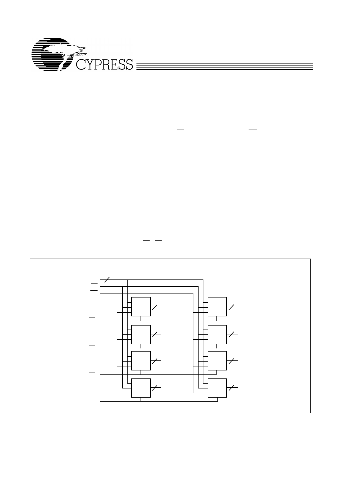
LogicBlockDiagram
1841A–1
A0–A
17
OE
I/O0–I/O
3
CS
3
I/O4–I/O
7
CS
1
18
44
44
44
44
CS
2
CS
4
I/O8–I/O
11
I/O16–I/O
19
I/O24–I/O
27
I/O12–I/O
15
I/O20–I/O
23
I/O28–I/O
31
PD0–GND
PD
1
–GND
PD
2
– OPEN (72-pin only)
PD
3
– OPEN (72-pin only)
WE
256K x 4
SRAM
256K x 4
SRAM
256K x 4
SRAM
256K x 4
SRAM
256K x 4
SRAM
256K x 4
SRAM
256K x 4
SRAM
256K x 4
SRAM

CYM1841A
CYM1841B
CYM1841C
2
LogicBlockDiagram (1841B)
1841A–1
A0–A
17
OE
CS
3
I/O16–I/O
23
CS
1
18
8
8
8
8
CS
2
CS
4
I/O24–I/O
31
I/O0–I/O
7
I/O8–I/O
15
PD0– GND
PD
1
– GND
PD
2
– OPEN (72-pin only)
PD
3
– OPEN (72-pin only)
WE
256K x 16
SRAM
256K x 16
SRAM
Selection Guid e
1841C-12 1841B/C-15 1841A/B/C-20 1841A/B/C-25 1841A/B/C-35 1841A/B/C-45
Maximum Access Time (ns) 12 15 20 25 35 45
Maximum Operat ing
Current (mA)
1600 1600 1120 960 960 960
Maximum Standby
Current (mA)
480 480 480 480 480 480
Shaded areas contain preliminary information.

CYM1841A
CYM1841B
CYM1841C
3
Pin Configurations
CS
WE
1841A–2
SIMM
Top View
NC
A
4
PD
3
PD
2
PD
0
GND
I/O
0
PD
1
I/O
1
I/O
8
I/O
2
I/O
9
I/O
3
V
CC
A
7
I/O
11
I/O
10
A
0
I/O
6
GND
NC
A
15
2
4
6
8
10
12
14
16
18
20
22
24
26
28
30
32
34
36
38
40
42
44
46
48
50
52
54
56
58
60
62
64
1
3
5
7
9
11
13
15
17
19
21
23
25
27
29
31
33
35
37
39
41
43
45
47
49
51
53
55
57
59
61
63
I/O
7
WE
A
8
A
9
I/O
4
I/O
5
A
14
CS
1
CS
3
A
16
GND
I/O
16
I/O
17
A
12
A
13
I/O
20
I/O
21
I/O
22
I/O
14
I/O
15
A
1
A
2
I/O
12
I/O
13
2
I/O
18
I/O
19
A
10
A
11
CS
4
A
17
OE
I/O
24
I/O
25
V
CC
A
6
I/O
28
I/O
29
I/O
26
I/O
27
A
3
A
5
66
68
70
65
67
69
I/O
23
GND
A
19
I/O
30
I/O
31
A
18
72
71
NC
NC
1841A–3
ZIP/SIMM
Top View
PD
0
V
CC
I/O
0
PD
1
I/O
1
I/O
8
I/O
2
I/O
9
I/O
3
I/O
10
V
CC
I/O
11
A
7
A
8
A
9
A
1
A
0
A
2
CS
2
GND
CS
4
2
4
6
8
10
12
14
16
18
20
22
24
26
28
30
32
34
36
38
40
42
44
46
48
50
52
54
56
58
60
62
64
1
3
5
7
9
11
13
15
17
19
21
23
25
27
29
31
33
35
37
39
41
43
45
47
49
51
53
55
57
59
61
63
A
14
CS
1
I/O
4
I/O
5
I/O
6
7
CS
3
A
16
GND
I/O
16
I/O
17
I/O
18
I/O
19
I/O
20
I/O
21
I/O
22
I/O
23
GND
GND
A
I/O
12
I/O
13
I/O
14
I/O
15
A
17
A
10
A
11
A
12
A
13
OE
I/O
24
I/O
25
I/O
26
I/O
27
I/O
28
I/O
29
I/O
30
I/O
31
A
3
A
4
A
5
A
6
64-Pin
72-Pin
15
I/O

CYM1841A
CYM1841B
CYM1841C
4
Maximum Ratings
(Above which the useful life may be impaired. For use r guidelines, not tested.)
Storage Temperature
..................................... –
55°C to +125°C
Ambient Temperature wi th
Po wer Applied
.................................................... –
10°C to +8 5 °C
Supply Voltage to Ground Potential
..................–
0.5V to +7.0V
DC Voltage Applied to Outputs
in High Z State
..................................................... –
0.5V to +7 . 0V
DC Input Voltage
................................................. –
0.5V to +7 . 0V
Operating Range
Range
Ambient
Temperature
V
CC
Commercial 0°C to +70°C 5V ± 10%
Electrical Characteristics
Over the Operating Range
Parame-
ter Description Test Conditions
1841C
-
12
1841B/C
-
15
1841A/B/C
-20
1841A/B/C
-25, 35, 45
UnitMin. Max. Min. Max. Min. Max.
V
OH
Output HIGH
Voltage
VCC = Min., IOH = –4.0 mA 2.4 2.4 2.4 V
V
OL
Output LO W
Voltage
VCC = Min., IOL = 8.0 mA 0.4 0.4 0.4 V
V
IH
Input HIGH
Voltage
2.2 V
CC
2.2 V
CC
2.2 V
CC
V
V
IL
Input LOW
Voltage
–0.5 0.8 –0.5 0.8 –0.5 0.8 V
I
IX
Input Leakage Current
GND < VI < V
CC
–16 +16 –16 +16 –16 +16 mA
I
OZ
Output Leakage Current
GND < VO < VCC,
Output Disabled
–10 +10 –10 +10 –10 +10 mA
I
CC
VCC Operating
Supply Current
VCC = Max., I
OUT
= 0 mA,
CS
< V
IL
1600 1120 960 mA
I
SB1
Auto matic CS
Power-Down
Current
[1]
Max. VCC, CS > VIH,
Min. Duty Cycle = 100%
480 480 480 mA
I
SB2
Auto matic CS
Power-Down
Current
[1]
Max. VCC, CS > VCC -
0.2V,
V
IN
> VCC – 0.2V,
or V
IN
< 0.2V
240
200 200 mA
Capacitance
[2]
Parameter Descri ption Test Conditions Max. Unit
C
IN
Input Capacitance
[3]
T
A
= 25°C, f = 1 MH z,
V
CC
= 5.0V
70/20 pF
C
OUT
Output Capacitanc e 20 pF
Notes:
1. A pull-up resistor to V
CC
on the CS input is required to keep the device deselected during VCC power-up, otherwise ISB will exceed values given.
2. Tested on a sample basis.
3. 20 pF on CS
, 70 pF all others.

CYM1841A
CYM1841B
CYM1841C
5
AC Test Loads and Waveforms
1841A–4
1841A–5
90%
10%
3.0V
GND
90%
10%
ALL INPUT PULSES
5V
OUTPUT
30 pF
INCLUDING
JIG AND
SCOPE
5V
OUTPUT
5 pF
INCLUDING
JIG AND
SCOPE
(a) (b)
<5ns <5ns
OUTPUT
R1481
Ω
R1481
Ω
R2
255
Ω
R2
255
Ω
167
Ω
Equivalent to: THÉ VENIN EQUIVALENT
1.73V
 Loading...