

Datasheet CYM1836PZ-25C, CYM1836PZ-20C, CYM1836PZ-15C, CYM1836PM-45C, CYM1836PM-35C Datasheet (Cypress Semiconductor)
...
CYM1836
128K x 32 Static RAM Module
Features
constructed from four 128K x 8 SRAMs in SOJ packages
mounted on an epoxy laminate board with pins. Four chip se-
• High-density 4-megabit SRAM module
• 32-bit standard footprint supports densities from 16K
x 32 through 1M x 32
• High-speed CMOS SRAMs
—Access time of 15 ns
• Low active power
—2.6W (max.) at 20 ns
• SMD technology
• TTL-compatible inputs and outputs
• Low profile
—Max. height of 0.57 in.
• Small PCB footprint
—0.78 sq. in.
• Av ailable in SIMM, ZIP f ormat. SIMM suitable for vertical
or angled sockets.
Functional Description
The CYM1836 is a high-performance 4-megabit static RAM
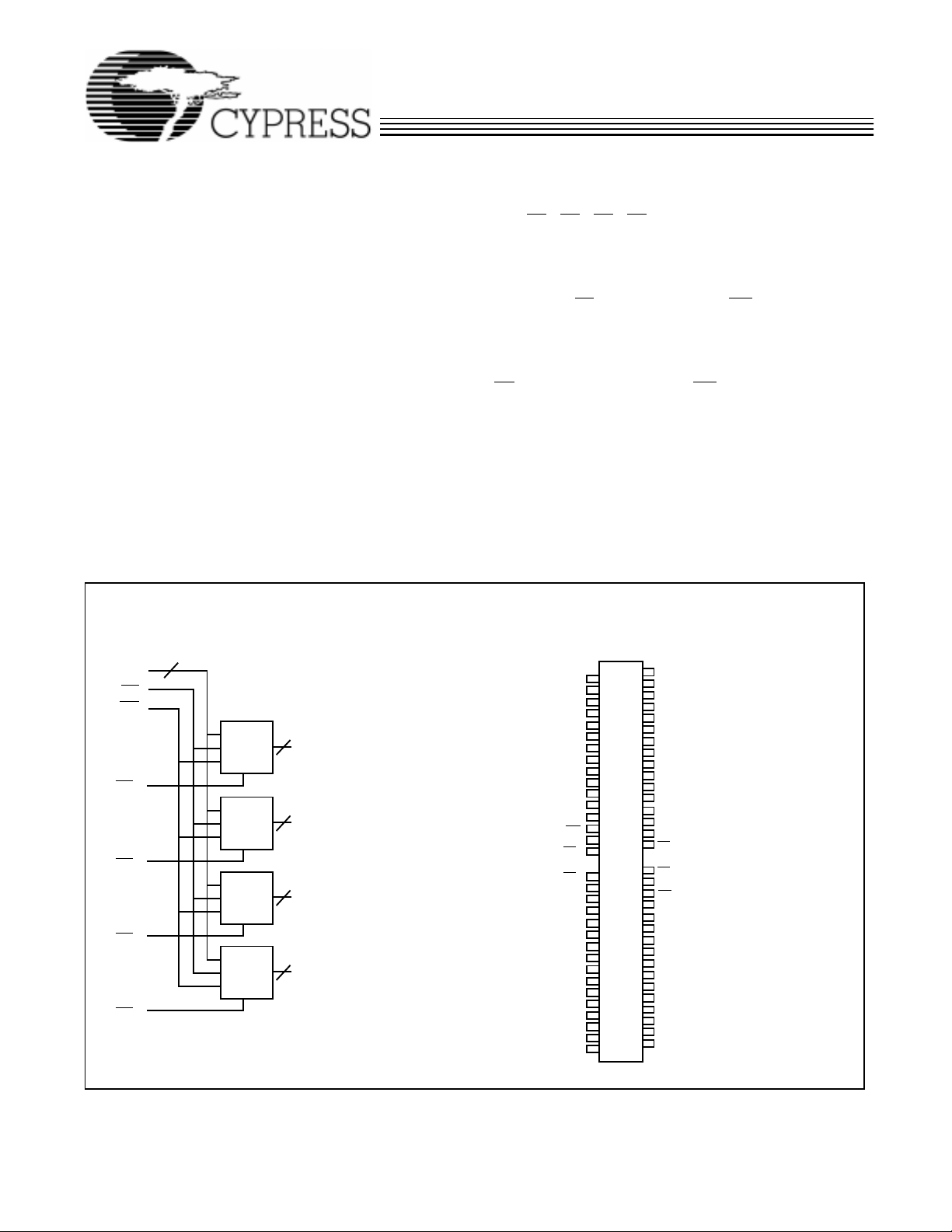
lects (CS
the four bytes. Reading or writing can be executed on individual bytes or any combination of multiple bytes through proper
use of selects.
Writing to each byte is accomplished when the appropriate
Chip Select (CS
LOW. Data on the input/ outp ut pi ns (I/O ) is wri tte n into the
memory location specifi ed on the ad dre ss pins (A
A
Reading the device is accomplished by taking the Chip Select
(CS
these conditions, the contents of the memory location
specified on the address pins will appear on the data input/output pins (I/O).
The data input/output pins stay at the high-impedance state
when write enable is LOW or the appropriate chip selects are
HIGH.
Two pins (PD
ory density in applications where alternate versions of the
JEDEC-standa rd mod ule s can be inte rcha nged .
module organized as 128K words by 32 bits. This module is
Logic Block Diagram Pin Configuration
−
PD
OPEN
0
−
PD
OPEN
−
A
A
0
16
OE
WE
CS
1
CS
2
CS
3
CS
4
1
17
128K x 8
SRAM
128K x 8
SRAM
128K x 8
SRAM
128K x 8
SRAM
I/O
4
I/O
4
I/O
4
I/O
4
1836–1
−
I/O
0
7
−
I/O
8
15
−
I/O
16
23
−
I/O
24
31
, CS2, CS3, CS4) are used to independently enable
1
) and Write Enable (WE) inputs are both
through
16
).
0
) LOW while Write Enable (WE) remains HIGH. Under
and PD1) are used to identify module mem-
0
ZIP/SIMM
Top View
GND
1
2
4
6
8
10
12
14
16
18
20
22
24
26
28
30
32
34
36
38
40
42
44
46
48
50
52
54
56
58
60
62
64
11
13
15
17
19
21
23
25
27
29
31
33
35
37
39
41
43
45
47
49
51
53
55
57
59
61
63
3
5
7
9
PD
I/O
I/O
I/O
I/O
A
A
A
I/O
I/O
I/O
I/O
GND
A
CS
CS
NC
OE
I/O
I/O
I/O
I/O
A
A
A
V
A
I/O
I/O
I/O
I/O
1836–2
1
8
9
10
11
0
1
2
12
13
14
15
15
2
4
24
25
26
27
3
4
5
CC
6
28
29
30
31
I/O
I/O
I/O
I/O
I/O
I/O
I/O
I/O
PD
I/O
I/O
I/O
I/O
V
CC
A
A
A
I/O
I/O
I/O
I/O
WE
A
CS
CS
A
GND
16
17
18
19
A
A
A
A
20
21
22
23
GND
0
0
1
2
3
7
8
9
4
5
6
7
14
1
3
16
10
11
12
13
Cypress Semiconductor Corporation
• 3901 North First Street • San Jose • CA 95134 • 408-943-2600
February 15, 1999
CYM1836
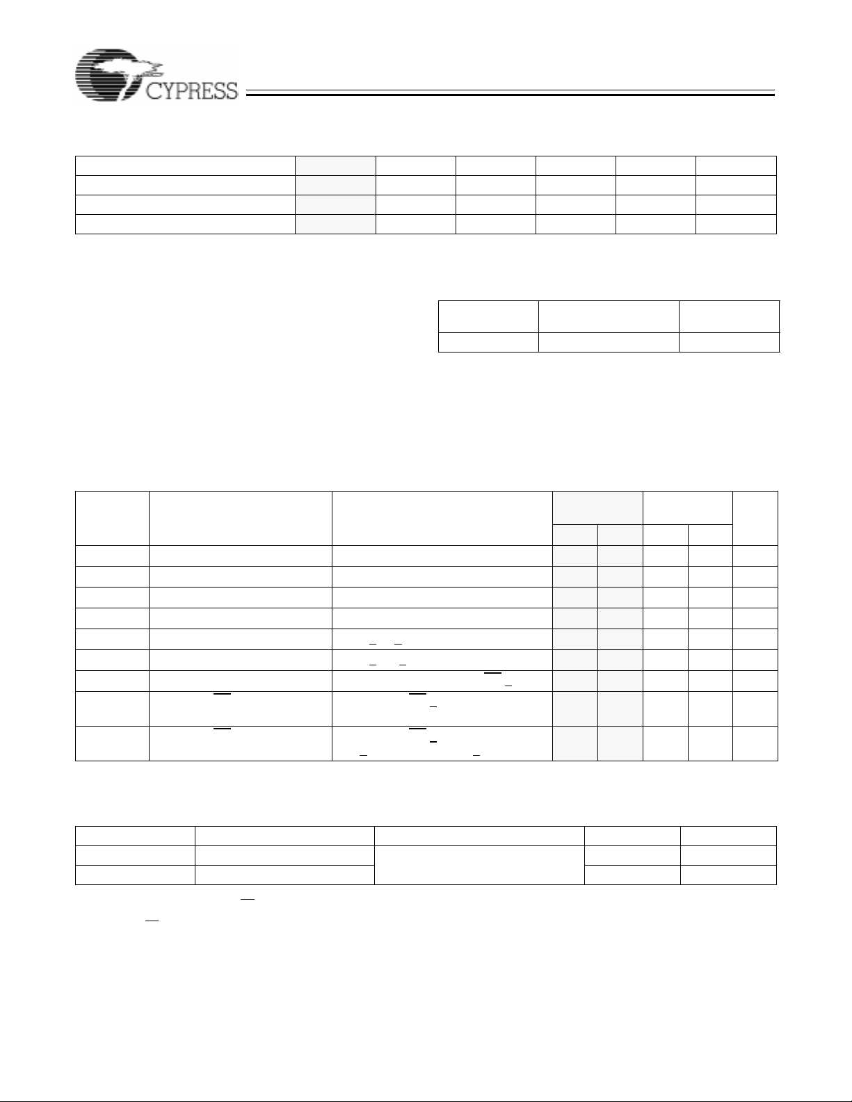
Selection Guide
1836–15 1836–20 1836–25 1836–30 1836–35 1836–45
Maximum Access Time (ns) 15 20 25 30 35 45
Maximum Operating Current (mA) 760 480 480 480 480 480
Maximum Standby Current (mA) 180 100 100 100 100 100
Shaded area contains preliminary information.
Maximum Ratings
Operating Range
(Above which the useful life may be impaired. For user guidelines, not tested.)
Storage Temperature .................................–55°C to +125°C
Commercial 0°C to +70°C 5V ± 10%
Ambient Temperature with
Po wer Applied...............................................–10°C to +85°C
Supply Voltage to Ground Potential...............–0.5V to +7.0V
DC Voltage Applied to Outputs
in High Z State...............................................–0.5V to +7.0V
DC Input Voltage............................................–0.5V to +7.0V
Electrical Characteristics
Over the Operating Range
Parameter Description Test Conditions
V
OH
V
OL
V
IH
V
IL
I
IX
I
OZ
I
CC
I
SB1
I
SB2
Shaded area contains preliminary information.
Output HIGH Voltage VCC = Min., IOH = –4.0 mA 2.4 2.4 V
Output LOW Voltage VCC = Min., IOL = 8.0 mA 0.4 0.4 V
Input HIGH Voltage 2.2 V
Input LOW Voltage –0.5 0.8 –0.5 0.8 V
Input Load Current GND < VI < V
CC
Output Leakage Current GND < VO < VCC, Output Disabled –20 +20 –20 +20 µA
VCC Operating Supply Current VCC = Max., I
Automatic CS Power-Down
[1]
Current
Automatic CS Power-Down
[1]
Current
VCC = Max., CS > VIH,
Min. Duty Cycle = 100%
VCC = Max., CS > VCC – 0.2V,
> VCC – 0.2V or VIN < 0.2V
V
IN
= 0 mA, CS < V
OUT
Range
Ambient
Temperature V
1836–20, 25,
1836–15
CC
30, 35, 45
2.2 V
–20 +20 –20 +20 µA
IL
760 480 mA
180 100 mA
60 28 mA
CC
CC
UnitMin. Max. Min. Max.
V
Capacitance
[2]
Parameter Description Test Conditions Max. Unit
C
IN
C
OUT
Notes:
1. A pull-up resistor to V
2. Tested on a sample basis.
3. 20 pF on CS
CC
, 40 pF all others.
Input Capacitance
Output Capacitance 15 pF
on the CS input is required to keep the device deselected during VCC power-up, otherwise ISB will exceed values given.
[3]
TA = 25°C, f = 1 MHz,
= 5.0V
V
CC
40/20 pF
2
AC Test Loads and Waveforms
CYM1836
Ω
5V
OUTPUT
INCLUDING
JIG AND
SCOPE
Equivalent to: THÉ VENIN EQUIVALENT
OUTPUT
R1 481
OUTPUT
R2
Ω
167
Ω
255
INCLUDING
JIG AND
SCOPE
1.73V
30 pF
(a) (b)
5V
5 pF
R1 481
Ω
R2
255
1836–3
3.0V
GND
Ω
< 5ns < 5 ns
ALL INPUT PULSES
90%
10%
90%
10%
1836–4
3

CYM1836
Switching Characteristics
Parameter Description
READ CYCLE
t
RC
t
AA
t
OHA
t
ACS
t
DOE
t
LZOE
t
HZOE
t
LZCS
t
HZCS
WRITE CYCLE
t
WC
t
SCS
t
AW
t
HA
t
SA
t
PWE
t
SD
t
HD
t
LZWE
Read Cycle Time 15 20 25 30 35 45 ns
Address to Data
Valid
Output Hold from
Address Change
CS LOW to Data
Valid
OE LOW to Data
Valid
OE LOW to
Low Z
OE HIGH to High
Z
CS LOW to
[5]
Low Z
CS HIGH to High
[5, 6]
Z
[7]
Write Cycle Time 15 20 25 30 35 45 ns
CS LOW to Write
End
Address Set-Up
to Write End
Address Hold
from Write End
Address Set-Up
to Write Start
WE Pulse Width 12 15 15 18 20 25 ns
Data Set-Up to
Write End
Data Hold from
Write End
WE HIGH to Low Z3 3 3 3 3 3 ns
Over the Operating Range
[4]
1836–15 1836–20 1836–25 1836–30 1836–35 1836– 45
15 20 25 30 35 45 ns
3 3 3 3 3 3 ns
15 20 25 30 35 45 ns
7 8 8 10 12 15 ns
0 0 0 0 0 0 ns
7 8 10 11 12 15 ns
3 3 3 3 3 3 ns
7 10 10 13 15 18 ns
12 15 15 18 20 25 ns
12 15 15 18 20 25 ns
0 0 0 0 0 0 ns
0 0 0 0 0 0 ns
7 10 10 13 15 20 ns
0 0 0 0 0 0 ns
UnitMin. Max. Min. Max. Min. Max. Min. Max. Min. Max. Min. Max.
t
HZWE
Shaded area contains preliminary information.
Notes:
4. Test conditions assume signal transition times of 5 ns or less, timing reference levels of 1.5V , input pulse levels of 0 to 3.0V, and output loading of the specified
I
OL/IOH
5. At any given temperature and voltage condition, t
6. t
HZCS
7. The internal write time of the memory is defined by the overlap of CS
terminate a write by going HIGH. The data input set-up and hold timing should be referenced to the rising edge of the signal that terminates the write.
WE LOW to High
[6]
Z
and 30-pF load capacitance.
and t
are specified with CL = 5 pF as in part (b) of AC Test Loads and Waveforms. Transition is measured ±500 mV from steady-state voltage.
HZWE
0 6 0 8 0 10 0 15 0 15 0 18 ns
HZCS
is less than t
for any given device. These parameters are guaranteed by design and not 100% tested.
LZCS
LOW and WE LOW. Both signals must be LOW to initiate a write and either signal can
4

Switching Waveforms
CYM1836
Read Cycle No.1
ADDRESS
DATA OUT
Read Cycle No. 2
CS
OE
DATA OUT
[8, 9]
t
RC
t
t
OHA
AA
PREVIOUS DATA VALID DATA VALID
[8, 10]
t
RC
t
ACS
t
DOE
t
LZOE
HIGH IMPEDANCE
t
LZCS
DATA VALID
t
HZOE
t
HZCS
1836–5
HIGH
IMPEDANCE
1836–6
Write Cycle No.1 (WE Controlled )
[7]
ADDRESS
CS
t
SA
WE
DATA IN
DATA
OUT
Notes:
8. WE
is HIGH for read cycle.
9. Device is continuously selected, CS = VIL and OE= VIL.
10. Address valid prior to or coincident with CS
DATA UNDEFINED
transition LOW.
t
SCS
t
AW
t
WC
DATA VALID
t
HZWE
t
PWE
t
HA
t
SD
t
HD
t
LZWE
HIGH IMPEDANCE
1836–7
5

CYM1836
Switching Waveforms
(continued)
Write Cycle No.2 (CS Controlled)
ADDRESS
CS
WE
DATA IN
OUT
DATA
Note:
11. If CS
goes HIGH simultaneously with WE HIGH, the output remains in a high-impedance state.
[7, 11]
t
SA
DATA UNDE FINED
t
AW
t
WC
t
SCS
t
PWE
t
SD
DATA VALID
t
HZWE
t
HA
t
HD
HIGH IMPEDANCE
1836–8
Truth Tab le
CS
N
H X X High Z Deselect/Power-Down
L H L Data Out Read
L L X Data In Write
L H H High Z Deselect
WE OE Input/Outputs Mode
6

CYM1836
Ordering Information
Speed
(ns) Ordering Code
[12]
Package
Name Package Type
15 CYM1836PM–15C PM03 64-Pin SIMM Module Commercial
CYM1836PZ–15C PZ08 64-Pin ZIP Module
CYM1836PY–15C PM08 64-Pin Gold SIMM Module
CYM1836P8–15C PM04 72-Pin Gold SIMM Module
20 CYM1836PM–20C PM03 64-Pin SIMM Module Commercial
CYM1836PZ–20C PZ08 64-Pin ZIP Module
CYM1836PY–20C PM08 64-Pin Gold SIMM Module
CYM1836P8–20C PM04 72-Pin Gold SIMM Module
25 CYM1836PM–25C PM03 64-Pin SIMM Module Commercial
CYM1836PZ–25C PZ08 64-Pin ZIP Module
CYM1836PY–25C PM08 64-Pin Gold SIMM Module
CYM1836P8–25C PM04 72-Pin Gold SIMM Module
30 CYM1836PM–30C PM03 64-Pin SIMM Module Commercial
CYM1836PZ–30C PZ08 64-Pin ZIP Module
CYM1836PY–30C PM03 64-Pin Gold SIMM Module
CYM1836P8–30C PM04 72-Pin Gold SIMM Module
35 CYM1836PM–35C PM03 64-Pin SIMM Module Commercial
CYM1836PZ–35C PZ08 64-Pin ZIP Module
CYM1836PY–35C PM03 64-Pin Gold SIMM Module
CYM1836P8–35C PM04 72-Pin Gold SIMM Module
45 CYM1836PM–45C PM03 64-Pin SIMM Module Commercial
CYM1836PZ–45C PZ08 64-Pin ZIP Module
CYM1836PY–45C PM03 64-Pin Gold SIMM Module
CYM1836P8–45C PM04 72-Pin Gold SIMM Module
Shaded area contains preliminary information.
Note:
12. 64-pin SIMM suitable for use in angled SIMM applications.
Operating
Range
Document #: 38–M–00050–D
Package Diagrams
64-Pin SIMM Module PM03
3.855 MAX.
124/.126 DIA.
2 PLCS
128KX8 128KX8 128KX8 128KX8
.397/.403
.245/.255
PIN 1
.075/.085 .249/.251
3.580/3.588
.061/.063 R
7
. 200 MAX.
.595 MAX.
.135 REF.

CYM1836
Package Diagrams
(continued)
72-Pin Plastic SIMM Module PM04
64-Pin ZIPModule PZ08
© Cypress Semiconductor Corporation, 1999. The information contained herein is subject to change without notice. Cypress Semiconductor Corporation assumes no responsibility for the use
of any circuitry other than circui try embodied in a Cypress S emiconductor p roduct. Nor does it conv ey or imply an y license under pa tent or other rights. Cypress S emiconductor doe s not authorize
its products for use as critical components in life-support systems where a malfunction or failure may reasonably be expected to result in significant injury to the user. The inclusion of Cypress
Semiconductor products in life-support systems application implies that the manufacturer assumes all risk of such use and in doing so indemnifies Cypress Semiconductor against all charges.
 Loading...