


5.2 BLE Module Board
No Load
al Pins
PCA: 121-60159-01
P6.0
P6.1
/XRES
P4.0
P4.1
P5.0
P5.1
XTAL24I
XTAL24O
P2.6
P2.7
P3.0
P3.1
P3.2
P3.3
P3.4
P3.5
P3.6
P3.7
P1.6
P1.5
P1.4
P1.3
P1.2
P1.1
P2.4
P2.3
P2.2
P2.1
P2.0
P1.7
P2.5
P0.5
P0.3
P0.1
P1.0
P1.2
P0.0
P0.1
P0.2
P0.3
P0.4
P0.5
P0.6
P0.7
P1.0
VCCD
VDDD
VDDR
VDDA VREF
VDDA
VDDD
C13
1.2 pF
ER 10x2
12
14
16
18
20
L1
6.8nH
CY8C4247LQI-BL483
U1
VDDD
1
XTAL32O/P6.0
2
XTAL32I/P6.1
3
XRES
4
P4.0
5
P4.1
6
P5.0
7
P5.1
8
VSSD
9
VDDR
10
GANT1
11
ANT
12
GANT2
13
VDDR
14
P2.5
42
P2.4
41
P2.3
40
P2.2
39
P2.1
38
P2.0
37
VDDA
36
P1.7
35
P1.6
34
P1.5
33
P1.4
32
P1.3
31
P1.2
30
P1.1
29
EPAD
57
VCCD
56
VSSA
55
P3.754P3.653P3.552P3.451P3.350P3.249P3.148P3.0
47
VDDA
46
VREF
45
P2.744P2.6
43
VDDR15XTAL24I16XTAL24O17VDDR
18
P1.0
28
P0.019P0.120P0.221P0.322VDDD23P0.424P0.525P0.626P0.7
27
J4
50 Ohm Wiggle Antenna
11
22
C14
1.5 pF
5.2.1 PSoC 4 BLE or PRoC BLE
The PRoC BLE or PSoC 4 BLE is the main component on the BLE Module. It provides the RF
interface and analog and digital capability. The PRoC BLE or PSoC 4 BLE pins are mapped to the
Bluetooth module headers (see Figure 5-20). For more information, refer to the BLE web page.
Figure 5-20. Schematics and Board Highlight of Bluetooth Module Headers for BLE Pins
Hardware
CY8CKIT-042-BLE Bluetooth® Low Energy (BLE) Pioneer Kit Guide, Doc. # 001-93731 Rev. *A 106

5.2.2 Bluetooth Module Headers (20-Pin and 24-Pin Headers)
Analog Pins
Digital Pins
P3.7P3.6
P3.5P3.4
P3.3P3.2
P3.1P3.0
P5.1P4.0
P5.0P4.1
P2.7P2.6
P2.5P2.4
P2.3P2.2
P2.1P2.0
P1.7
P1.5
P1.3
P0.5
P0.3
P0.1
P0.4
P0.2
P0.0
P1.6
/XRES
P1.0
P1.1 P1.2
P1.4
P0.7
P0.6
VDDA
VDDR
VDDD
VREF
J2
HEADER 10x2
1 2
3 4
5 6
7 8
9 10
11 12
13 14
15 16
17 18
19 20
TP2
RED
TP1
RED
TP5
BLACK
TP3
RED
TP4
RED
J1
HEADER 12x2
1 2
3 4
5 6
7 8
9 10
11 12
13 14
15 16
17 18
19 20
21 22
23 24
The PSoC 4 BLE and PRoC BLE Modules connect to the Pioneer board using the two (20-pin and
24-pin) Bluetooth module headers (Figure 5-21). All GPIOs and power domains are brought out to
these headers. These headers are the counterparts of the connectors in section 5.1.4.
Figure 5-21. Schematics and Board Highlight of Headers
Hardware
CY8CKIT-042-BLE Bluetooth® Low Energy (BLE) Pioneer Kit Guide, Doc. # 001-93731 Rev. *A 107

5.2.3 Wiggle Antenna
Both the modules use the wiggle antenna. Refer to the Antenna Design Guide ( AN91445) for details.
Figure 5-22. Board Highlight of Wiggle Antenna
Hardware
CY8CKIT-042-BLE Bluetooth® Low Energy (BLE) Pioneer Kit Guide, Doc. # 001-93731 Rev. *A 108

5.2.4 Antenna Matching Network
An Antenna Matching Network is required between the BLE device and the antenna to achieve optimum performance (Figure 5-23). The matching network has four main tasks:
■ Transform the balanced output of the radio to an unbalanced connection to the antenna (balun).
■ Transform the output impedance of the ra dio to a 50-ohm antenna.
■ Suppress harmonics to a level below the regulations lev el in TX mod e.
■ Suppress the local oscillator (LO) leakage in RX mode.
Figure 5-23. Schematics and Board Highlight of Antenna Matching Network and Antenna
Hardware
CY8CKIT-042-BLE Bluetooth® Low Energy (BLE) Pioneer Kit Guide, Doc. # 001-93731 Rev. *A 109

5.2.5 BLE Passives
SAR bypass
CMOD
Shunt
Resistor
C_Tank
No Load
No Load
P4.0 P4.1
VDDD
VDDA
VDDR
VREF
VCCD VDDD
0603
C20
1.0 uF
0402
C9
0.1 uF
0603
C10
1.0 uF
0603
C2
1.0 uF
0402
C1
0.1 uF
C22
10000 pF
0603
C6
1.0 uF
0603
C17
1.0 uF
0603
C4
1.0 uF
0402
C5
0.1 uF
0402
C16
0.1 uF
0402
C3
0.1 uF
0603
C8
1.0 uF
C21
2200 pF
0603
C19
1.0 uF
0603
C15
1.0 uF
0402
C18
0.1 uF
0805
R1
Zero Ohm
0805
R2
Zero Ohm
0603
C12
1.0 uF
0402
C11
0.1 uF
0402
C7
0.1 uF
Module boards include a 24-MHz cryst al and a 32-kHz crysta l, the CMOD and shield (CT ANK) circuit
for CapSense, a SAR bypass capacitor, and adequate decoupling capacitors for all the power
domains, as shown in Figure 5-24.
Figure 5-24. Schematics and Board Highlight of External Crystal, CMOD, CT ANK, Decap s, Jumpers
Hardware
CY8CKIT-042-BLE Bluetooth® Low Energy (BLE) Pioneer Kit Guide, Doc. # 001-93731 Rev. *A 110

Hardware
5.2.6 Test Points
All power domains are brought out as test points for easy probing.
5.3 BLE Dongle Board
See PSoC 4 BLE or PRoC BLE on page 106.
See Wiggle Antenna on page 108.
See Antenna Matching Network on page 109.
See Pioneer Board LEDs on page 101.
See Push Buttons on page 102.
Figure 5-25. Board Highlight
CY8CKIT-042-BLE Bluetooth® Low Energy (BLE) Pioneer Kit Guide, Doc. # 001-93731 Rev. *A 111

5.3.1 Power System
USB
USB
5V
PTC
ESD
Protection
PRoC
PSoC5LP
5V
5V
Headers
The board is powered directly using 5 V from the USB port, as shown in Figure 5-26.
Figure 5-26. Power Supply Block Diagram With Protection Circuits
5.3.1.1 Protection Circuits
The PTC resettable fuse is connected to protect the computer's USB ports from shorts and overcurrent.
Hardware
CY8CKIT-042-BLE Bluetooth® Low Energy (BLE) Pioneer Kit Guide, Doc. # 001-93731 Rev. *A 112

5.3.2 USB Type A Plug
The PSoC 5LP connects to the USB port of a PC through a USB type A plug (Figure 5-27). This plug
can also be used to power the board. A resettable polyfuse is used to protect the computer's USB
ports from shorts and overcurrent. If more than 500 mA is applied to the USB port, the fuse will automatically break the connection until the short or overload is removed. The VBUS, D+, and D– lines
from the USB connector are also protected again st ESD eve n ts using TVS diod es.
Figure 5-27. Schematics and Board Highlight of USB Ty pe A Plug
Hardware
CY8CKIT-042-BLE Bluetooth® Low Energy (BLE) Pioneer Kit Guide, Doc. # 001-93731 Rev. *A 113

5.3.3 User LED
BLE_STATUS
0805
R7
820 ohm
0805
LED1
Status LED Blue
2 1
A user LED is provided to indicate status from the PRoC BLE device (Figure 5-28). It is also used to
show the bind status.
Figure 5-28. Schematics and Board Highlight of User LED
Hardware
CY8CKIT-042-BLE Bluetooth® Low Energy (BLE) Pioneer Kit Guide, Doc. # 001-93731 Rev. *A 114

6. Advanced Topics
This chapter describes advanced features of the BLE Pioneer kit as well as the corresponding
projects. It can be used as referenc e to exploit these features for other applications, according to
project requirements.
6.1 Using PSoC 5LP as USB-UART Bridge
The PSoC 5LP serves as a USB-UART bridge, which can communicate with the COM terminal
software. This section explains how to create a PSoC 4 BLE code example to communicate with the
COM terminal software.
Users who have a Windows operating system that does not have HyperTerminal can use an
alternative terminal software such as PuTTY.
1. Create a new PSoC 4 BLE project in PSoC Creator, as shown in Figure 6-1. Select an
appropriate location for your project and rename the project as required.
Figure 6-1. Create New Project in PSoC Creator
CY8CKIT-042-BLE Bluetooth® Low Energy (BLE) Pioneer Kit Guide, Doc. # 001-93731 Rev. *A 115

2. Drag and drop a UART (SCB) component (Figure 6-2) to the TopDesign.
Figure 6-2. UART Component in Component Cat alog
Advanced Topics
3. To configure the UART, double-click or right-click the UART component and select
shown in Figure 6-3.
Figure 6-3. Open UART Configuration Window
Configure, as
CY8CKIT-042-BLE Bluetooth® Low Energy (BLE) Pioneer Kit Guide, Doc. # 001-93731 Rev. *A 116

Advanced Topics
4. Change the instance name to UART. Configure the UART as shown in Figure6-4, Figure 6-5,
and Figure 6-6. Click
OK.
Figure 6-4. UART Configuration Tab Window
Figure 6-5. UART Basic Tab Window
CY8CKIT-042-BLE Bluetooth® Low Energy (BLE) Pioneer Kit Guide, Doc. # 001-93731 Rev. *A 117

Figure 6-6. UART Advanced Tab Window
Advanced Topics
5. Select P1[4] for UART RX and P1[5] for UART TX in the
shown in Figure 6-7.
Figure 6-7. Pin Selection
Pins tab of <Project_Name>.cydwr, as
CY8CKIT-042-BLE Bluetooth® Low Energy (BLE) Pioneer Kit Guide, Doc. # 001-93731 Rev. *A 118

Advanced Topics
6. Place the following code in your main.c project file. The code will echo any UART data received.
int main()
{
uint8 ch;
/* Start SCB UART TX+RX operation */
UART_Start();
/* Transmit String through UART TX Line */
UART_UartPutString("CY8CKIT-042-BLE USB-UART");
for(;;)
{
/* Get received character or zero if nothing has been received yet
*/
ch = UART_UartGetChar();
if(0u != ch)
{
/* Send the data through UART. This function is blocking and waits until
there is an entry into the TX FIFO. */
UART_UartPutChar(ch);
}
}
}
7. Build the project by clicking Build > Build {Project Name} or [Shift][F6]. After the project is built
without errors and warnings, program (by choosing
Debug > Program) the project to PSoC 4
BLE/PRoC BLE through the PSoC 5LP USB programmer or MiniProg3.
Note: UART RX and UART TX can be rou ted to any digit al p in on PSoC 4 BL E/PRoC BLE based
on the configuration of the UART component. An SCB implementation of UART will route the RX
and TX pins to one of the following subsets: (P0[0], P0[1] or P0[4], P0[5] or P1[4], P1[5] or P3[0],
P3[1] or P3[4], P3[5] or P5[0], P5[1]).
CY8CKIT-042-BLE Bluetooth® Low Energy (BLE) Pioneer Kit Guide, Doc. # 001-93731 Rev. *A 119

To communicate with the PSoC 4 from the terminal software, follow this procedure:
1. Connect USB mini-B to J13. The kit enumerates as a
KitProg USB-UART and is available in the
Device Manager, Ports (COM & LPT). A communication port is assigned to the
KitProg USB-UART, as shown in Figure 6-8.
Figure 6-8. KitProg USB-UART in Device Manager
Advanced Topics
CY8CKIT-042-BLE Bluetooth® Low Energy (BLE) Pioneer Kit Guide, Doc. # 001-93731 Rev. *A 120

Advanced Topics
HyperTerminal
PuTTY
2. Open HyperTerminal and choose File > New Connection and enter a name for the new
connection and click
select
Serial under Connection.
OK, as shown in Figure 6-9. For PuTTY, double-click the PuTTY icon and
Figure 6-9. Open New Connection
CY8CKIT-042-BLE Bluetooth® Low Energy (BLE) Pioneer Kit Guide, Doc. # 001-93731 Rev. *A 121

Advanced Topics
HyperTerminal
PuTTY
3. A new window opens, where the communication port can be selected.
In HyperTerminal, select COMx (or the specific communication port that is assigned to the Kit-
Prog USB-UART) in
COMx in
Serial line to connect to. This code example uses COM12.
Connect using and click OK, as shown in Figure 6-10. In PuTTY enter the
Figure 6-10. Select Communication Port
CY8CKIT-042-BLE Bluetooth® Low Energy (BLE) Pioneer Kit Guide, Doc. # 001-93731 Rev. *A 122

Advanced Topics
HyperTerminal
PuTTY
4. In HyperTerminal, select Bits per second, Da ta bi ts, Parity, Stop bits, and Flow control under
Port Settings and click OK, as shown in Figure 6-11. Make sure that the settings are identical to
the UART settings configured for the BLE device.
In PuTTY select
the serial line
communication port (COM12) and
Speed (baud), Data bits, Stop bits, Parity and Flow control under Configure
. Click Session and select Serial under Connection type. Serial line shows the
Speed shows the baud rate selected. Click Open to start the
communication.
Figure 6-11. Configure the Communication Port
CY8CKIT-042-BLE Bluetooth® Low Energy (BLE) Pioneer Kit Guide, Doc. # 001-93731 Rev. *A 123

Advanced Topics
5. Enable Echo typed characters locally in File > Properties > Settings > ASCII Setup, to
display the typed characters on HyperTerminal, as shown in Figure 6-12. In PuTTY, select
on
in T erminal > Line discipline options to display the typed characters on PuTTY, as shown in
Force
Figure 6-13.
Figure 6-12. Enable Echo of Typed Characters in HyperTerminal
Figure 6-13. Enabling Echo of Typed Characters in PuTTY
CY8CKIT-042-BLE Bluetooth® Low Energy (BLE) Pioneer Kit Guide, Doc. # 001-93731 Rev. *A 124

Advanced Topics
6. The COM terminal software displays both the typed data and the echoed data from the PSoC 4
BLE or PRoC BLE UART, as shown in Figure 6-14 and Figure 6-15.
Figure 6-14. Data Displayed on HyperTerminal
Figure 6-15. Data Displayed on PuTTY
CY8CKIT-042-BLE Bluetooth® Low Energy (BLE) Pioneer Kit Guide, Doc. # 001-93731 Rev. *A 125

6.2 Using PSoC 5LP as USB-I2C Bridge
Advanced Topics
The PSoC 5LP serves as a USB-I2C bridge that can be used to communicate with the USB-I2C
software running on the PC. The following step s describe how to use the USB-I
communicate between the BCP and the PSoC 4 BLE/PRoC BLE.
1. Create a new project targeting the PSoC 4 BLE/PRoC BLE dev ice in PSoC Creator, as shown in
Figure 6-16.
Figure 6-16. Create New Project in PSoC Crea tor
2
C bridge, which can
CY8CKIT-042-BLE Bluetooth® Low Energy (BLE) Pioneer Kit Guide, Doc. # 001-93731 Rev. *A 126

2. Drag and drop an I2C component (Figure 6-17) to the TopDesign.
2
Figure 6-17. I
C Component in Component Catalog
Advanced Topics
3. To configure the I
ure
, as shown in Figure 6-18.
Figure 6-18. Open I
2
C component, double-click or right-click the I2C component and select Config-
2
C Configuration Window
CY8CKIT-042-BLE Bluetooth® Low Energy (BLE) Pioneer Kit Guide, Doc. # 001-93731 Rev. *A 127

Advanced Topics
4. Change the instance name to I2C. Configure the I2C component according to the settings in
Figure 6-19 and Figure 6-20 and click
OK.
Figure 6-19. Configuration Tab
Figure 6-20. I
2
C Basic and Advanced Tabs
CY8CKIT-042-BLE Bluetooth® Low Energy (BLE) Pioneer Kit Guide, Doc. # 001-93731 Rev. *A 128

Advanced Topics
5. Select pin P3[5] for the I2C SCL and pin P3[4] for the I2C SDA in the Pins tab of
<Project_Name>.cydwr, as shown in Figure 6-21.
Figure 6-21. Pin Selection_USBI2C
6. Place the following code in your
BLE device to transmit and receive I
main.c project file. The code will enable the PSoC 4 BLE/PRoC
2
C data to and from the BCP application.
int main()
{
2
uint8 wrBuf[10]; /* I
uint8 rdBuf[10]; /* I
C write buffer */
2
C read buffer */
uint8 indexCntr;
uint32 byteCnt;
/* Enable the Global Interrupt */
CyGlobalIntEnable;
2
/* Start I
C Slave operation */
I2C_Start();
/* Initialize write buffer */
I2C_I2CSlaveInitWriteBuf((uint8 *) wrBuf, 10);
/* Initialize read buffer */
I2C_I2CSlaveInitReadBuf((uint8 *) rdBuf, 10);
for(;;) /* Loop forever */
{
/* Wait for I
CY8CKIT-042-BLE Bluetooth® Low Energy (BLE) Pioneer Kit Guide, Doc. # 001-93731 Rev. *A 129
2
C master to complete a write */

Advanced Topics
if(0u != (I2C_I2CSlaveStatus() & I2C_I2C_SSTAT_WR_CMPLT))
{
/* Read the number of bytes transferred */
byteCnt = I2C_I2CSlaveGetWriteBufSize();
/* Clear the write status bits*/
I2C_I2CSlaveClearWriteStatus();
/* Move the data written by the master to the read buffer so that the
master can read back the data */
for(indexCntr = 0; indexCntr < byteCnt; indexCntr++)
{
rdBuf [indexCntr] = wrBuf[indexCntr]; /* Loop back the data to the read
buffer */
}
/* Clear the write buffer pointer so that the next write operation will
start from index 0 */
I2C_I2CSlaveClearWriteBuf();
/* Clear the read buffer pointer so that the next read operations starts
from index 0 */
I2C_I2CSlaveClearReadBuf();
}
/* If the master has read the data , reset the read buffer pointer to 0
and clear the read status */
if(0u != (I2C_I2CSlaveStatus() & I2C_I2C_SSTAT_RD_CMPLT))
{
/* Clear the read buffer pointer so that the next read operations starts
from index 0 */
I2C_I2CSlaveClearReadBuf();
/* Clear the read status bits */
I2C_I2CSlaveClearReadStatus();
}
}
}
7. Build the project by choosing Build > Build Project or [Shift] [F6]. After the project is built
without errors and warnings, program (
[Ctrl] [F5]) this code onto the PSoC 4 BLE/PRoC BLE
through the PSoC 5LP programmer or MiniProg3.
8. Open the BCP from
number>
9. Connect to
.
KitProg/ under Connected I2C/SPI/RX8 Ports, as shown in Figure 6-22.
Start > All Programs > Cypress > Bridge Control Panel <version
CY8CKIT-042-BLE Bluetooth® Low Energy (BLE) Pioneer Kit Guide, Doc. # 001-93731 Rev. *A 130

Figure 6-22. Connecting to KitProg/ in BCP
Advanced Topics
CY8CKIT-042-BLE Bluetooth® Low Energy (BLE) Pioneer Kit Guide, Doc. # 001-93731 Rev. *A 131

Advanced Topics
10.Open Protocol Configuration from the Tools menu and s elect the appropriate I2C Speed, as
shown in Figure 6-23. Make sure the I
component. Click
OK to close the window.
2
C speed is the same as the one configured in the I2C
Figure 6-23. Opening Protocol Configuration Window in BCP
11. From the BCP, transfer five bytes of data to the I
command shown in Figure 6-24 and press
[Enter] or click the Send button in the BCP. The log
2
C device with slave address 0x08. Type the
shows whether the transaction was successful. A '+' indication after each b yte indicates that the
transaction was successful and a '–' indicates that the transaction was a failure.
Figure 6-24. Entering Commands in BCP
CY8CKIT-042-BLE Bluetooth® Low Energy (BLE) Pioneer Kit Guide, Doc. # 001-93731 Rev. *A 132
Advanced Topics
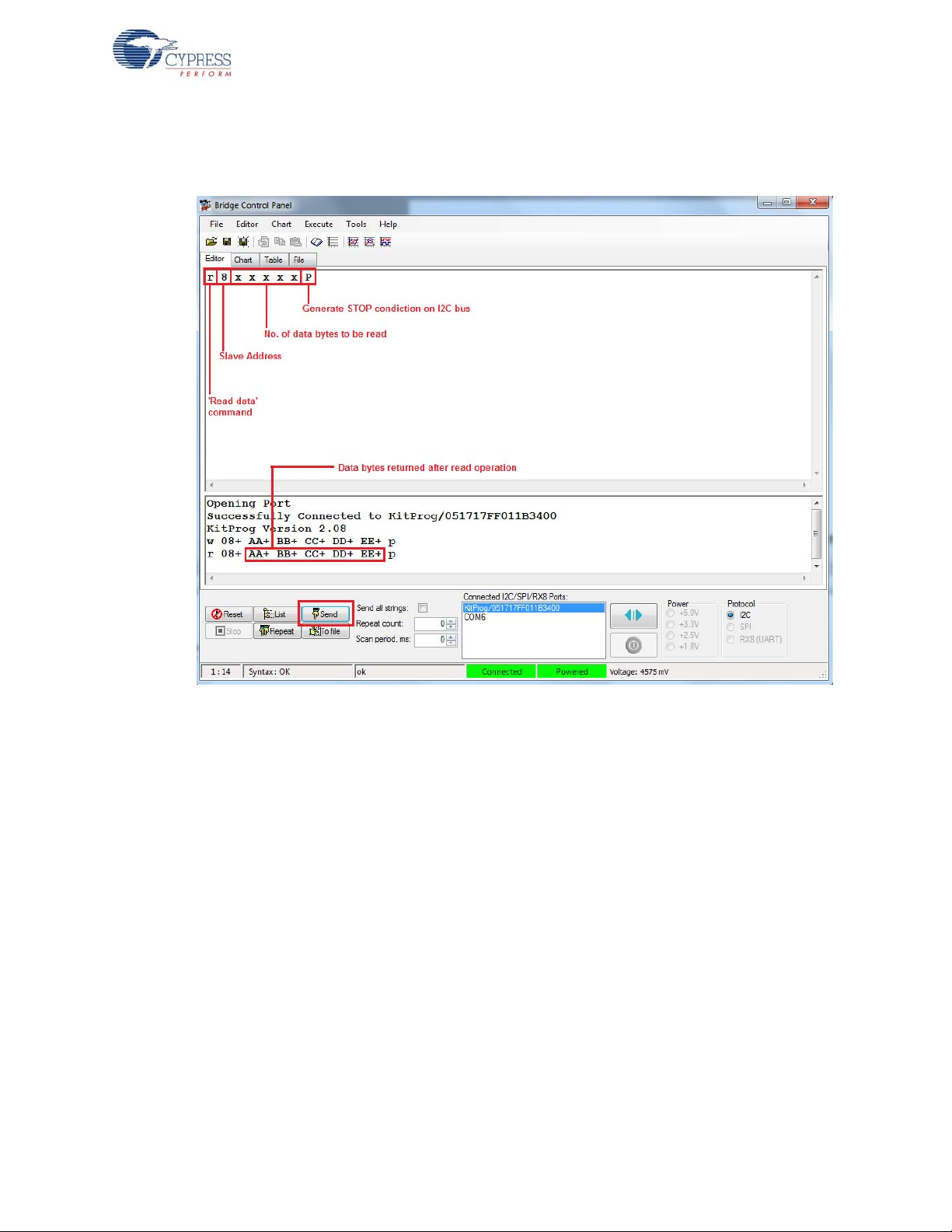
12.From the BCP, read five bytes of data from the I2C slave device with slave address 0x08. The log
shows whether the transaction was successful, as shown in Figure 6-25.
Figure 6-25. Read Data Bytes from BCP
Note: Refer to Help Contents under Help in BCP or press [F1] for details of I
2
C commands.
CY8CKIT-042-BLE Bluetooth® Low Energy (BLE) Pioneer Kit Guide, Doc. # 001-93731 Rev. *A 133

6.3 Developing Applications for PSoC 5LP
The BLE Pioneer kit has an onboard PSoC 5LP whose primar y function is that of a programmer and
a bridge. You can build either a normal project or a bootloadable project using the PSoC 5LP.
The PSoC 5LP connections in the Pioneer board are summarized in Figure 6-26. J8 is the I/O
connector. The USB (J13) is connected and used as the PC interface. However, you can still use this
USB connection to create customized USB designs.
Figure 6-26. PSoC 5LP Connections on BLE Pioneer Kit
Advanced Topics
The programming header (J7) is meant for standalone programming. This header needs to be
populated. See the 'No Load Components' section in Bill of Materials (BOM) on page 184.
6.3.1 Building a Bootloadable Project for PSoC 5LP
All bootloadable applications developed for the PSoC 5LP should be based on the bootloader hex
file, which is programmed onto the kit.
The hex files are included in the following kit installer directory:
<Install_Directory>\CY8CKIT-042-BLE Kit\<version>\Firmware\Programmer\
KitProg_Bootloader
Figure 6-27. KitProg Bootloader Hex File Location
CY8CKIT-042-BLE Bluetooth® Low Energy (BLE) Pioneer Kit Guide, Doc. # 001-93731 Rev. *A 134

Advanced Topics
To build a bootloadable application for the PSoC 5LP, follow this procedure:
1. In PSoC Creator, choose
New > Project > PSoC 5LP, click the expand button adjacent to
Advanced, select Launch Device Selector to bring up the Select Device Window and select
the
Device as CY8C5868LTI-LP039, as shown in Figure 6-28. Select the Application Type as
Bootloadable from the drop-down list and click OK.
Figure 6-28. Create New Project in PSoC Creato r_PSoC 5LP
CY8CKIT-042-BLE Bluetooth® Low Energy (BLE) Pioneer Kit Guide, Doc. # 001-93731 Rev. *A 135

Figure 6-29. Select Device in PSoC Creator
Advanced Topics
2. Navigate to the Schematic view and drag and drop a Bootloadable component (Figure 6-30) on
the TopDesign.
Figure 6-30. Bootloadable Component in Component Catalog
CY8CKIT-042-BLE Bluetooth® Low Energy (BLE) Pioneer Kit Guide, Doc. # 001-93731 Rev. *A 136

Advanced Topics
To configure the Bootloadable, double-click or right-click the Bootloadable component and select
Configure. In the General tab, enable the check box for Manual application ima ge placement and
set the
Placement address to ‘0x00002800’.
Figure 6-31. Configuration Window of Bootloadable Component in “General” Tab Setting
Set the dependency of the Bootloadable component by selecting the
configuration window and clicking the
Browse button, as shown in Figure 6-32. Select the
Dependencies tab in the
KitProg_Bootloader.hex (Figure 6-33) and KitProg_Bootloader.elf files (Figure 6-34); click Open.
Figure 6-32. Configuration Window of Bootloadable Component in the Dependencies Tab
CY8CKIT-042-BLE Bluetooth® Low Energy (BLE) Pioneer Kit Guide, Doc. # 001-93731 Rev. *A 137

Figure 6-33. Select KitProg Bootloader Hex File
Advanced Topics
Figure 6-34. Select KitProg Bootloader Elf File
3. Develop your custom project.
CY8CKIT-042-BLE Bluetooth® Low Energy (BLE) Pioneer Kit Guide, Doc. # 001-93731 Rev. *A 138

Advanced Topics
4. Make sure that the NV L setting of the Bootloa dab le pr oject and the KitPr og_Bootlo ade r project is
the same. Figure 6-35 shows the
KitProg_Bootloader.cydwr system settings.
Figure 6-35. KitProg Bootloader System Settings
5. Build the project in PSoC Creator by choosing
Build > Build Project or [Shift] [F6].
6. To download the project onto the PSoC 5LP device, open the Bootloader Host tool, which is
available in PSoC Creator. Choose
Tools > Bootloader Host, as shown in Figure 6-36.
Figure 6-36. Open Bootloader Host Tool in PSoC Creator
CY8CKIT-042-BLE Bluetooth® Low Energy (BLE) Pioneer Kit Guide, Doc. # 001-93731 Rev. *A 139

Advanced Topics
7. In the Bootloader Host tool, click Filters and add a filter to identify the USB device. Ensure that
the check box for
Show USB Devices is enabled. Set VID as 0x04B4, PID as 0xF13B, and click
OK, as shown in Figure 6-37.
Figure 6-37. Port Filters Tab in Bootloader Host Tool
CY8CKIT-042-BLE Bluetooth® Low Energy (BLE) Pioneer Kit Guide, Doc. # 001-93731 Rev. *A 140

Advanced Topics
8. In the Bootloader Host tool, click the Open File button (Figure 6-38) to browse to the location of
the bootloadable file (*.cyacd), as shown in Figure 6-38.
Figure 6-38. Open Bootloadable File in Bootloader Host Tool
Figure 6-39. Select Bootloadable .cyacd File in Bootloader Host
9. Keep the reset switch (
SW1) pressed and plug in the USB mini-B connector. If the switch is
pressed for more than 100 ms, the PSoC 5LP enters into bootloader. Click the
(Figure 6-38) in the Bootloader Host tool to program the device.
Program button
CY8CKIT-042-BLE Bluetooth® Low Energy (BLE) Pioneer Kit Guide, Doc. # 001-93731 Rev. *A 141

Advanced Topics
10.If bootload is successful, the log of the tool displays “Programming Finished Successfully”;
otherwise, it displays “Failed” and a reason for the failure.
Notes:
■ The PSoC 5LP pins are brought to the PSoC 5LP GPIO header (J8). These pins are selected to
support high-performance analog and digital projects. See PSoC 5LP GPIO Header (J8) on
page 97 for pin information.
■ Take care when allocating the PSoC 5LP pins for custom applicatio ns. For example, P2[0]–P2[4]
are dedicated for programming the PSoC 4 BLE/PRoC BLE. See Schematics on page 168
before allocating the pins.
■ When a custom project is programmed onto the PSo C 5LP, the initial capability of the PSoC 5LP
to act as a programmer, USB-UART bridge, or USB-I
■ The status LED does not function unless used by the custom project.
2
C bridge in not available.
For additional information on bootloaders, refer to Cypress application note, AN73503 -
Bootloader for PSoC 3 and PSoC 5LP
.
USB HID
CY8CKIT-042-BLE Bluetooth® Low Energy (BLE) Pioneer Kit Guide, Doc. # 001-93731 Rev. *A 142

6.3.2 Building a Normal Project for PSoC 5LP
A normal project is a completely new project created for the PSoC 5LP device on the CY8CKIT-042.
Here the entire flash of the PS oC 5LP is programmed, overwriting all bootloader and programming
code. To recover the programmer, reprogram the PSoC 5LP device with the factory-set
file, which is shipped with the kit installer.
KitProg.hex file is available at the following location:
The
<Install_Directory>\CY8CKIT-042-BLE Kit\<version>\Firmware\
Programmer\KitProg
This advanced functionality requires a MiniProg3 programmer, which is not included with this kit. The
MiniProg3 can be purchased from www.cypress.com/go/CY8CKIT-002.
To build a normal project for the PSoC 5LP, follow these steps:
1. In PSoC Creator, choose
Advanced, select Device as CY8C5868LTI-LP039, and select Application Type as Normal
from the drop-down list, as shown in Figure 6-40.
Figure 6-40. Create New Project in PSoC Creato r_PSoC 5LP
New > Project > PSoC 5LP, click the expand button adjacent to
Advanced Topics
KitProg.hex
2. Develop your custom project.
3. Build the project in PSoC Creator by choosing
CY8CKIT-042-BLE Bluetooth® Low Energy (BLE) Pioneer Kit Guide, Doc. # 001-93731 Rev. *A 143
Build > Build Project or pressing [Shift] [F6].

4. Connect the 10-pin connector of MiniProg3 to the onboard 10-pin SWD debug and programming
header J7 (which needs to be populated).
5. To program the PSoC 5LP with PSoC Creator, choose
Debug > Program or press [Ctrl] [F5]. If
the Programming window appears and shows MiniProg3 and the selected device in the project
under it (CY8C5868LTI-LP039); click on the device and click
Connect to program.
Notes:
■ The 10-pin SWD debug and programming header (J7) is not populated. See the 'No Load
Components' section of A.3 Bill of Materials (BOM) for details.
■ The PSoC 5LP pins are brought to the PSoC 5LP GPIO header (J8). These pins are selected to
support high-performance analog and digital projects. See PSoC 5LP GPIO Header (J8) on
page 97 for pin information.
■ Take care when allocating the PSoC 5LP pins for custom applicatio ns. For example, P2[0]–P2[4]
are dedicated for programming the PSoC 4. Refer to A.1 Schematics before allocating the pins.
■ When a normal project is programmed onto the PSoC 5LP, the initial capability of the PSoC 5LP
to act as a programmer, USB-UART bridge, or USB-I
■ The status LED does not function unless it is used by the custom project.
2
C bridge is not available.
6.4 PSoC 5LP Factory Program Restore Instructions
Advanced Topics
The BLE Pioneer Kit features a PSoC 5LP device that comes factory-programmed as the onboard
programmer and debugger for the PSoC 4 BLE/PRoC BLE device.
In addition to creating applications for the BLE device, you can also create custom applications for
the PSoC 5LP device on this kit. For details, see section Developing Applications for PSoC 5LP on
page 134. Reprogramming or bootloading the PSoC 5LP device with a new flash image will
overwrite the factory program and forfeit the ability to use the PSoC 5LP device as a programmer/
debugger for the BLE device. Follow the instructions to restore the factory program on the PSoC
5LP and enable the programmer/debugger functiona lity.
6.4.1 PSoC 5LP is Programmed with a Bootloadable Application
If the PSoC 5LP is programmed with a bootloadable application, restore the factory program by
using one of the following two methods.
6.4.1.1 Restore PSoC 5LP Factory Program Using PSoC Programmer
1. Launch PSoC Programmer 3.21.1 or later from Start > Cypress > PSoC Programmer.
2. Configure the BLE Pioneer Kit in service m ode. To do this, while holding down the reset button
(SW1 Reset), plug in the BLE Pioneer Kit to the computer using the included USB cable (USB A
to mini-B). This puts the PSoC 5LP into service mode, which is indicated by the blinking green
status LED.
CY8CKIT-042-BLE Bluetooth® Low Energy (BLE) Pioneer Kit Guide, Doc. # 001-93731 Rev. *A 144

Advanced Topics
3. The following message appears in the PSoC Programmer Results window, as shown in
Figure 6-41: “KitProg Bootloader device is detected”.
Figure 6-41. PSoC Programmer Results Window
CY8CKIT-042-BLE Bluetooth® Low Energy (BLE) Pioneer Kit Guide, Doc. # 001-93731 Rev. *A 145

Advanced Topics
4. Switch to the Utilities tab in PSoC Programmer and press the Upgrade Firmware button, as
shown in Figure 6-42. Unplug all other PSoC programmers (such as MiniProg3 and DVKProg)
from the PC before pressing the
Upgrade Firmware button.
Figure 6-42. Upgrade Firmware
CY8CKIT-042-BLE Bluetooth® Low Energy (BLE) Pioneer Kit Guide, Doc. # 001-93731 Rev. *A 146

Advanced Topics
5. After programming has completed, the following message appears, as shown in Figure 6-43:
“Firmware Update Finished at <time>”.
Figure 6-43. Firmware Update Completed
6. The factory program is now successfully restored on the PSoC 5LP. It can be used as the
programmer/debugger for the PSoC 4 BLE or PRoC BLE device.
CY8CKIT-042-BLE Bluetooth® Low Energy (BLE) Pioneer Kit Guide, Doc. # 001-93731 Rev. *A 147

6.4.1.2 Restore PSoC 5LP Factory Program Using Bootloader Host Tool
1. Launch the Bootloader Host tool from Start > Cypress > PSoC Creator.
2. Using the
as shown in Figure 6-44. The default location for this file is: <Install_Directory>
CY8CKIT-042-BLE Kit\<version>\Firmware\Programmer\KitProg\KitProg.cyacd
Figure 6-44. Load KitProg.cyacd File
File > Open menu, load the KitProg.cyacd file, which is installed with the kit software,
Advanced Topics
\
CY8CKIT-042-BLE Bluetooth® Low Energy (BLE) Pioneer Kit Guide, Doc. # 001-93731 Rev. *A 148

Advanced Topics
3. Configure the Pioneer Kit in service mode. To do this, while holding down the reset button (SW1
Reset), plug in the BLE Pioneer Kit to the computer using the included USB cable (USB A to
mini-B). This puts the PSoC 5LP into service mode, which is indicated by the blinking green
status LED.
4. In the Bootloader Host tool, set the filters for the USB devices with VID:
The
USB Human Interface Device port appears in the Ports list. Click that port to select it, as
04B4 and PID: F13B.
shown in Figure 6-45.
Figure 6-45. Select USB Human Interface Device
5. Click the
Program button (or choose Actions > Program) to restore the factory-program by
bootloading it onto the PSoC 5LP.
CY8CKIT-042-BLE Bluetooth® Low Energy (BLE) Pioneer Kit Guide, Doc. # 001-93731 Rev. *A 149

Advanced Topics
6. After programming has completed, the following message appears, as shown in Figure 6-46:
“Programming Finished Successfully”.
Figure 6-46. Programming Finished Successfully
7. The factory program is now successfully restored on the PSoC 5LP. It can be used as the
programmer/debugger for the PSoC 4 BLE/PRoC BLE device.
6.5 Using FM24V10 F-RAM
The BLE Pioneer board has an onboard ferroelectric RAM chip that can h old up to 1 Mb of dat a. The
chip provides an I
and P3_5); the same lines are also routed to the PSoC 5LP I
2
an I
C slave, it can be accessed or shared among various I2C masters on the same line. For more
details on the F-RAM device, refer to the device datasheet.
2
C communication interface for data access. It is hardwired to the I2C lines (P3_4
2
C lines. Because the F-RAM device is
CY8CKIT-042-BLE Bluetooth® Low Energy (BLE) Pioneer Kit Guide, Doc. # 001-93731 Rev. *A 150

6.5.1 Address Selection
The slave address of the F-RAM device consists of three parts, as shown in Figure 6-47: slave ID,
device select, and page select. Slave ID is an F-RAM family-specific ID located in the datasheet of
the particular F-RAM device. For the device used in BLE Pioneer board (FM24V10), the slave ID is
1010b. Device select bits are set using the two physical pins A2 and A1 in the device. The setting of
these two pins on the BLE Pioneer board is controlled by resistors R32/R36 (A1) and R33/R37 (A2).
Because the memory location in F-RAM is divided into two pages of 64 KB each, the page select bit
is used to refer to one of the two pages in which the read or write operations will take place.
Figure 6-47. F-RAM I
2
C Address Byte Structure
6.5.2 Write/Read Operation
The device's datasheet includes details on how to perform a write/read operation with the F-RAM.
Figure 6-48 and Figure 6-49 provide a snapshot of the write/read packet structure as a quick
reference.
Advanced Topics
Figure 6-48. F-RAM Single-Byte and Multiple-Byte Write Packet Structure
CY8CKIT-042-BLE Bluetooth® Low Energy (BLE) Pioneer Kit Guide, Doc. # 001-93731 Rev. *A 151

Figure 6-49. F-RAM Single-Byte and Multiple-Byte Read Packet Structure
Advanced Topics
As shown in the figures, all operations start with the slave address followed by the memory address.
For write operations, the bus master sends each byte of data to the memory, and the memory
generates an acknowledgement condition. For read operations, after receiving the complete slave
address and memory address, the memory begins shifting dat a from the curren t address on the next
clock.
6.6 CySmart iOS/Android Application
The CySmart mobile application is a powerful tool that allows the mobile device (iOS/Android) with
BLE capability to connect to a BLE peripheral device and communicate with it. It supports various
standard BLE services along with two custom services for CapSense and LED control. It also
provides a common support for all profiles, standard or custom.
This app is free. You can download and install it for Apple iOS devices from the App Store and for
Android Devices from Play Store. Make sure that the mobile device being used supp orts BLE.
To verify the example project using the CySmart mobile app, follow these steps.
1. Plug the BLE Pioneer Kit into the PC for power, using the J13 USB connector .
2. Program the kit with the desired BLE example project.
3. Open the app on the mobile device.
CY8CKIT-042-BLE Bluetooth® Low Energy (BLE) Pioneer Kit Guide, Doc. # 001-93731 Rev. *A 152

Advanced Topics
4. If Bluetooth is not enabled on the device, the app will ask to enable it, as shown in Figure 6-50.
Figure 6-50. Turn on Bluetooth on Device
5. After Bluetooth is enabled, the app will automatically search for available BLE peripherals and list
them, as shown in Figure 6-51. Select the BLE Pioneer Kit peripheral in the list. The name
displayed in the list will be the same as that set in the BLE Component.
Figure 6-51. Peripheral Connections Page
CY8CKIT-042-BLE Bluetooth® Low Energy (BLE) Pioneer Kit Guide, Doc. # 001-93731 Rev. *A 153

Advanced Topics
6. When connected, the app will list the supported profiles by the peripherals, as shown in
Figure 6-52. Tap on the desired profile.
Figure 6-52. Profiles Page
7. Depending on the type of profile chosen, the app will display options for the profile. Figure 6-53
shows an example for the CapSense slider custom profile, where swiping a finger on the
CapSense slider of the BLE Pioneer Kit is reflected in the app. See Pioneer Baseboard on
page 88.
Figure 6-53. CapSense Slider GUI
8. To go to a different service, go back to the service page in the GUI.
CY8CKIT-042-BLE Bluetooth® Low Energy (BLE) Pioneer Kit Guide, Doc. # 001-93731 Rev. *A 154

Advanced Topics
9. To connect to a new BLE pe ripheral, go back to home page and swip e the screen be low to scan
for devices.
10.To transfer data/notifications through any other profile that is not listed on the Profiles page after
connecting to the peripheral, go to the
GATT DB option on the Profiles page. The GATT DB
allows you to access the services and characteristics of a profile directly, as shown in
Figure 6-54, and to modify or receive values through BLE.
Figure 6-54. GATT DB GUI for Characteristics
The
Data Logger option provide s a te xtual for m of all t he even t s that has happened with a p a rticular
BLE peripheral device, including scanning and connection.
Figure 6-55. Data Logger
CY8CKIT-042-BLE Bluetooth® Low Energy (BLE) Pioneer Kit Guide, Doc. # 001-93731 Rev. *A 155

Advanced Topics
Two custom profiles are created for demonstrating the BLE Pioneer Kit features: the CapSense
profile and the RGB LED profile. Both these profiles are integrated into the CySmart mobile app, as
easy-to-use GUI.
The CapSense profile GUI supports three CapSense functiona lities.
■ CapSense Buttons: After connecting to the BLE peripheral, the CapSense Buttons service page
displays the number of CapSense buttons supported by the peripheral, as shown in Figure 6-56.
Any touch on one of the CapSense buttons on the peripheral is reflected in the CySmart GUI.
Figure 6-56. CapSense Buttons GUI Page
CY8CKIT-042-BLE Bluetooth® Low Energy (BLE) Pioneer Kit Guide, Doc. # 001-93731 Rev. *A 156

Advanced Topics
■ CapSense Slider: After connecting to the BLE peripheral, the CapSense Slider service page
displays the CapSense slider as supported by the peripheral, as shown in Figure 6-57. Swiping a
finger on the CapSense slider on the peripheral is reflected in the CySmart GUI.
For example, the CapSense_Slider_LED project (CapSense Slider and LED on page47) will
show this utility on the app.
Figure 6-57. CapSense Slider GUI Page
CY8CKIT-042-BLE Bluetooth® Low Energy (BLE) Pioneer Kit Guide, Doc. # 001-93731 Rev. *A 157

Advanced Topics
■ CapSense Proximity: After connecting to the BLE peripheral, the CapSense Proximity service
page displays the CapSense proximity supported by the peripheral, as shown in Figure 6-58. A
change in proximity on the proximity sensor (such as a wire) on the peripheral is reflected in the
CySmart GUI.
For example, the CapSense_Proximity project (CapSense Proximity on page 62) will show this
utility on the app.
Figure 6-58. CapSense Proximity GUI Page
CY8CKIT-042-BLE Bluetooth® Low Energy (BLE) Pioneer Kit Guide, Doc. # 001-93731 Rev. *A 158

Advanced Topics
The RGB LED profile allows you to control the color and intensity of the BLE Pioneer Kit onboard
RGB LED, as shown in Figure 6-59. Pressing any part of the color gamut on the GUI is reflected on
the BLE peripheral device with the onboard RGB LED.
Note: The onboard RGB LED color range depends on the LED being used. It is possible that the
complete color gamut is not reflected on the onboard RGB LED due to limitations on the LED itself.
For example, the CapSense_Slider_LED project (CapSense Slider and LED on page 47) will show
this utility on the app.
Figure 6-59. RGB LED Profile
CY8CKIT-042-BLE Bluetooth® Low Energy (BLE) Pioneer Kit Guide, Doc. # 001-93731 Rev. *A 159

6.7 CySmart PC Tool
The CySmart PC tool is a BLE Central host emulation tool that, along with the dongle, allows you to
connect to a BLE peripheral device and transfer data over BLE services. Also, it displays all the
packets that are involved during the connection, which can be analyzed for details.
The CySmart PC tool is installed as part of the BLE Pioneer Kit installer. To launch the software,
choose
Follow these steps to connect to a BLE peripheral device using the dongle and CySmart PC tool and
to transfer data.
1. Connect the dongle to one of the USB ports on the PC.
Figure 6-60. Connect Dongle to USB Port
Start > All Programs > Cypress > CySmart <version> > CySmart <version>.
Advanced Topics
CY8CKIT-042-BLE Bluetooth® Low Energy (BLE) Pioneer Kit Guide, Doc. # 001-93731 Rev. *A 160

Advanced Topics
2. Start the CySmart PC tool on the PC. You will see a list of dongles connected to it. Select the
dongle you want to use and click
Connect, as shown in Figure 6-61.
Figure 6-61. Selecting Dongle in CySmart PC Tool
3. The CySmart PC tool can be used to connect to any BLE peripheral device, including the BLE
Pioneer kit. To connect to the BLE Pioneer kit, power the kit through the J13 USB connector and
program the appropriate BLE peripheral project to it. Follow the steps according to the project
description to start advertising.
CY8CKIT-042-BLE Bluetooth® Low Energy (BLE) Pioneer Kit Guide, Doc. # 001-93731 Rev. *A 161

Advanced Topics
4. When the dongle is selected and connected to, the main window shown in Figure 6-62 opens up.
Figure 6-62. CySmart PC Tool Main Window
The important parts of this window are as follows:
■ Menu bar: This contains options to exit or find help about the CySmart PC tool.
■ Dongle settings: These settings comprise of Select Dongle, Configure Master Settings, and
Manage PSMs. Select the dongle allows to connect to a dongle that is listed by the system. If a
different dongle needs to be connected, then this option can be used. Configure Master Settings
option allows to modify the various settings that the dongle requires to act as a BLE Central
device such as connection parameters, scan parameters, or security parameters. Manage PSMs
allows to register for PSM or modify them.
■ Discovered devices options: The Master tab provides three options by default: Start Scan ,
Connect, and Add to Whitelist. The Start Scan button allows the tool to start scanning for
available BLE peripheral devices and list them in the Discovered Devices window. This option
also allows to stop an ongoing scan. The Connect option allows to connect to a particular BLE
peripheral device that is listed in the D iscove red D evice windo w. Add to Whitelist allows to add a
selected device address to the whitelist.
■ Advertisement Data/Scan response data tabs: These tabs provide the description of the data
received in the advertisement packet and scan response packet from the selected device.
■ Discovered Devices window: This window lists all the peripheral devices found after starting a
scan. Selecting any device populates the information on advertisement data and scan response
data on the right side window.
■ Whitelist window: This window lists the devices that have been added as whitelist and provides
options to add, remove, or clear devices from the whitelist.
■ Raw Data window: This window displays the raw data (in hexadecimal) of the field selected.
■ Log window: This window displays all the activities that occur on the dongle and the data
communicated. This feature is also useful for debugging.
CY8CKIT-042-BLE Bluetooth® Low Energy (BLE) Pioneer Kit Guide, Doc. # 001-93731 Rev. *A 162

Advanced Topics
1. Click Start Scan to see the list of available BLE peripheral devices, as shown in Figure 6-63.
Figure 6-63. Scanned Devices Listed in CySmart PC Tool
2. After the available devices are listed, choose the desired peripheral and double-click
as shown in Figure 6-64.
Figure 6-64. Start Connection with Selected Device
Connect,
CY8CKIT-042-BLE Bluetooth® Low Energy (BLE) Pioneer Kit Guide, Doc. # 001-93731 Rev. *A 163

Advanced Topics
3. If the connection is successful, you will see another tab opening besides the Master tab. This tab
provides options with respect to the connected BLE device, as shown in Figure 6-65.
Figure 6-65. Connected Device Tab
4. On the device tab, click
Discover All Attributes to find the supported attributes by the connected
BLE device. This action populates the list of services and characteristics in the Attribute window
along with their values, if any, as shown in Figure 6-66.
Figure 6-66. Discover All Attributes
CY8CKIT-042-BLE Bluetooth® Low Energy (BLE) Pioneer Kit Guide, Doc. # 001-93731 Rev. *A 164

Advanced Topics
5. You can read the characteristics individually or you can use the Read All Characteristics option
to update the values for all readable characteristics, as shown in Figure 6-67.
Figure 6-67. Read All Characteristics
6. To modify the value of a characteristic individually, select the particular characteristic from the
attribute list. The Attribute Details window on the right will display the properties of the selected
characteristics as well as the options to modify or read the values, as shown in Figure 6-68.
Figure 6-68. Modify a Characteristic
7. Similarly, notifications or indications can be enabled on the characteristics that support those
properties.
CY8CKIT-042-BLE Bluetooth® Low Energy (BLE) Pioneer Kit Guide, Doc. # 001-93731 Rev. *A 165

Advanced Topics
8. The list of attributes of the connected BLE device can also be saved in .csv format for later use.
For this, click the
Export button on the device tab and select the location where you want the file
to be saved, as shown in Figure 6-69.
Figure 6-69. Save Attribute List to a File
9. The tool also allows sending specific commands to the BLE peripheral device. These commands
are present in the
from the list and click
Send Commands tab on the device window. Select the command to be sent
Send, as shown in Figure 6-70.
Figure 6-70. Send Commands
CY8CKIT-042-BLE Bluetooth® Low Energy (BLE) Pioneer Kit Guide, Doc. # 001-93731 Rev. *A 166

Advanced Topics
10.To disconnect from the device, go to the Master tab, select the connected device, and click
Disconnect, as shown in Figure 6-71.
Figure 6-71. Disconnect BLE Device
Note: Refer to the CySmart PC tool user guide for more information. To access the u ser gui de from
the tool, go to
Help > Help Topics.
CY8CKIT-042-BLE Bluetooth® Low Energy (BLE) Pioneer Kit Guide, Doc. # 001-93731 Rev. *A 167

A. Appendix
SAR Bypass
Capacitor
Del Sig Bypass
Capacitor
PSoC 5LP Programmer / Debugger
NO LOAD
NO LOAD
SAR Bypass
Capacitor
P5LP0_4 to P5LP0_7,
P5LP3_2, P5LP3_3 are
reserved for HW REV ID
NO LOAD
VSSD
P5LP_SWDCLK
P5LP_SWDIO
P5LP_SWO
P5LP_TDI
P5LP_XRES
P5LP_XRES
P5LP_DP
P5LP_DM
P5LP0_3
DM_P
DP_P
P5LP0_0
P5LP0_1
P5LP12_0
P5LP12_1
P5LP12_6
VSSD
VSSD
P5LP12_7
P5LP12_2
P5LP2_6
P5LP2_7
P5LP12_4
P5LP1_2
P5LP3_7
P5LP3_6
P5LP0_2
VSSD
P5LP12_3
P5LP3_0
P5LP3_4
P5LP3_5
P5LP1_7
P5LP1_6
P5LP3_1
P5LP_VCCD
P5LP12_5
P5LP0_4
P5LP0_6
P5LP_VCCD
P5LP2_5
P5LP1_5
P5LP_VDD
P5LP_VDD
P5LP_VDDP5LP_VDD
P5LP_VDD
P5LP_VDD
P5LP_VDD
VTARG P5LP_VDDVBUS
P5LP_VDD
VBUS
P5LP_DP
P5LP_DM
EN_CTRL
R18
15K
R24
30K
R25
30K
0402
C22
0.1 uF
0603
C6
1.0 uF
0402
C17
0.1 uF
0603
C13
1.0 uF
R21
4.7K
0603
C11
1.0 uF
0603
R1522E
R17
15K
0603
C20
1.0 uF
0402
C21
0.1 uF
0603
C15
1.0 uF
0402
C8
0.1 uF
0603
C24
1.0 uF
U2
CY8C5868LTI-LP039 QFN68
P2_6
1
P2_7
2
P12_4 I2C0_SCL, SIO
3
P12_5 I2C0_SDA, SIO
4
VSSB
5
IND
6
VBOOST
7
VBAT
8
VSSD
9
XRES
10
P1_0
11
P1_1
12
P1_2
13
P1_3
14
P1_4
15
P1_5
16
VDDIO1
17
P1_618P1_719P12_6_SIO20P12_7_SIO21P15_6 DP22P15_7 DM23VDDD24VSSD25VCCD26P15_027P15_128P3_029P3_130P3_231P3_332P3_433P3_5
34
VDDIO3
35
VDDIO0
52
P0_3
51
P0_2
50
P0_1
49
P0_0
48
SIO_P12_3
47
SIO_P12_2
46
VSSD
45
VDDA
44
VSSA
43
VCCA
42
P15_3
41
P15_2
40
SIO, I2C1_SDA P12_1
39
SIO, I2C1_SCL P12_0
38
P3_7
37
P3_6
36
P2_466P2_365P2_264P2_163P2_0
62
P15_561P15_460VDDD
59
VSSD
58
VCCD
57
P0_756P0_655P0_554P0_4
53
VDDIO2
67
P2_5
68
EPAD
69
0603
R1622E
0402
C10
0.1 uF
0603
C7
1.0 uF
0402
C18
0.1 uF
0402
C9
0.1 uF
0603
C16
1.0 uF
0402
C19
0.1 uF
0402
C14
0.1 uF
R14 ZERO
PSoC 4 / External PSoC Program/Debug HeaderPSoC 5LP Program/Debug Header
NO LOAD NO LOAD
P5LP12_2
P5LP12_3
P5LP12_4
P5LP_SWO
P5LP_XRES
P5LP_SWDCLK
P5LP_TDI
P5LP_SWDIO
VTARGP5LP_VDD
RESET
SWDCLK
SWDIO
0402
C5
0.1 uF
TVS2
5V 350W
TVS1
5V 350W
J7
50MIL KEYED SMD
1
3
5
7
9
2
4
6
8
10
J6
50MIL KEYED SMD
1
3
5
7
9
2
4
6
8
10
0402
C12
0.1 uF
A.1 Schematics
A.1.1 BLE Pioneer Board
CY8CKIT-042-BLE Bluetooth® Low Energy (BLE) Pioneer Kit Guide, Doc. # 001-93731 Rev. *A 168

PSoC 5LP GPIO Expansion Header
USB-Serial Bridge Connections
P5LP12_6 ------------- UART RX
P5LP12_7 ------------- UART TX
P5LP12_0 ------------- SPI SCLK / I2C SCL
P5LP12_1 ------------- SPI MISO / I2C SDA
P5LP12_5 ------------- SPI MOSI
P5LP2_5 ------------- SPI SSEL
P5LP12_7P5LP12_6
P5LP3_6 P5LP3_7
P5LP0_0
P5LP1_2
P5LP3_5P5LP3_4
P5LP3_0
P5LP0_1
P5LP12_1
P5LP12_5P5LP12_0
P5LP2_5
VDD
SPI_MOSI
SPI_SSEL
UART TXUART RX
J8
8x2 RECPT
112
2
334
4
556
6
778
8
10109
9
121211
11
141413
13
161615
15
I2C Connection
Status LED
P5LP3_1
SCL
SDA
P5LP12_0
P5LP12_1
P5LP2_7
P5LP2_6
VDD
SPI_MISO / I2C_SDA
SPI_SCLK / I2C_SCL
U4
NTZD3152P
6
2
1
3 4
5
R23
2.2K
R27 ZERO
R11
820 ohm
R26 ZERO
0805
LED2
Status LED Green
2 1
R22
2.2K
USB MiniB
NO LOAD
NO LOAD
CR2032 Coin Cell
Battery Holder
DP
DM
VDD
VBUS
VIN
P5LP_DM
P5LP_DP
J13
USB MINI B
VBUS
1
DM
2
DP
3
GND
5
ID
4
S16S2
7
F1
PTC Resettable Fuse
1 2
C4
100uF
0603
D6
SOD123
D10
0402
R6100K
0603
D8
0402
C3 0.01 uF
J9
2 PIN HDR
1
1
2
2
+
-
BT1
1
3 2
TP2 RED
0603
D7
CY8CKIT-042-BLE Bluetooth® Low Energy (BLE) Pioneer Kit Guide, Doc. # 001-93731 Rev. *A 169

NO LOAD
Protection Circuit
NO LOAD
VDDV3.3
VFRAMVDD
R9
10K
R59 ZERO
Q2
PMOS( NTR4171PT1G)
R8
15K
D11
Vz=2.7V(MMSZ 4682T1G)
Q5
PMOS( PMV48XP,215)
D9
Vz=3.9V(BZT 52C3V9-7-F)
R7 ZERO
R20
10K
Q6
PMOS( NTR4171PT1G)
R58
15K
Q4
PMOS( NTR4171P T1G)
Q3
PMOS(PMV48XP,215)
Q1
PMOS( DMP3098L-7)
NO LOAD NO LOAD
1
2
3
4
5
6
CTL
VCC
N.C.
OUT
C
GND
Output Voltage ON / OFF control
Power supply voltage input
Unconnected terminal
Voltage output
Output voltage regulation terminal
Ground
Pin No Symbol Function.
TABLE: LDO PIN FUNCTIONS
GND Test Points
TABLE: VOLTAGE SELECTION JUMPER SETTINGS
JUMPER SETTING O/P VOLTAGE
SHORT 2 & 3
SHORT 1 & 2
REMOVE JUMPER
3.3V
5V
1.9V
VADJ VDD
VCC
EN_CTRL
EN_CTRL
VBUS
VIN
VCC
EN_CTRL
TP5
BLACK
U1
BA00BC0WFP-E2
VCC
2
CTL
1
NC
3
OUT
4
C
5
GND
6
SOD123
D1
R1
11K
1%
R10
10K
+
3216
C2
4.7uF
R4
10K 1%
SOD123
D4
R3
14.7K 1%
R5
4.3K 1%
TP6
BLACK
SOD123
D2
J16
3 PIN HDR
1
3
2
TP4
BLACK
+
3216
C1
1 uFd
SOD123
D3
CY8CKIT-042-BLE Bluetooth® Low Energy (BLE) Pioneer Kit Guide, Doc. # 001-93731 Rev. *A 170

NO LOAD
NO LOAD
Current Measurement Jumper
VADJ
VDD BLE_VDD
VTARG
R2
560 ohm
J15
HDR2
1
2
R44 ZERO
R45 ZERO
TP1 RED
0805
LED1
Power LED
2 1
(J1- J4) Arduino Connectors
J12 Arduino ICSP compatible header
for SPI Interface
NO LOAD
GND
/XRES
/XRES
P1_4
P1_5
P1_6
P1_7
P1_3
P1_2
P1_1
P1_0
P3_5
P3_4
P3_3
P3_2
P3_1
P3_0
P0_5
P0_4
P0_2
P0_0
P0_1
P0_3
VREF
P0_1
P0_3 P0_0
P2_0
P2_1
P2_2
P2_3
P2_4
P2_5
P3_5
P3_4
BLE_VDD
VIN
V3.3
VBUS
J2
CON6X2
A0
1
A1
3
A2
5
A3
7
A4
9
A5
11
P2.0
2
P2.1
4
P2.2
6
P2.3
8
P2.4
10
P2.5
12
J4
CON8
D0
1
D1
2
D2
3
D3
4
D4
5
D5
6
D6
7
D7
8
J3
CON10
D8
1
D9
2
D10
3
D11
4
D12
5
D13
6
GND
7
AREF
8
SDA
9
SCL
10
J12
3x2 RECPT
1 2
3 4
5 6
SOD123
D5
J1
CON8
VIN
1
GND
2
GND
3
V5.0
4
V3.3
5
Reset
6
IORef
7
NC
8
PSoC 4 BLE/PRoC BLE I/O Headers
NO LOAD
Analog PinsDigital Pins
VDDA
P3_7P3_6
P3_5P3_4
P3_3P3_2
P3_1P3_0
P5_1P4_0
P5_0P4_1
P2_7P2_6
P2_5P2_4
P2_3P2_2
P2_1P2_0
GNDVDDR
GND
VDDD
P1_7
P1_5
P1_3
P0_5
P0_3
P0_1
P0_4
P0_2
P0_0
P1_6
/XRES
P1_0
P1_1 P1_2
P1_4
P0_7
P0_6
VREF
GND
VDDR
VDDD
VDDA
BLE_VDD
L1
330 OHM @ 100MHz
J11
HEADER 10x2
1 2
3 4
5 6
7 8
9 10
11 12
13 14
15 16
17 18
19 20
TP3
RED
J10
HEADER 12x2
1 2
3 4
5 6
7 8
9 10
11 12
13 14
15 16
17 18
19 20
21 22
23 24
0402
C28
0.1 uF
0402
C26
0.1 uF
L2
330 OHM @ 100MHz
0402
C27
0.1 uF
L3
330 OHM @ 100MHz
CY8CKIT-042-BLE Bluetooth® Low Energy (BLE) Pioneer Kit Guide, Doc. # 001-93731 Rev. *A 171

Shield Setting
RESET
NO LOAD
USER SWITCH
SHIELD
GND
P1_6
P3_6
P3_7
P2_6
P2_7
P2_1
P2_2
P2_3
P2_4
P2_5
/XRES
BLE_VDD
/XRES
R39 560 ohm
R42 560 ohm
CSS1
CapSense Slider 5 Seg
5
4
3
2
1
R30 1.5K
R13 ZERO
0402
C25
0.1 uF
R12 ZERO
R43 560 ohm
R41 560 ohm
SW2
EVQ-PE105K
1 2
R40 560 ohm
R28 2.2K R29 1.5K
RG
B
LED3
RGB LED
1
2 3
4
SW1
EVQ-PE105K
1 2
F-RAM
NO LOAD NO LOAD NO LOAD
A1
A2
A1
P5_0
P5_1
WP
A2 WP
VFRAM
VFRAM
VFRAM VFRAM
VFRAM
VFRAM
R32
ZERO
R37
ZERO
U3
FM24V10
A1
2
VSS
4
SCL
6
VDD
8
NC
1
A2
3
SDA
5
WP
7
C29
33uF
R36
ZERO
R35
2.2K
0402
C23
0.1 uF
R33
ZERO
R34
ZERO
R38
ZERO
R31
2.2K
Proximity Header
PMOD Connector
NO LOAD
P0_2
P0_0
P0_1
P0_3
P2_0
VDD
J14
1x1 RECP
J5
CON6
SS
1
MOSI
2
MISO
3
SCK
4
GND
5
VCC
6
R19 ZERO
NO LOAD
USB-I2C
USB-SPI
USB-UART
USB-SWD
PSoC 5LP and PSoC 4 BLE/PRoC BLE Connections
NO LOAD
NO LOAD
NO LOAD
P0_3
P0_1
P0_2
P0_0
P3_5
P3_4
/XRES
P0_7
P0_6
P1_5
P1_4
SPI_MOSI
SPI_SSEL
SPI_MISO / I2C_SDA
SPI_SCLK / I2C_SCL
RESET
SWDIO
SWDCLK
UART TX
UART RX
R52 ZERO
R53 ZERO
R54 ZERO
R49 ZERO
R50 ZERO
R56 ZERO
R46 ZERO
R55 ZERO
R48 ZERO
R51 ZERO
R47 ZERO
CY8CKIT-042-BLE Bluetooth® Low Energy (BLE) Pioneer Kit Guide, Doc. # 001-93731 Rev. *A 172

A.1.2 BLE Module
SAR bypass
CMOD
Shunt
Resistor
C_Tank
KHz Crystal
MHz Crystal
TX
RX
Analog Pins
Serial Interface
No Load
No Load
No Load
No Load
No Load
Digital Pins
No Load
PCA: 121-60159-01
PCB: 600-60195-01
FAB DRW: 610-60187-01
ASSY DRW: 620-60195-01
No Load
No Load
No Load
No Load
No Load
P4.0 P4.1
P6.0
P6.1
XTAL24O
XTAL24I
P6.0
P6.1
/XRES
P4.0
P4.1
P5.0
P5.1
XTAL24I
XTAL24O
P2.6
P2.7
P3.0
P3.1
P3.2
P3.3
P3.4
P3.5
P3.6
P3.7
P1.5
P1.4
/XRES
P1.6
P1.5
P1.4
P1.3
P1.2
P1.1
P2.4
P2.3
P2.2
P2.1
P2.0
P1.7
P2.5
P3.7P3.6
P3.5P3.4
P3.3P3.2
P3.1P3.0
P5.1P4.0
P5.0P4.1
P2.7P2.6
P2.5P2.4
P2.3P2.2
P2.1P2.0
P1.7
P1.5
P1.3
P0.5
P0.3
P0.1
P0.4
P0.2
P0.0
P1.6
/XRES
P1.0
P1.1 P1.2
P1.4
P0.7
P0.6
P0.0
P0.1
P0.2
P0.3
P0.4
P0.5
P0.6
P0.7
P1.0
VDDD
VDDA
VDDR
VCCD
VDDD
VREF
VDDR
VDDA VREF
VDDR VDDDVDDA
VDDD
VCCD VDDD
VDDA
VDDA
VDDR
VDDD
VREF
VDDD
Title
CYPRESS SEMICONDUCTOR © 2014
CY8CKIT-142 PSoC 4 BLE Module
Title
CYPRESS SEMICONDUCTOR © 2014
CY8CKIT-142 PSoC 4 BLE Module
Title
CYPRESS SEMICONDUCTOR © 2014
CY8CKIT-142 PSoC 4 BLE Module
0603
C10
1.0 uF
0402
C9
0.1 uF
C13
1.2 pF
0603
C20
1.0 uF
J2
HEADER 10x2
1 2
3 4
5 6
7 8
9 10
11 12
13 14
15 16
17 18
19 20
0603
C2
1.0 uF
L4
330 OHM @ 100MHz
0402
C1
0.1 uF
TP2
RED
C23
36 pF
C22
10000 pF
0603
C4
1.0 uF
0603
C25
100 pF
0603
C17
1.0 uF
0603
C6
1.0 uF
0402
C3
0.1 uF
0402
C16
0.1 uF
0402
C5
0.1 uF
C21
2200 pF
L3
330 OHM @ 100MHz
TP1
RED
0603
C8
1.0 uF
0603
C19
1.0 uF
R1
Zero Ohm
0402
C18
0.1 uF
0603
C15
1.0 uF
J3
4 HEADER
1
2
3
4
R2
Zero Ohm
L1
6.8nH
0603
C12
1.0 uF
C24
18 pF
TP3
RED
0402
C11
0.1 uF
Y1
32.768KHz
12
TP5
BLACK
CY8C4247LQI-BL483
U1
VDDD
1
XTAL32O/P6.0
2
XTAL32I/P6.1
3
XRES
4
P4.0
5
P4.1
6
P5.0
7
P5.1
8
VSSD
9
VDDR
10
GANT1
11
ANT
12
GANT2
13
VDDR
14
P2.5
42
P2.4
41
P2.3
40
P2.2
39
P2.1
38
P2.0
37
VDDA
36
P1.7
35
P1.6
34
P1.5
33
P1.4
32
P1.3
31
P1.2
30
P1.1
29
EPAD
57
VCCD
56
VSSA
55
P3.754P3.653P3.552P3.451P3.350P3.249P3.148P3.0
47
VDDA
46
VREF
45
P2.744P2.6
43
VDDR15XTAL24I16XTAL24O17VDDR
18
P1.0
28
P0.019P0.120P0.221P0.322VDDD23P0.424P0.525P0.626P0.7
27
Y2
24Mhz
1
234
TP4
RED
R3
4.7K
L2
330 OHM @ 100MHz
J1
HEADER 12x2
1 2
3 4
5 6
7 8
9 10
11 12
13 14
15 16
17 18
19 20
21 22
23 24
J4
50 Ohm Wiggle Antenna
11
22
C14
1.5 pF
0402
C7
0.1 uF
CY8CKIT-042-BLE Bluetooth® Low Energy (BLE) Pioneer Kit Guide, Doc. # 001-93731 Rev. *A 173

A.1.3 Dongle
NO LOAD
NO LOAD
I2C Connection
Power and Status LED
USB A PLUG
NO LOAD
USB Connection
PSoC 5LP Programmer / Debugger
NO LOAD NO LOADNO LOAD
PCA: 121-60161-01
PCB: 600-60197-01
FAB DRW: 610-60189-01
ASSY DRW: 620-60197-01
SAR Bypass
Capacitor
P5LP0_4 to P5LP0_7,
P5LP3_2, P5LP3_3 are
reserved for HW REV ID
NO LOAD
SAR Bypass
Capacitor
Del Sig Bypass
Capacitor
PRoC Program/Debug Header
NO LOAD NO LOAD NO LOAD
PSoC 5LP and PRoC BLE Connections
P5LP12_0
P5LP12_1
P5LP_XRES
P5LP2_7
P5LP2_6
SCL
SDA
DM
DP
P5LP_SWDIO
P5LP_SWDCLK
P5LP3_1
P5LP_POWER
P5LP_XRES
P5LP0_4
VSSD
P5LP_SWDCLK
P5LP_SWDIO
P5LP_SWO
P5LP12_5
P5LP_XRES
P5LP_DP
P5LP_DM DM_P
P5LP0_3
DP_P
P5LP0_0
P5LP0_1
P5LP12_0
P5LP12_6
P5LP12_1
VSSD
VSSD
P5LP12_7
P5LP2_6
P5LP2_7
P5LP12_4
P5LP3_7
P5LP3_6
P5LP0_2
VSSD
P5LP3_0
P5LP12_3
P5LP3_4
P5LP3_5
P5LP1_7
P5LP1_6
P5LP3_1
P5LP_VCCD
P5LP_POWER
P5LP_VCCD
P5LP2_5
P5LP0_5
P5LP15_4
P5LP1_2
P5LP12_2
P5LP12_2
P5LP12_3
P5LP12_4
SWDIO
SWDCLK
/XRES
P5LP12_5
P5LP12_1
P5LP2_5
P5LP12_0
P5LP12_7
P5LP12_6
VBUS
P5LP15_4
P5LP_VDD
P5LP_VDD
VBUS
VTARG
VBUS
VTARG
VBUS
P5LP_VDD
P5LP_VDD
P5LP_VDD
P5LP_VDD
P5LP_VDD
P5LP_VDD
P5LP_VDD
VTARGVBUS
VTARG
SDA
SCL
P5LP_DM
P5LP_DP
P5LP_DP
P5LP_DM
EXTRA
/XRES
SWDCLK
SWDIO
P5LP12_5
P5LP12_1
P5LP2_5
P5LP12_0
P5LP12_6
P5LP12_7
Title
Size
Document Number Rev
CYPRESS SEMICONDUCTOR © 2014
630-60193-01
03
BLE Dongle
B
Title
Size
Document Number Rev
CYPRESS SEMICONDUCTOR © 2014
630-60193-01
03
BLE Dongle
B
Title
Size
Document Number Rev
CYPRESS SEMICONDUCTOR © 2014
630-60193-01
03
BLE Dongle
B
0603
C40
1.0 uF
0603
C24
1.0 uF
U3
CY8C5868LTI-LP039 QFN68
P2_6
1
P2_7
2
P12_4 I2C0_SCL, SIO
3
P12_5 I2C0_SDA, SIO
4
VSSB
5
IND
6
VBOOST
7
VBAT
8
VSSD
9
XRES
10
P1_0
11
P1_1
12
P1_2
13
P1_3
14
P1_4
15
P1_5
16
VDDIO1
17
P1_618P1_719P12_6_SIO20P12_7_SIO21P15_6 DP22P15_7 DM23VDDD24VSSD25VCCD26P15_027P15_128P3_029P3_130P3_231P3_332P3_433P3_5
34
VDDIO3
35
VDDIO0
52
P0_3
51
P0_2
50
P0_1
49
P0_0
48
SIO_P12_3
47
SIO_P12_2
46
VSSD
45
VDDA
44
VSSA
43
VCCA
42
P15_3
41
P15_2
40
SIO, I2C1_SDA P12_1
39
SIO, I2C1_SCL P12_0
38
P3_7
37
P3_6
36
P2_466P2_365P2_264P2_163P2_0
62
P15_561P15_4
60
VDDD
59
VSSD
58
VCCD
57
P0_756P0_655P0_554P0_4
53
VDDIO2
67
P2_5
68
EPAD
69
R13 ZERO
R19
15K
0603
C30
1.0 uF
R15 ZERO
0402
C42
0.1 uF
R22
820 ohm
TP10
GND
R26 ZERO
R10
2.2K
R24
30K
R11 Zero Ohm
0603
C27
1.0 uF
TP9
R16
4.7K
0603
D2
0603
C31
1.0 uF
R1822E
R23
30K
TP6
VBUS
0603
D1
0402
C35
0.1 uF
0402
C32
0.1 uF
TP13
RED
TP12
F1
PTC Resettable Fuse
1 2
TP11
0402
C38
0.1 uF
R1722E
0603
C26
1.0 uF
0805
LED2
Status LED Green
2 1
R12 ZERO
0402
C25
0.1 uF
0603
C34
1.0 uF
0402
C28
0.1 uF
0402
C29
0.1 uF
J2
50MIL KEYED SMD
1
3
5
7
9
2
4
6
8
10
R9
2.2K
0805
LED3
Power LED Red
2 1
TVS1
5V 350W
0402
C41
0.1 uF
R20
15K
0603
C33
1.0 uF
0402
C37
0.1 uF
0402
C39 0.01 uF
J1
USB A PLUG
VBUS
1
DM
2
DP
3
GND
4
S1
5
S2
6
R25
820 ohm
R21100K
0603
D3
R8 Zero Ohm
U2
NTZD3152P
6
2
1
3 4
5
0402
C36
0.1 uF
R14 ZERO
TP8
CY8CKIT-042-BLE Bluetooth® Low Energy (BLE) Pioneer Kit Guide, Doc. # 001-93731 Rev. *A 174

kHz Crystal
MHz Crystal
PRoC BLE and Antenna
User Button Switch and User LEDCrystals
NO LOAD NO LOAD
No Load
Power and De-Caps
Hardware Reset and Button Switch Power Test Points
No Load
SAR bypass
No Load NO LOAD NO LOAD NO LOAD
NO LOAD
NO LOAD
PCA: 121-60161-01
PCB: 600-60197-01
FAB DRW: 610-60189-01
ASSY DRW: 620-60197-01
NO LOAD NO LOAD
XTAL32O
XTAL32I
XTAL24I
XTAL24O
BLE_BIND
BLE_STATUS
BLE_TEST1
BLE_TEST2
BLE_P3_2
/XRES
XTAL32O
XTAL32I
/XRES
BLE_SDA
BLE_SCL
BLE_BIND
BLE_TEST1
BLE_P3_2
BLE_TX
BLE_RX
SWDIO
SWDCLK
XTAL24I
XTAL24O
BLE_MOSI
BLE_SSEL
BLE_SCLK
BLE_MISO
BLE_TEST2
BLE_STATUS
BLE_TX
BLE_RX
VDDAVBUS
VDDR
VDDD
VDDA
VDDR
VCCD
VREF
VDDDVDDRVDDA
VDDD
VDDD
VDDD
VDDR
VDDD
VCCD VDDA VREF
VDDA
VDDR
VDDD
EXTRA
/XRES
SCL
SDA
P5LP12_6
P5LP12_7
SWDIO
SWDCLK
P5LP12_5
P5LP12_1
P5LP12_0
P5LP2_5
Title
Size
Document Number
CYPRESS SEMICONDUCTOR © 2014
630-60193-01
BLE Dongle
Custom
Title
Size
Document Number
CYPRESS SEMICONDUCTOR © 2014
630-60193-01
BLE Dongle
Custom
Title
Size
Document Number
CYPRESS SEMICONDUCTOR © 2014
630-60193-01
BLE Dongle
Custom
TP7
Y2
24MHz
1
234
0402
C14
0.1 uF
C22
36 pF
Y1
32.768KHz
12
0603
C8
1.0 uF
0603
C10
1.0 uF
0603
C17
1.0 uF
R7
820 ohm
R5
Zero Ohm
SW2
SW RA PUSH
132
4
0603
C2
1.0 uF
R1
Zero Ohm
R2
Zero Ohm
R6
4.7K
0603
C12
1.0 uF
CYBL10162-56LQXI
U1
VDDD
1
XTAL32O/P6.0
2
XTAL32I/P6.1
3
XRES
4
P4.0
5
P4.1
6
P5.0
7
P5.1
8
VSSD
9
VDDR
10
GANT1
11
ANT
12
GANT2
13
VDDR
14
P2.5
42
P2.4
41
P2.3
40
P2.2
39
P2.1
38
P2.0
37
VDDA
36
P1.7
35
P1.6
34
P1.5
33
P1.4
32
P1.3
31
P1.2
30
P1.1
29
EPAD
57
VCCD
56
VSSA
55
P3.754P3.653P3.552P3.451P3.350P3.249P3.148P3.0
47
VDDA
46
VREF
45
P2.744P2.6
43
VDDR15XTAL24I16XTAL24O17VDDR
18
P1.0
28
P0.019P0.120P0.221P0.322VDDD23P0.424P0.525P0.626P0.7
27
0402
C9
0.1 uF
TP14
SW1
SW RA PUSH
132
4
0603
C13
1.0 uF
0603
C21
100 pF
C20
1.2 pF
TP4
R4
Zero Ohm
TP1
0402
C4
0.1 uF
0603
C18
1.0 uF
TP3
0402
C1
0.1 uF
0805
LED1
User LED Blue
2 1
0402
C16
0.1 uF
0603
C5
1.0 uF
C23
18 pF
L1
5.1nH
ANT1
ANTENNA
11
22
TP2
0402
C7
0.1 uF
0402
C6
0.1 uF
R3
Zero Ohm
TP5
0402
C11
0.1 uF
TP15
C19
1.2 pF
0603
C3
1.0 uF
0603
C15
1.0 uF
CY8CKIT-042-BLE Bluetooth® Low Energy (BLE) Pioneer Kit Guide, Doc. # 001-93731 Rev. *A 175

A.2 Board Layout
A.2.1 BLE Pioneer Board
Figure A-1. Primary Side of BLE Pioneer Board
Figure A-2. Ground Layer of BLE Pioneer Board
Figure A-3. Power Layer of BLE Pioneer Board
CY8CKIT-042-BLE Bluetooth® Low Energy (BLE) Pioneer Kit Guide, Doc. # 001-93731 Rev. *A 176

Figure A-4. Secondary Side of BLE Pioneer Board
Figure A-5. Primary Silkscreen of BLE Pioneer Board
Figure A-6. Secondary Silkscreen of BLE Pioneer Board
CY8CKIT-042-BLE Bluetooth® Low Energy (BLE) Pioneer Kit Guide, Doc. # 001-93731 Rev. *A 177

A.2.2 PRoC BLE Module
Figure A-7. Primary Side of PRoC BLE Module
Figure A-8. Ground Layer of PRoC BLE Module
Figure A-9. VCC Layer of PRoC BLE Module
CY8CKIT-042-BLE Bluetooth® Low Energy (BLE) Pioneer Kit Guide, Doc. # 001-93731 Rev. *A 178

Figure A-10. Secondary Side of PRoC BLE Module
Figure A-11. Primary Silkscreen of PRoC BLE Module
Figure A-12. Secondary Silkscreen of PRoC BLE Module
CY8CKIT-042-BLE Bluetooth® Low Energy (BLE) Pioneer Kit Guide, Doc. # 001-93731 Rev. *A 179

A.2.3 PSoC 4 BLE Module
Figure A-13. Primary Side of PSoC 4 BLE Module
Figure A-14. Ground Layer of PSoC 4 BLE Module
Figure A-15. VCC Layer of PSoC 4 BLE Module
CY8CKIT-042-BLE Bluetooth® Low Energy (BLE) Pioneer Kit Guide, Doc. # 001-93731 Rev. *A 180

Figure A-16. Secondary Side of PSoC 4 BLE Module
Figure A-17. Primary Silkscreen of PSoC 4 BLE Module
Figure A-18. Secondary Silkscreen of PSoC 4 BLE Module
CY8CKIT-042-BLE Bluetooth® Low Energy (BLE) Pioneer Kit Guide, Doc. # 001-93731 Rev. *A 181

A.2.4 Dongle
Figure A-19. Primary Side of Dongle
Figure A-20. Ground Layer of Dongle
Figure A-21. Power Layer of Dongle
CY8CKIT-042-BLE Bluetooth® Low Energy (BLE) Pioneer Kit Guide, Doc. # 001-93731 Rev. *A 182

Figure A-22. Secondary Side of Dongle
Figure A-23. Primary Silkscreen of Dongle
Figure A-24. Secondary Silkscreen of Dongle
CY8CKIT-042-BLE Bluetooth® Low Energy (BLE) Pioneer Kit Guide, Doc. # 001-93731 Rev. *A 183

A.3 Bill of Materials (BOM)
A.3.1 BLE Pioneer Board
Item Qty Reference Value Description Manufacturer Mfr Part Number
PCB, 106.22 mm x 53.34
1-
21BT1
3 1 C1 1.0 uF
4 1 C2 4.7 uF
5 1 C3 0.01 uFd
6 1 C4 100 uFd
C5,C8,C9,C10,C1
715
87
9 1 C29 33 uF
10 6
11 3 D6,D7,D8 ESD diode
12 1 D9 3.9V Zener
13 1 D11 2.7V Zener
14 1 F1 FUSE
15 2 J1, J4 8x1 RECP
16 1 J2 6x2 RECP
17 1 J3 10x1 RECP
18 1 J8 8X2 RECP
19 1 J10 12X2 RECP
20 1 J11 10X2 RECP
21 1 J13 USB MINI B MINI USB RCPT R/A DIP TE Connectivity 1734510-1
2,C14,C17,C18,C
19,C21,C23,C25,
C26,C27,C28
C6,C7,C11,C13,C
15,C16,C20
D1,D2,D3,D4,D5,
D10
CR2032 Battery Holder
0.1 uFd
1.0 uFd
MBR0520L
mm, High Tg, ENIG finish,
4 layer, Color = RED, Silk =
WHITE.
HOLDER COIN CELL
CR2032 EJECT
CAP TANT 1UF 35V 10%
1210
CAP TANT 4.7UF 20V
10% 1210
CAP 10000PF 16V
CERAMIC 0402 SMD
CAP CER 100UF 6.3V
20% X5R 1210
CAP .1UF 16V CERAMIC
X5R 0402
CAP CERAMIC 1.0UF 25V
X5R 0603 10%
CAP CER 33UF 6.3V 20%
X5R 0805
DIODE SCHOTTKY 0.5A
20V SOD-123
SUPPRESSOR ESD
5VDC 0603 SMD
DIODE ZENER 3.9V
500MW SOD12
DIODE ZENER 2.7V
500MW SOD123
PTC RESETTABLE .50A
15V 1812
CONN HEADER FEMALE
8POS .1" GOLD
CONN HEADER FMAL
12PS.1" DL GOLD
CONN HEADER FMALE
10POS .1" GOLD
CONN HEADER FMAL
16PS.1" DL GOLD
CONN HEADER 2.54MM
24POS GOLD
CONN HEADER 2.54MM
20POS GOLD
Cypress
MPD BA2032
AVX Corporation TAJB105K035RNJ
AVX Corporation TAJB475K020RNJ
TDK Corporation C1005X7R1C103K050BA
TDK Corporation C3225X5R0J107M250AC
TDK Corporation C1005X5R1A104K050BA
Taiyo Yuden TMK107BJ105KA-T
TDK Corporation C2012X5R0J336M125AC
Fairchild Semicon-
ductor
Bourns Inc. CG0603MLC-05LE
Diodes Inc BZT52C3V9-7-F
ON Semiconductor MMSZ 4682T1G
Bourns MF-MSMF050-2
Protectron Electro-
mech
Protectron Electro-
mech
Protectron Electro-
mech
Protectron Electro-
mech
Sullins Connector
Solutions
Sullins Connector
Solutions
MBR0520L
P9401-08-21
P9403-12-21
P9401-10-21
P9403-16-21
SBH11-PBPC-D12-ST-BK
SBH11-PBPC-D10-ST-BK
CY8CKIT-042-BLE Bluetooth® Low Energy (BLE) Pioneer Kit Guide, Doc. # 001-93731 Rev. *A 184

Item Qty Reference Value Description Manufacturer Mfr Part Number
22 1 J14 1X1 RECP
23 1 J15 2p_jumper
24 1 J16 3p_jumper
25 1 LED1
26 1 LED2
27 1 LED3 RGB LED
28 3 L1,L2,L3
29 3 Q2,Q4,Q6 PMOS
30 1 Q1, PMOS
31 2 Q3,Q5 PMOS
32 1 R1 11K 1%
33 1 R2 560 ohm
34 1 R3 14.7K 1%
35 1 R4 10K 1%
36 1 R5 4.3K 1%
37 1 R6 100K
R19,R26,R27,R3
38 14
39 2 R8,R58 15K
40 2 R9,R20 10K 1%
41 1 R10 10K
42 1 R11 820 ohm
43 2 R13,R14 ZERO
44 2 R15,R16 22E
45 2 R17,R18 15K
6,R37,R38,R45,R
46,R47,R52,R53,
R54,R55,R56
Power LED
Amber
Status LED
Green
330 OHM @
100MHz
ZERO
CONN RCPT 1POS .100"
SNGL HORZ
CONN HEADR BRKWAY
.100 2POS STR
CONN HEADR BRKWAY
.100 3POS STR
LED 595NM AMB DIFF
0805 SMD
LED GREEN CLEAR 0805
SMD
LED RED/GREEN/BLUE
PLCC4 SMD
FERRITE CHIP 330 OHM
0805
MOSFET P-CH 30V 2.2A
SOT23
MOSFET P-CH 30V 3.8A
SOT23-3
MOSFET P-CH 20V 3.5A
SOT23
RES 11K OHM 1/10W 1%
0603 SMD
RES 560 OHM 1/8W 5%
0805 SMD
RES 14.7K OHM 1/10W
1% 0603 SMD
RES 10K OHM 1/10W 1%
0603 SMD
RES 4.3K OHM 1/10W 1%
0603 SMD
RES 100K OHM 1/10W 5%
0402 SMD
RES 0.0 OHM 1/10W 0603
SMD
RES 15K OHM 1/10W 1%
0603 SMD
RES 10K OHM 1/8W 1%
0805 SMD
RES 10K OHM 1/10W 5%
0603 SMD
RES 820 OHM 1/8W 5%
0805 SMD
RES 0.0 OHM 1/8W 0805
SMD
RES 22 OHM 1/10W 1%
0603 SMD
RES 15K OHM 1/10W 5%
0603 SMD
Samtec Inc BCS-101-L-S-HE
Protectron Electro-
mech
Protectron Electro-
mech
Avago Technolo-
gies
Chicago Miniature CMD17-21VGC/TR8
Cree, Inc.
Murata BLM21PG331SN1D
ON Semiconductor NTR 4171PT1G
Diodes Inc DMP3098L-7
NXP Semiconduc-
tors
Panasonic - ECG ERJ-3EKF1102V
Panasonic - ECG ERJ-6GEYJ561V
Panasonic - ECG ERJ-3EKF1472V
Panasonic - ECG ERJ-3EKF1002V
Panasonic - ECG ERJ-3EKF4301V
Panasonic - ECG ERJ-2GEJ104X
Panasonic - ECG ERJ-3GEY0R00V
Panasonic - ECG ERJ-3EKF1502V
Stackpole Electron-
ics Inc
Panasonic - ECG ERJ-3GEYJ103V
Panasonic - ECG ERJ-6GEYJ821V
Panasonic-ECG ERJ-6GEY0R00V
Panasonic - ECG ERJ-3EKF22R0V
Panasonic - ECG ERJ-3GEYJ153V
P9101-02-12-1
P9101-03-12-1
HSMA-C170
CLV1A-FKBCJ1M1F1BB7R4S3
PMV48XP,215
RMCF0805FT10K0
CY8CKIT-042-BLE Bluetooth® Low Energy (BLE) Pioneer Kit Guide, Doc. # 001-93731 Rev. *A 185

Item Qty Reference Value Description Manufacturer Mfr Part Number
46 5
47 2 R24,R25 30K
48 2 R29,R30 1.5K
49 5
50 2 SW1,SW2
51 1 TP5 BLACK
52 2 TVS1,TVS2 5V 350W
53 1 U1 LDO
54 1 U2 PSoC 5LP
55 1 U3 F-RAM
56 1 U4 DUAL PMOS
Install on Bottom of PCB As per the Silk Screen in the Corners
57 4 N/A N/A
Special Jumper Installation Instructions
58 2 J15,J16
Label
59 1 N/A N/A
60 1 N/A N/A
No load components
61 1 C22 0.1 uFd
62 1 C24 1.0 uFd
63 9
64 1 R21 4.7K
65 2 J7,J6
R22,R23,R28,R3
1,R35
R39,R40,R41,R4
2,R43
R7,R59,R32,R33,
R34,R48,R49,R5
0,R51
2.2K
560 ohm
SW PUSH-
BUTTON
Install jumper
across pins 1
and 2
Zero Ohm
50MIL KEYED
SMD
RES 2.2K OHM 1/10W 5%
0603 SMD
RES 30K OHM 1/10W 5%
0603 SMD
RES 1.5K OHM 1/10W 5%
0603 SMD
RES 560 OHM 1/10W 5%
0603 SMD
SWITCH TACTILE SPSTNO 0.05A 12V
TEST POINT PC MINI
.040"D Black
TVS UNIDIR 350W 5V
SOD-323
IC REG LDO ADJ 1A
TO252-5
68QFN PSoC 5LP chip for
USB debug channel and
USB-Serial interface
F-RAM 1-Mbit (128K X 8)
I2C interface
MOSFET 2P-CH 20V
430MA SOT-563
BUMPER CYLIN 0.375"
DIA BLK
Rectangular Connectors
MINI JUMPER GF 6.0MM
CLOSE TYPE BLACK
LBL, PCA Label, Vendor
Code, Datecode, Serial
Number 121-60158-01 Rev
04 (YYWWVVXXXXX)
LBL, QR code, 12mm X
12mm
CAP .1UF 16V CERAMIC
Y5V 0402
CAP CERAMIC 1.0UF 25V
X5R 0603 10%
RES 0.0 OHM 1/10W
JUMP 0603
RES 4.7K OHM 1/10W 5%
0603 SMD
CONN HEADER 10 PIN
50MIL KEYED SMD
Panasonic - ECG ERJ-3GEYJ222V
Panasonic - ECG ERJ-3GEYJ303V
Panasonic - ECG ERJ-3GEYJ152V
Panasonic - ECG ERJ-3GEYJ561V
Panasonic - ECG EVQ-PE105K
Keystone Electron-
ics
Dioded Inc. SD05-7
Rohm Semiconduc-
tor
Cypress Semicon-
ductor
Cypress Semicon-
ductor
ON Semiconductor NTZD3152PT1G
3M SJ61A4
Kobiconn 151-8010-E
Cypress Semiconductor
Cypress Semiconductor
TDK Corporation C1005X5R1A104K050BA
Taiyo Yuden TMK107BJ105KA-T
TE Connectivity 1623094-1
Panasonic - ECG ERJ-3GEYJ472V
Samtec FTSH-105-01-L-DV-K
5001
BA00BC0WFP-E2
CY8C5868LTI-LP039
FM24V10-G
CY8CKIT-042-BLE Bluetooth® Low Energy (BLE) Pioneer Kit Guide, Doc. # 001-93731 Rev. *A 186

Item Qty Reference Value Description Manufacturer Mfr Part Number
66 1 J9 2 PIN HDR
67 2 TP4,TP5 BLACK
68 3 TP1,TP2,TP3 RED
69 2 R44,R12 ZERO
70 1 J12 3x2 RECPT
71 1 J5 6X1 RECP RA
CONN HEADER FEMALE
2POS .1" GOLD
TEST POINT 43 HOLE 65
PLATED BLACK
TEST POINT 43 HOLE 65
PLATED RED
RES 0.0 OHM 1/8W 0805
SMD
CONN HEADER FMAL
6PS .1" DL GOLD
CONN FEMALE 6POS
.100" R/A GOLD
Sullins Connector
Solutions
Keystone Electronics
Keystone Electronics
Panasonic-ECG ERJ-6GEY0R00V
Sullins Connector
Solutions
Sullins Connector
Solutions
PPPC021LFBN-RC
5001
5000
PPPC032LFBN-RC
PPPC061LGBN-RC
CY8CKIT-042-BLE Bluetooth® Low Energy (BLE) Pioneer Kit Guide, Doc. # 001-93731 Rev. *A 187

A.3.2 BLE Module
A.3.2.1 CY5671 PRoC BLE Module
Item Qty Reference Value Description Manufacturer Mfr Part Number
1 1 600-60196-01 -
28
310
4 1 C21 2200 pF
51C22
6 1 C23 36 pF
7 1 C24 18 pF
8 1 C14 1.5 pF
91J1
10 1 J2
11 1 L1 6.8nH
12 3 L2,L3,L4
13 1 U1
14 1 Y1
15 1 Y2 24MHz
16 1 LBL -
No Load components
17 1 C13 1.2 pF
18 1 C25 100pF
C1,C3,C5,C7,C9,C
11,C16,C18
C2,C4,C6,C8,C10,
C12,C15,C17,C19,
C20
0.1 uF
1.0 uF
10000 pFCAP CER 10000PF 50V
HEADE
R 24
HEADE
R 20
330 Ohm
@100
MHz
PRoC
BLE
32.768KHzCRYSTAL 32.768KHZ
PRoC BLE Module printed
circuit board
CAP .1UF 16V CERAMIC
Y5V 0402
CAP CERAMIC 1.0UF
25V X5R 0603 10%
CAP CER 2200PF 50V
5% NP0 0805
5% NP0 0805
CAP CER 36PF 50V 5%
NP0 0402
CAP CER 18PF 50V 1%
NP0 0402
CAP CER 1.5PF 50V NP0
0402
CONN HEADR FMALE
24POS .1" DL AU
CONN HEADR FMALE
20POS .1" DL AU
CER INDUCTOR 6.8NH
0402
FERRITE CHIP 330 OHM
0805
56 QFN PRoC BLE
12.5PF SMD
CRYSTAL 24.000 MHZ
8PF SMD
LBL, PCA Label, Vendor
Code, Datecode, Serial
Number 121-60160-01
Rev 04 (YYWWVVXXXXX)
CAP CER 1.2PF 50V NP0
0402
CAP CER 100PF 50V
10% X7R 0603
Cypress qualified vendor
Samsung ElectroMechanics America,
Inc
TDK Corporation C1608X5R1E105K080AC
Murata Electronics GRM2165C1H222JA01D
Murata Electronics GRM2195C1H103JA01D
Murata Electronics GRM1555C1H360JA01D
Murata Electronics GRM1555C1H180FA01D
Johanson T echnology
Inc
Sullins Connector SFH11-PBPC-D12-ST-BK
Sullins Connector SFH11-PBPC-D10-ST-BK
Johanson T echnology
Inc
Murata Electronics BLM21PG331SN1D
Cypress Semiconductor
ECS Inc ECS-.327-12.5-34B
ECS Inc ECS-240-8-36CKM
Cypress qualified vendor
Johanson T echnology
Inc
Kemet C0603C101K5RACTU
600-60196-01 Rev03
CL05F104ZO5NNNC
500R07S1R5BV4T
L-07C6N8JV6T
CYBL10563-56LQXI
-
500R07S1R2BV4T
CY8CKIT-042-BLE Bluetooth® Low Energy (BLE) Pioneer Kit Guide, Doc. # 001-93731 Rev. *A 188

Item Qty Reference Value Description Manufacturer Mfr Part Number
19 1 R1
20 1 R2 Rbleed No Load - 21 1 R3 4.7K
22 1 J3
23 4 TP1,TP2,TP3,TP4 RED
24 1 TP5 BLACK
Zero
Ohm
4
HEADE
R
RES 0.0 OHM 1/8W 0605
SMD
RES 4.7K OHM 1/10W
5% 0603 SMD
CONN HEADER 4POS
.100 R/A 15AU
TEST POINT 43 HOLE 65
PLATED RED
TEST POINT 43 HOLE 65
PLATED BLACK
TE Connectivity 1623094-1
Panasonic - ECG ERJ-3GEYJ472V
FCI 68016-204HLF
Keystone Electronics 5000
Keystone Electronics 5001
CY8CKIT-042-BLE Bluetooth® Low Energy (BLE) Pioneer Kit Guide, Doc. # 001-93731 Rev. *A 189

A.3.2.2 CY8CKIT-142 PSoC 4 BLE Module
Item Qty Reference Value Description Manufacturer Mfr Part Number
1 1 600-60195-01 -
28
310
4 1 C21 2200 pF
5 1 C22 10000 pF
6 1 C23 36 pF
7 1 C24 18 pF
8 1 C14 1.5 pF
91J1
10 1 J2
1 1 1 L1 6.8nH
12 3 L2,L3,L4
13 1 U1
14 1 Y1
15 1 Y2 24MHz
16 1 LBL -
No Load components
17 1 C13 1.2 pF
18 1 C25 100pF
19 1 R1
20 1 R2 Rbleed No Load - -
C1,C3,C5,C7,C9,
C1 1,C16,C18
C2,C4,C6,C8,C10
,C12,C15,C17,C1
9,C20
0.1 uF
1.0 uF
HEADER 24CONN HEADR FMALE
HEADER 20CONN HEADR FMALE
330 Ohm
@100
MHz
PSoC
4BLE
32.768KHzCRYSTAL 32.768KHZ
Zero
Ohm
PSoC 4 BLE Module
printed circuit board
CAP .1UF 16V CERAMIC
Y5V 0402
CAP CERAMIC 1.0UF 25V
X5R 0603 10%
CAP CER 2200PF 50V 5%
NP0 0805
CAP CER 10000PF 50V
5% NP0 0805
CAP CER 36PF 50V 5%
NP0 0402
CAP CER 18PF 50V 1%
NP0 0402
CAP CER 1.5PF 50V NP0
0402
24POS .1" DL AU
20POS .1" DL AU
CER INDUCTOR 6.8NH
0402
FERRITE CHIP 330 OHM
0805
56 QFN PSoC 4 BLE
12.5PF SMD
CRYSTAL 24.000 MHZ
8PF SMD
LBL, PCA Label, Vendor
Code, Datecode, Serial
Number 121-60159-01 Rev
04 (YYWWVVXXXXX)
CAP CER 1.2PF 50V NP0
0402
CAP CER 100PF 50V 10%
X7R 0603
RES 0.0 OHM 1/10W
JUMP 0603
Cypress qualified
vendor
Samsung ElectroMechanics America, Inc
TDK Corporation C1608X5R1E105K080AC
Murata Electronics GRM2165C1H222JA01D
Murata Electronics GRM2195C1H103JA01D
Murata Electronics GRM1555C1H360JA01D
Murata Electronics GRM1555C1H180FA01D
Johanson Technol-
ogy Inc
Sullins Connector SFH11-PBPC-D12-ST-BK
Sullins Connector SFH11-PBPC-D10-ST-BK
Johanson Technol-
ogy Inc
Murata Electronics BLM21PG331SN1D
Cypress Semiconductor
ECS Inc ECS-.327-12.5-34B
ECS Inc ECS-240-8-36CKM
Cypress qualified
vendor
Johanson Technology Inc
Kemet C0603C101K5RACTU
TE Connectivity 1623094-1
600-60195-01 Rev03
CL05F104ZO5NNNC
500R07S1R5BV4T
L-07C6N8JV6T
CY8C4247LQI-BL483
-
500R07S1R2BV4T
CY8CKIT-042-BLE Bluetooth® Low Energy (BLE) Pioneer Kit Guide, Doc. # 001-93731 Rev. *A 190

Item Qty Reference Value Description Manufacturer Mfr Part Number
21 1 R3 4.7K
22 1 J3
23 4 TP1,TP2,TP3,TP4 RED
24 1 TP5 BLACK
4
HEADER
RES 4.7K OHM 1/10W 5%
0603 SMD
CONN HEADER 4POS
.100 R/A 15AU
TEST POINT 43 HOLE 65
PLATED RED
TEST POINT 43 HOLE 65
PLATED BLACK
Panasonic - ECG ERJ-3GEYJ472V
FCI 68016-204HLF
Keystone Electron-
ics
Keystone Electron-
ics
5000
5001
CY8CKIT-042-BLE Bluetooth® Low Energy (BLE) Pioneer Kit Guide, Doc. # 001-93731 Rev. *A 191

A.3.3 Dongle
Item Qty Reference Value Description Manufacturer Mfr Part Number
PCB, 60 mm x 30 mm,
1 1 600-60197-01 -
C1,C4,C6,C7,C9,C11
217
317
4 1 C19 1.2 pFd
5 1 C22 36 pF
6 1 C23 18 pF
7 1 C39 0.01 uFd
8 3 D1,D2,D3
9 1 F1 FUSE
10 1 J1
11 1 J2
12 1 LED1
13 1 LED2
14 1 LED3
15 1 L1 5.1 nH
16 2 R8,R11
17 1 R7 820 ohm
18 2 R22,R25 820 ohm
19 2 R9,R10 2.2K
,C14,C16,C25,C28,C
29,C32,C35,C36,C38
,C41,C42
C2,C3,C5,C8,C10,C
12,C13,C15,C17,C18
,C24,C26,C30,C31,C
33,C34,C40
0.1 uFd
1.0 uFd
ESD
diode
USB A
PLUG
50MIL
KEYED
SMD
Status
LED Blue
Status
LED
Green
Power
LED Red
Zero
Ohm
High Tg, ENIG finish, 2
layer, Color = BLACK,
Silk = WHITE.
CAP .1UF 16V
CERAMIC Y5V 0402
CAP CERAMIC 1.0UF
25V X5R 0603 10%
CAP CER 1.2PF 50V
NP0 0402
CAP CER 36PF 50V 5%
NP0 0402
CAP CER 18PF 50V 1%
NP0 0402
CAP 10000PF 16V
CERAMIC 0402 SMD
SUPPRESSOR ESD
5VDC 0603 SMD
PTC RESETT ABLE
.50A 15V 1812
CONN PLUG USB
4POS RT ANG PCB
CONN HEADER 10POS
DUAL SHRD SMD
LED BLUE CLEAR
THIN 0805 SMD
LED GREEN CLEAR
0805 SMD
LED SUPER RED
CLEAR 0805 SMD
CER INDUCTOR 5.1NH
0402
RES 0.0 OHM 1/8W
0805 SMD
RES 820 OHM 1/10W
5% 0603 SMD
RES 820 OHM 1/8W 5%
0805 SMD
RES 2.2K OHM 1/10W
5% 0603 SMD
Cypress qualified
vendor
TDK Corporation C1005X5R1A104K050BA
Taiyo Yuden TMK107BJ105KA-T
Johanson Technology Inc
Murata Electronics GRM1555C1H360JA01D
Murata Electronics GRM1555C1H180FA01D
TDK Corporation C1005X7R1C103K050BA
Bourns Inc. CG0603MLC-05LE
Bourns MF-MSMF050-2
Molex Inc 480370001
FCI 20021521-00010T1LF
LiteOn Inc LTST-C171TBKT
Chicago Miniature CMD17-21VGC/TR8
LiteOn Inc LTST-C170KRKT
Johanson Technol-
ogy Inc
Panasonic-ECG ERJ-6GEY0R00V
Panasonic - ECG ERJ-3GEYJ821V
Panasonic - ECG ERJ-6GEYJ821V
Panasonic - ECG ERJ-3GEYJ222V
600-60197-01 Rev02
500R07S1R2BV4T
L-07C5N1SV6T
CY8CKIT-042-BLE Bluetooth® Low Energy (BLE) Pioneer Kit Guide, Doc. # 001-93731 Rev. *A 192

Item Qty Reference Value Description Manufacturer Mfr Part Number
20 9
21 2 R17,R18 22E
22 1 R21 100K
23 2 R19,R20 15K
24 2 R23,R24 30K
25 2 SW1,SW2
26 1 TVS1 5V 350W
27 1 U1
28 1 U2
29 1 U3
30 1 Y1
31 1 Y2 24MHz
32 1 N/A N/A
No load components
33 1 C20 1.2 pF
34 1 C21 100pF
35 1 C37 0.1 uFd
36 1 C27 1.0 uFd
37 1 R5
38 2 R6,R16 4.7K
39 15
R1,R2,R3,R4,R12,R
13,R14,R15,R26
TP1,TP2,TP3,TP4,T
P5,TP6,TP7,TP8,TP
9,TP10,TP11,TP12,T
P13,TP14,TP15
ZERO
SW RA
PUSH
PRoC
BLE
DUAL
PMOS
PSoC
5LP
32.768KHzCRYSTAL 32.768KHZ
Zero
Ohm
No load No load - -
RES 0.0 OHM 1/10W
0603 SMD
RES 22 OHM 1/10W 1%
0603 SMD
RES 100K OHM 1/10W
5% 0402 SMD
RES 15K OHM 1/10W
5% 0603 SMD
RES 30K OHM 1/10W
5% 0603 SMD
SWITCH TACTILE
SPST-NO 0.05A 12V
TVS UNIDIR 350W 5V
SOD-323
PRoC BLE, Programmable Radio on Chip,
56QFN
MOSFET 2P-CH 20V
430MA SOT-563
PSoC 5LP Programmable System on Chip,
68QFN
12.5PF SMD
CRYSTAL 24.000 MHZ
8PF SMD
LBL, PCA Label, Ven-
dor Code, Datecode,
Serial Number 12160161-01 Rev 03 (YYWWVVXXXXX); Only barcode
CAP CER 1.2PF 50V
NP0 0402
CAP CER 100PF 50V
10% X7R 0603
CAP .1UF 16V
CERAMIC Y5V 0402
CAP CERAMIC 1.0UF
25V X5R 0603 10%
RES 0.0 OHM 1/10W
JUMP 0603
RES 4.7K OHM 1/10W
5% 0603 SMD
Panasonic - ECG ERJ-3GEY0R00V
Panasonic - ECG ERJ-3EKF22R0V
Panasonic - ECG ERJ-2GEJ104X
Panasonic - ECG ERJ-3GEYJ153V
Panasonic - ECG ERJ-3GEYJ303V
Panasonic - ECG EVQ-P3401P
Diodes Inc. SD05-7
Cypress Semiconductor
ON Semiconductor NTZD3152PT1G
Cypress Semiconductor
ECS Inc ECS-.327-12.5-34B
ECS Inc ECS-240-8-36CKM
Cypress qualified
vendor
Johanson Technology Inc
Kemet C0603C101K5RACTU
TDK Corporation C1005X5R1A104K050BA
Taiyo Yuden TMK107BJ105KA-T
TE Connectivity 1623094-1
Panasonic - ECG ERJ-3GEYJ472V
CYBL10162-56LQXI
CY8C5868LTI-LP039
-
500R07S1R2BV4T
CY8CKIT-042-BLE Bluetooth® Low Energy (BLE) Pioneer Kit Guide, Doc. # 001-93731 Rev. *A 193

A.4 KitProg Status LED States
User Indication Scenario Action Required by user
LED blinks fast:
1
Time period = 0.25 s
LED blinks slow:
2
Time period = 1.50 s
LED blinks very fast:
3
Time period = 0.67 s
4 LED is ON.
5 LED is OFF. Power LED is ON.
LED starts blinking at power up,
if bootloadable file is corrupt.
Entered Bootloader mode by
holding the PSoC 4 Reset button
during kit power-up.
SWD operation is in progress.
Any I2C traffic.
Kit's COM port connect/discon-
nect event (one blink).
USB enumeration successful.
Kit is in the idle state waiting for
commands.
Bootload the KitProg.cyacd file: in PSoC Programmer, connect to the kit, open the Utilities tab and press Upgrade
Firmware button.
Release the Reset button and re-plug power if you entered
this mode by mistake. If the mode entry was intentional,
bootload the new.cyacd file using the Bootloader Host tool
shipped with PSoC Creator.
In PSoC Programmer, watch the log window for status messages for SWD operations. In the Bridge Control Panel, the
LED blinks on I2C command requests. In BCP or any other
serial port terminal program, distinguish the kit's COM port
number by the blinking LED when the port is connected or
disconnected.
The kit functions can be used by PSoC Creator, PSoC Programmer, Bridge Control Panel, and any serial port terminal
program.
This means that the USB enumeration was unsuccessful.
This can happen if the kit is not powered from the USB host
or the kit is not connected to the USB host through the USB
cable. Verify the USB cable and check if PSoC Programmer
is installed on the PC.
CY8CKIT-042-BLE Bluetooth® Low Energy (BLE) Pioneer Kit Guide, Doc. # 001-93731 Rev. *A 194

A.5 Adding BLE module compatible headers on your own baseboard
940 mils
740 mils
Pin 1
Pin 1
20 pin header
24 pin header
The baseboard should have two headers, one 20-pin and another 24-pin. Dimension of these
connects are detailed below.
You can get these at Digikey.
# Description Manufacturer Mfr Part Number Digikey part #
1CONNHEADER2.54MM
24POSGOLD
2CONNHEADER2.54MM
20POSGOLD
SullinsConnector
Solutions
SullinsConnector
Solutions
SBH11‐PBPC‐D12‐ST‐BK SBH11‐PBPC‐D12‐ST‐BK‐ND
SBH11‐PBPC‐D10‐ST‐BK S9172‐ND
CY8CKIT-042-BLE Bluetooth® Low Energy (BLE) Pioneer Kit Guide, Doc. # 001-93731 Rev. *A 195

Revision History
CY8CKIT-042-BLE Bluetooth® Low Energy (BLE) Pioneer Kit Guide Revision History
Document Title: CY8CKIT-042-BLE Bluetooth® Low Energy (BLE) Pioneer Kit Guide
Document Number: 001-93731
Revision Issue Date
** 11/10/2014 ROIT New kit guide.
*A ROIT
Origin of
Change
Description of Change
Updated Safety Information chapter on page 6:
Updated entire section.
Updated Software Installation chapter on page 20:
Updated “Before You Begin” on page 20:
Updated description.
Updated Example Projects chapter on page 42:
Updated “CapSense Slider and LED” on page 47:
Updated “Flow Chart” on page 51:
Updated Figure 4-11.
Updated “Verify Output” on page 52:
Updated “CySmart PC Tool” on page 52:
Updated Figure 4-17.
Updated Figure 4-24.
Updated “CySmart iOS/Android App” on page 58:
Replaced “iOS” with “iOS/Android” in heading.
Updated “CapSense Proximity” on page 62:
Updated “Project Description” on page 62:
Updated Figure 4-33.
Updated “Flow Chart” on page 66:
Updated Figure 4-38.
Updated “Verify Output” on page 67:
Updated “CySmart PC Tool” on page 67:
Updated Figure 4-45, Figure 4-48.
Updated “CySmart iOS/Android App” on page 71:
Replaced “iOS” with “iOS/Android” in heading and in all other instances.
Updated “Direct Test Mode (DTM)” on page 84:
Updated “Hardware Connection” on page 86:
Updated description.
Updated “Verify Output” on page 87:
Updated description.
CY8CKIT-042-BLE Bluetooth® Low Energy (BLE) Pioneer Kit Guide, Doc. # 001-93731 Rev. *A 196

Index
CY8CKIT-042-BLE Bluetooth® Low Energy (BLE) Pioneer Kit Guide Revision History (continued)
Document Title: CY8CKIT-042-BLE Bluetooth® Low Energy (BLE) Pioneer Kit Guide
Document Number: 001-93731
Revision Issue Date
*A (cont.) ROIT
Origin of
Change
Description of Change
Updated Hardware chapter on page 88:
Updated “Pioneer Baseboard” on page 88:
Updated “Power System” on page 88:
Updated description.
Updated Figure 5-1.
Updated “Protection Circuits” on page 90:
Updated Figure 5-4.
Updated “Current Measurement Jumper” on page 92:
Updated description.
Updated “Expansion Connectors” on page 95:
Updated “Arduino Compatible Headers (J1, J2, J3, J4, and J12-unpopulated)” on
page 95:
Updated Figure 5-8.
Removed figure “Schematics of Arduino Connectors”.
Updated Figure 5-9.
Updated “Pioneer Board LEDs” on page 101:
Updated description.
Updated Figure 5-15.
Updated “Cypress Ferroelectric RAM (F-RAM)” on page 103:
Updated description.
Updated “Serial Interconnection Between PSoC 5LP and BLE Module” on
page 104:
Updated description.
Updated “Bluetooth Module Headers” on page 105:
Updated description.
Updated “BLE Module Board” on page 106:
Updated “Wiggle Antenna” on page 108:
Updated description.
Updated “BLE Passives” on page 110:
Updated description.
Updated “BLE Dongle Board” on page 111:
Updated description.
Updated Advanced Topics chapter on page 115:
Updated “CySmart iOS/Android Application” on page 152:
Replaced “iOS” with “iOS/Android” in heading and in all other instances.
Updated description.
197 CY8CKIT-042-BLE Bluetooth® Low Energy (BLE) Pioneer Kit Guide, Doc. # 001-93731 Rev. *A

CY8CKIT-042-BLE Bluetooth® Low Energy (BLE) Pioneer Kit Guide Revision History (continued)
Document Title: CY8CKIT-042-BLE Bluetooth® Low Energy (BLE) Pioneer Kit Guide
Document Number: 001-93731
Revision Issue Date
*A (cont.) ROIT
Origin of
Change
Description of Change
Updated Appendix chapter on page 168:
Updated “Schematics” on page 168:
Updated entire section.
Updated “Bill of Materials (BOM)” on page 184:
Updated “BLE Pioneer Board” on page 184:
Updated entire section.
Updated “BLE Module” on page 188:
Updated “CY5671 PRoC BLE Module” on page 188:
Updated entire section.
Updated “CY8CKIT-142 PS oC 4 BLE Mo du le ” on page 190:
Updated entire section.
Updated “Dongle” on page 192:
Updated entire section.
Added “Adding BLE module compatible headers on your own baseboard” on
page 195.
Index
CY8CKIT-042-BLE Bluetooth® Low Energy (BLE) Pioneer Kit Guide, Doc. # 001-93731 Rev. *A 198
 Loading...